EP1603227A1 - Arranging a crystal to generate an oscillating signal - Google Patents
Arranging a crystal to generate an oscillating signal Download PDFInfo
- Publication number
- EP1603227A1 EP1603227A1 EP05104388A EP05104388A EP1603227A1 EP 1603227 A1 EP1603227 A1 EP 1603227A1 EP 05104388 A EP05104388 A EP 05104388A EP 05104388 A EP05104388 A EP 05104388A EP 1603227 A1 EP1603227 A1 EP 1603227A1
- Authority
- EP
- European Patent Office
- Prior art keywords
- crystal
- capacitors
- circuit
- terminal
- buffer
- Prior art date
- Legal status (The legal status is an assumption and is not a legal conclusion. Google has not performed a legal analysis and makes no representation as to the accuracy of the status listed.)
- Withdrawn
Links
Images

Classifications
-
- H—ELECTRICITY
- H03—ELECTRONIC CIRCUITRY
- H03B—GENERATION OF OSCILLATIONS, DIRECTLY OR BY FREQUENCY-CHANGING, BY CIRCUITS EMPLOYING ACTIVE ELEMENTS WHICH OPERATE IN A NON-SWITCHING MANNER; GENERATION OF NOISE BY SUCH CIRCUITS
- H03B5/00—Generation of oscillations using amplifier with regenerative feedback from output to input
- H03B5/30—Generation of oscillations using amplifier with regenerative feedback from output to input with frequency-determining element being electromechanical resonator
- H03B5/32—Generation of oscillations using amplifier with regenerative feedback from output to input with frequency-determining element being electromechanical resonator being a piezoelectric resonator
- H03B5/36—Generation of oscillations using amplifier with regenerative feedback from output to input with frequency-determining element being electromechanical resonator being a piezoelectric resonator active element in amplifier being semiconductor device
Definitions
- the invention relates to a method for arranging a crystal to generate an oscillating signal for a circuit, in which method the crystal is loaded with capacitance in such a way that the crystal begins to oscillate at a desired frequency with a resonance circuit.
- the invention relates to an oscillating circuit comprising a crystal, and capacitors that load the crystal in such a way that the crystal oscillates at a desired frequency with a resonance circuit connected to the crystal.
- the invention relates to a mobile station comprising an oscillating circuit that is arranged to generate an oscillating signal required by the mobile station, whereby the oscillating circuit comprises a crystal, and capacitors that load the crystal in such a way that the crystal oscillates at a desired frequency with a resonance circuit connected to the crystal.
- An oscillating signal for generating reference and clock frequencies is obtained by means of a crystal by loading the crystal capacitively. Seeing the correct capacitive load at its terminals, the crystal begins to oscillate at a desired frequency.
- a resonance circuit is connected in parallel with the crystal, whereby this resonance circuit is typically an integrated oscillating circuit.
- the crystal and the capacitors loading it are arranged outside the integrated circuit.
- crystals in radio frequency use have typically no capacity to distribute the signal to several circuits. Further, the crystal is very sensitive to variation in the capacitive load, whereby the oscillating frequency of the crystal changes easily. At radio frequencies, the noise and jitter requirements of the oscillator are also extremely strict. Thus, a separate crystal is typically arranged for each circuit to generate an oscillating signal.
- the oscillating signal could be, in principle, taken not only from the resonance circuit connected in parallel with the crystal, but from a crystal terminal by means of a buffer, but the buffer causes impedance, which is seen at the crystal terminals.
- the change in the impedance caused by the buffer changes the oscillating frequency of the crystal and, on the other hand, reduces the amplitude of the oscillation. In the worst case, the crystal load changes so much that the resonator circuit does not begin to oscillate at all.
- US patent 4 419 739 discloses a processor comprising several circuits, each of which has a local clock circuit of its own. Different clock circuits are controlled by a master clock, whereby the intention is to synchronize all circuits to the same frequency, which deviates very little from the frequency of the master clock.
- the solution is rather complex and becomes also rather expensive, because each circuit has a separate clock circuit. Further, synchronizing the clock circuits to the same frequency is fairly complex and difficult.
- An object of the present invention is to provide a method with which a crystal is caused to generate an oscillating signal for two or more circuits, as well as a corresponding oscillating circuit and mobile station.
- the method according to the invention is characterized by carrying out capacitive voltage division to at least one terminal of the crystal with a voltage divider, and supplying the oscillating signal of the crystal from the voltage divider to a second circuit.
- the oscillating circuit according to the invention is characterized in that at least two capacitors are connected in series at at least one terminal of the crystal in such a way that the capacitors form a capacitive voltage divider and that a buffer is connected between the capacitors for supplying the oscillating signal of the crystal to a second circuit.
- the mobile station according to the invention is characterized in that at least two capacitors are connected in series at at least one terminal of the crystal in such a way that the capacitors form a capacitive voltage divider and that a buffer is connected between the capacitors for supplying the oscillating signal of the crystal to a second circuit.
- the crystal is loaded with capacitance, whereby it begins to oscillate at a desired frequency.
- the crystal is connected to a resonance circuit to supply the oscillating frequency to the circuit.
- Capacitive voltage division is carried out to at least one crystal terminal, and from the voltage divider the crystal signal is supplied to a second circuit.
- supplying the oscillating signal also to the second circuit does not cause a very great change in the capacitive load seen by the crystal terminals.
- the oscillating frequency of the crystal does not, despite the increased load, change essentially and the signal amplitude does not become too low either.
- the oscillating signal can be supplied to at least two different circuits with one crystal.
- the overall solution can be implemented by using fewer crystals than before. This, in turn, results in less circuit-board area being used and the overall solution becoming also less expensive. Also, the crystal is typically a potential source of interference, so the solution according to the invention reduces generation of interference. On the whole, the solution is simple, easy to implement and reliable.
- Figure 1 shows a crystal 1.
- the electric equivalent circuit of the crystal is inductance.
- Capacitors C 1 and C 2 are connected to the terminals of the crystal 1.
- the circuit 2 is preferably an integrated resonance circuit.
- the circuit 2 forms an oscillator together with the crystal 1 in such a way that the crystal 1 and the capacitors C 1 and C 2 connected to its terminals are left outside the integrated circuit.
- the crystal 1 oscillate at a frequency of 12 MHz, and that in such a case the crystal 1 wishes to see a capacitive load of 10 pF at its terminals.
- the magnitudes of the capacitors C 1 and C 2 are selected in such a way, for example, that both C 1 and C 2 have a magnitude of 20 pF.
- the order of magnitude of the resistance between the crystal terminal and the ground is in this case so small that it can be left unobserved.
- Figure 2 shows a solution where it is attempted to generate an oscillating signal also for a second circuit with the crystal 1.
- the oscillating signal can be obtained from a crystal terminal 3.
- a buffer is connected to the crystal terminal 3 for propagating the oscillating signal to the second circuit.
- Figure 2 shows neither the structure of the buffer in more detail nor the circuit to which the oscillating signal is propagated with the buffer, but the buffer and the second circuit are simply indicated by impedance R buffer caused by the buffer.
- capacitance C 3s between the crystal terminal 3 and the ground can be calculated with formula 1
- resistance R 3s between the crystal terminal 3 and the ground can be calculated with formula 2.
- Formulae 1 and 2 are thus used to convert the connection in parallel of the capacitor C 2 and the resistance R buffer , shown in Figure 2, with conversion formulae into equivalent connection in series.
- C 3s and R 3s thus express, as seen from the crystal terminal, the capacitor and the resistance connected in series in such a way that the connection in series is equivalent to real connection.
- the capacitance C 3s between the crystal terminal 3 and the ground 20.6 pF.
- the resistance R 3s between the crystal terminal 3 and the ground is, in turn, 676 ⁇ .
- the capacitance C 1 seen by the crystal 1 can, in turn, be calculated by means of formula 3.
- C l C 1 ⁇ C 3 s C 1 + C 3 s
- Figure 3 shows a solution deviating from the solution of Figure 2 in such a way that the capacitor C 2 of Figure 2 has been replaced by two capacitors C 3 and C 4 connected in series.
- a capacitive voltage divider is formed at the terminal 3 of the crystal by means of two capacitors.
- the buffer is connected to the voltage divider at point 4 between the capacitors C 3 and C 4 .
- the capacitance C 4s between point 4 and the ground can be calculated in accordance with formula 4.
- the capacitance C 4s between point 4 and the ground 40,3 pF.
- the total capacitance C 3s between the terminal 3 and the ground is, in turn, 20.07 pF.
- the capacitive load seen by the crystal 3 is, in turn, 10.02 pF.
- the capacitive load seen by the crystal 1 is thus nearly equal to the capacitive load seen by the crystal 1 in the case of Figure 1. Therefore, in the case of Figure 3 the frequency of the crystal 1 does not change essentially, although in addition to the circuit 2, also a buffer is connected to the crystal 1.
- the resistance R 4s between point 4 and the ground can be calculated by means of formula 5.
- the buffer causes a fully resistive load.
- the load caused by it may naturally also be capacitive.
- the impedance caused by the buffer it is possible in all cases to calculate the change in the impedance, seen by the crystal terminals, by applying the above-described principles.
- the impedance state of an active buffer may vary. When dead, for example, the buffer impedance may be different than when active. However, as noted, this change in the impedance does not significantly affect the impedance seen by the crystal terminals.
- Capacitances C 3 and C 4 do not necessarily have to be equal. By the mutual magnitudes of the capacitances C 3 and C 4 it is possible to control how much the buffer impedance is to affect the impedance seen by the crystal terminals. If the value of the capacitor C 4 is changed to be higher and the value of the capacitor C 3 is changed to be lower, the oscillation amplitude to the buffer is reduced, but the crystal 1 sees a smaller change in the capacitance. If, on the other hand, the amplitude of the oscillation to be fed to the buffer must be relatively high, the value of the capacitor C 3 is selected to be higher and the value of the capacitor C 4 to be lower if this will not be too detrimental because of the change in the crystal frequency. Thus, also the crystal frequency can be controlled in a desired manner by means of the capacitors C 3 and C 4 .
- the voltage at point 4 may vary without being detrimental to the crystal 1.
- biasing the buffer voltage can be performed in a desired manner, which is not possible in the case of the embodiment of Figure 2.
- Figure 4 shows the buffer 5 in more detail.
- the buffer 5 in Figure 4 is surrounded by a broken line.
- the buffer 5 may be an MOS inverter shown in Figure 4, or any other buffer known per se. It depends on the topology of the buffer 5 how it affects the impedance seen by the crystal terminals. For instance, an MOS buffer would increase the capacitive load, whereas the bipolar stage would also increase the resistive load.
- Figure 4 further shows an outlet pin 6, from which the reference frequency can be supplied to another integrated circuit 7, for example.
- Figure 5 shows an embodiment where a voltage divider is formed at the first terminal 3 of the crystal 1 in a way corresponding to the embodiment of Figure 3.
- the second terminal 8 of the crystal is provided with a capacitive voltage divider in a corresponding manner.
- the oscillating frequency can be fed to three different circuits.
- Capacitors C 5 and C 6 may be equal to the capacitors C 3 and C 4 , but their values may naturally also be different.
- the buffers may be similar or different, whereby also the impedances R buffer1 and R buffer2 are correspondingly either similar or different.
- Figure 6 shows a solution where the voltage division of the first terminal 3 of the crystal is provided by using three capacitors C 7 , C 8 and C 9 .
- This solution allows two buffers R buffer1 and R buffer2 to be arranged in connection with the first terminal 3 of the crystal.
- the oscillating signal can be supplied to four different circuits.
Landscapes
- Oscillators With Electromechanical Resonators (AREA)
Abstract
Description
- The invention relates to a method for arranging a crystal to generate an oscillating signal for a circuit, in which method the crystal is loaded with capacitance in such a way that the crystal begins to oscillate at a desired frequency with a resonance circuit.
- Further, the invention relates to an oscillating circuit comprising a crystal, and capacitors that load the crystal in such a way that the crystal oscillates at a desired frequency with a resonance circuit connected to the crystal.
- Yet further, the invention relates to a mobile station comprising an oscillating circuit that is arranged to generate an oscillating signal required by the mobile station, whereby the oscillating circuit comprises a crystal, and capacitors that load the crystal in such a way that the crystal oscillates at a desired frequency with a resonance circuit connected to the crystal.
- An oscillating signal for generating reference and clock frequencies is obtained by means of a crystal by loading the crystal capacitively. Seeing the correct capacitive load at its terminals, the crystal begins to oscillate at a desired frequency. A resonance circuit is connected in parallel with the crystal, whereby this resonance circuit is typically an integrated oscillating circuit. Thus, the crystal and the capacitors loading it are arranged outside the integrated circuit.
- Particularly crystals in radio frequency use have typically no capacity to distribute the signal to several circuits. Further, the crystal is very sensitive to variation in the capacitive load, whereby the oscillating frequency of the crystal changes easily. At radio frequencies, the noise and jitter requirements of the oscillator are also extremely strict. Thus, a separate crystal is typically arranged for each circuit to generate an oscillating signal. The oscillating signal could be, in principle, taken not only from the resonance circuit connected in parallel with the crystal, but from a crystal terminal by means of a buffer, but the buffer causes impedance, which is seen at the crystal terminals. The change in the impedance caused by the buffer, in turn, changes the oscillating frequency of the crystal and, on the other hand, reduces the amplitude of the oscillation. In the worst case, the crystal load changes so much that the resonator circuit does not begin to oscillate at all.
- US
patent 4 419 739 discloses a processor comprising several circuits, each of which has a local clock circuit of its own. Different clock circuits are controlled by a master clock, whereby the intention is to synchronize all circuits to the same frequency, which deviates very little from the frequency of the master clock. The solution is rather complex and becomes also rather expensive, because each circuit has a separate clock circuit. Further, synchronizing the clock circuits to the same frequency is fairly complex and difficult. - In publication US 2003/0 163 751, a clock signal is generated with an oscillator, and the intention is to transmit the clock signal to different destination points in such a way that there is as little signal delay and skew as possible. The solution presented is to use a low-loss transmission line together with a clock signal having a low rise rate. However, the system has a complex structure and thus the implementation on the whole is difficult, expensive and insecure.
- An object of the present invention is to provide a method with which a crystal is caused to generate an oscillating signal for two or more circuits, as well as a corresponding oscillating circuit and mobile station.
- The method according to the invention is characterized by carrying out capacitive voltage division to at least one terminal of the crystal with a voltage divider, and supplying the oscillating signal of the crystal from the voltage divider to a second circuit.
- Further, the oscillating circuit according to the invention is characterized in that at least two capacitors are connected in series at at least one terminal of the crystal in such a way that the capacitors form a capacitive voltage divider and that a buffer is connected between the capacitors for supplying the oscillating signal of the crystal to a second circuit.
- Yet further, the mobile station according to the invention is characterized in that at least two capacitors are connected in series at at least one terminal of the crystal in such a way that the capacitors form a capacitive voltage divider and that a buffer is connected between the capacitors for supplying the oscillating signal of the crystal to a second circuit.
- An essential idea of the invention is that the crystal is loaded with capacitance, whereby it begins to oscillate at a desired frequency. The crystal is connected to a resonance circuit to supply the oscillating frequency to the circuit. Capacitive voltage division is carried out to at least one crystal terminal, and from the voltage divider the crystal signal is supplied to a second circuit. Thus, supplying the oscillating signal also to the second circuit does not cause a very great change in the capacitive load seen by the crystal terminals. Thus, the oscillating frequency of the crystal does not, despite the increased load, change essentially and the signal amplitude does not become too low either. Thus, the oscillating signal can be supplied to at least two different circuits with one crystal. Thus, since one crystal can be used for two or more circuits, the overall solution can be implemented by using fewer crystals than before. This, in turn, results in less circuit-board area being used and the overall solution becoming also less expensive. Also, the crystal is typically a potential source of interference, so the solution according to the invention reduces generation of interference. On the whole, the solution is simple, easy to implement and reliable.
- The invention will now be described in greater detail with reference to the attached drawings, of which
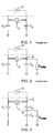
- Figure 1 shows a diagram of a prior art solution for generating an oscillating signal;
- Figure 2 shows a diagram of a second prior art solution for generating an oscillating signal;
- Figure 3 shows a diagram of a third solution for generating an oscillating signal;
- Figure 4 shows an embodiment of the solution according to Figure 3 in more detail;
- Figure 5 shows a diagram of a fourth solution for generating an oscillating signal; and
- Figure 6 shows a diagram of a fifth solution for generating an oscillating signal.
-
- Figure 1 shows a crystal 1. At the resonance frequency, the electric equivalent circuit of the crystal is inductance. Capacitors C1 and C2 are connected to the terminals of the crystal 1. When the capacitance of the capacitors C1 and C2 is selected to be correct, the crystal 1 sees the correct capacitance load at its terminals and begins to oscillate at a desired resonance frequency. In parallel with the crystal 1, a
circuit 2 is connected, shown simplified and with a broken line in Figure 1. Thecircuit 2 is preferably an integrated resonance circuit. Thus, thecircuit 2 forms an oscillator together with the crystal 1 in such a way that the crystal 1 and the capacitors C1 and C2 connected to its terminals are left outside the integrated circuit. - In terms of typical numerical values, it can be presented that it is desirable that the crystal 1 oscillate at a frequency of 12 MHz, and that in such a case the crystal 1 wishes to see a capacitive load of 10 pF at its terminals. To fulfil this requirement, the magnitudes of the capacitors C1 and C2 are selected in such a way, for example, that both C1 and C2 have a magnitude of 20 pF. The order of magnitude of the resistance between the crystal terminal and the ground is in this case so small that it can be left unobserved.
- Figure 2 shows a solution where it is attempted to generate an oscillating signal also for a second circuit with the crystal 1. The oscillating signal can be obtained from a
crystal terminal 3. A buffer is connected to thecrystal terminal 3 for propagating the oscillating signal to the second circuit. For the sake of clarity, Figure 2 shows neither the structure of the buffer in more detail nor the circuit to which the oscillating signal is propagated with the buffer, but the buffer and the second circuit are simply indicated by impedance Rbuffer caused by the buffer. - In the case of Figure 2, capacitance C3s between the
crystal terminal 3 and the ground can be calculated with formula 1, and resistance R3s between thecrystal terminal 3 and the ground can be calculated withformula 2.
f = frequency. -
Formulae 1 and 2 are thus used to convert the connection in parallel of the capacitor C2 and the resistance Rbuffer, shown in Figure 2, with conversion formulae into equivalent connection in series. C3s and R3s thus express, as seen from the crystal terminal, the capacitor and the resistance connected in series in such a way that the connection in series is equivalent to real connection. - If the value of the capacitor C2 is 20 pF, the impedance Rbuffer caused by the buffer is 25 kΩ and the frequency f = 12MHz, then the capacitance C3s between the
crystal terminal 3 and the ground = 20.6 pF. The resistance R3s between thecrystal terminal 3 and the ground is, in turn, 676 Ω. Against the ground the crystal 1 thus sees, instead of an ideal capacitor of 20 pF, a capacitor of 20.6 pF in series with a resistance of 676 Ω. The capacitance C1 seen by the crystal 1 can, in turn, be calculated by means offormula 3. - Thus, in the case of Figure 2, the capacitive load seen by the crystal 1 is C1 = 10,15 pF. This causes the vibration frequency of the crystal 1 to change from what it is in the case of Figure 1. Converting the frequency of the crystal 1 may be excessive, due to which the devices utilizing the oscillating signal do not function in a desired manner. On the other hand, the resistive load of the buffer causes noise and reduces the amplitude of the oscillation. In the worst case, it may be the case that the crystal 1 does not begin to oscillate at all.
- Figure 3 shows a solution deviating from the solution of Figure 2 in such a way that the capacitor C2 of Figure 2 has been replaced by two capacitors C3 and C4 connected in series. Thus, in this case, the capacitor C2 of 20 pF, for example, is replaced by two capacitors C3 and C4 connected in series, the magnitude of each being 40 pF, in other words 2 C2 = C3 = C4. Thus, a capacitive voltage divider is formed at the
terminal 3 of the crystal by means of two capacitors. The buffer is connected to the voltage divider atpoint 4 between the capacitors C3 and C4. - If the values of different components are of a corresponding type also in the solution of Figure 3, i.e., if, for example, the impedance Rbuffer caused by the buffer is 25 kΩ, the capacitance C4s between
point 4 and the ground can be calculated in accordance withformule 4.
- In this case, therefore, the capacitance C4s between
point 4 and the ground = 40,3 pF. The total capacitance C3s between the terminal 3 and the ground is, in turn, 20.07 pF. The capacitive load seen by thecrystal 3 is, in turn, 10.02 pF. Thus, the capacitive load seen by the crystal 1 is thus nearly equal to the capacitive load seen by the crystal 1 in the case of Figure 1. Therefore, in the case of Figure 3 the frequency of the crystal 1 does not change essentially, although in addition to thecircuit 2, also a buffer is connected to the crystal 1. - The resistance R4s between
point 4 and the ground can be calculated by means offormula 5.
- As with
formulae 1 and 2, the conversion into equivalent connection in series is thus calculated by means offormulae - Thus, R4s = 172 Ω. The total resistance R3s between the
terminal 3 of the crystal and the ground is of the same order of magnitude, because the capacitor C3 has little effect on the magnitude of the resistance. Thus, the load caused by the buffer, affecting the amplitude of the oscillation, is in the case of Figure 3 significantly smaller than in Figure 2. - In the above-mentioned example, it is assumed that the buffer causes a fully resistive load. Depending on the buffer topology, the load caused by it may naturally also be capacitive. Depending on the impedance caused by the buffer, however, it is possible in all cases to calculate the change in the impedance, seen by the crystal terminals, by applying the above-described principles. However, it can be seen from the solution of Figure 3 that the effect of the buffer impedance on the impedance seen by the crystal terminals is not at all as great as in the case of Figure 2. The impedance state of an active buffer may vary. When dead, for example, the buffer impedance may be different than when active. However, as noted, this change in the impedance does not significantly affect the impedance seen by the crystal terminals.
- Capacitances C3 and C4 do not necessarily have to be equal. By the mutual magnitudes of the capacitances C3 and C4 it is possible to control how much the buffer impedance is to affect the impedance seen by the crystal terminals. If the value of the capacitor C4 is changed to be higher and the value of the capacitor C3 is changed to be lower, the oscillation amplitude to the buffer is reduced, but the crystal 1 sees a smaller change in the capacitance. If, on the other hand, the amplitude of the oscillation to be fed to the buffer must be relatively high, the value of the capacitor C3 is selected to be higher and the value of the capacitor C4 to be lower if this will not be too detrimental because of the change in the crystal frequency. Thus, also the crystal frequency can be controlled in a desired manner by means of the capacitors C3 and C4.
- Owing to the capacitive voltage divider, the voltage at
point 4 may vary without being detrimental to the crystal 1. Thus, biasing the buffer voltage can be performed in a desired manner, which is not possible in the case of the embodiment of Figure 2. - The solution of Figure 4 corresponds to that of Figure 3, but Figure 4 shows the
buffer 5 in more detail. For illustrative purposes, thebuffer 5 in Figure 4 is surrounded by a broken line. As regards the topology, thebuffer 5 may be an MOS inverter shown in Figure 4, or any other buffer known per se. It depends on the topology of thebuffer 5 how it affects the impedance seen by the crystal terminals. For instance, an MOS buffer would increase the capacitive load, whereas the bipolar stage would also increase the resistive load. - Figure 4 further shows an outlet pin 6, from which the reference frequency can be supplied to another
integrated circuit 7, for example. - Figure 5 shows an embodiment where a voltage divider is formed at the
first terminal 3 of the crystal 1 in a way corresponding to the embodiment of Figure 3. In the embodiment of Figure 5, also thesecond terminal 8 of the crystal is provided with a capacitive voltage divider in a corresponding manner. With the solution of Figure 5, the oscillating frequency can be fed to three different circuits. Naturally, a prerequisite for this is that the crystal 1 fulfils the requirements of all of the three different circuits. Capacitors C5 and C6 may be equal to the capacitors C3 and C4, but their values may naturally also be different. Likewise, the buffers may be similar or different, whereby also the impedances Rbuffer1 and Rbuffer2 are correspondingly either similar or different. - Figure 6 shows a solution where the voltage division of the
first terminal 3 of the crystal is provided by using three capacitors C7, C8 and C9. This solution allows two buffers Rbuffer1 and Rbuffer2 to be arranged in connection with thefirst terminal 3 of the crystal. In connection with thesecond terminal 8 of the crystal, there is voltage division similar to that in Figure 5, whereby one buffer Rbuffer2 is arranged in connection with thesecond terminal 8 of the crystal. Thus, in the case of Figure 6, the oscillating signal can be supplied to four different circuits. If the requirements of the circuits are suitable for the signal and if the impedance change caused by the circuit buffers, as seen from the terminals of the crystal 1, is not too great, a solution of this type allows the oscillating signal to be supplied to even four or more circuits. - The solutions presented are particularly suitable for use with mobile phones or other mobile stations.
- The drawings and the related description are only intended to illustrate the idea of the invention. The details of the invention may vary within the scope of the claims. Thus, the capacitive voltage division may be carried out in ways other than those shown in the figures.
Claims (11)
- A method for arranging a crystal to generate an oscillating signal for a circuit, in which method the crystal (1) is loaded with capacitance in such a way that the crystal (1) begins to oscillate at a desired frequency with a resonance circuit (2), characterized by carrying out capacitive voltage division to at least one terminal (3) of the crystal (1) with a voltage divider, and supplying the oscillating signal of the crystal (1) from the voltage divider to a second circuit (7).
- A method according to claim 1, characterized by carrying out capacitive voltage division to both terminals (3, 8) of the crystal.
- A method according to claim 1 or 2, characterized by supplying the oscillating signal of the crystal (1) from the voltage divider to several circuits.
- An oscillating circuit comprising a crystal (1), and capacitors (C1 - C9) that load the crystal (1) in such a way that the crystal (1) oscillates at a desired frequency with a resonance circuit (2) connected to the crystal (1), characterized in that at least two capacitors (C3, C4) are connected in series at at least one terminal (3) of the crystal (1) in such a way that the capacitors (C3, C4) form a capacitive voltage divider and that a buffer (5) is connected between the capacitors (C3, C4) for supplying the oscillating signal of the crystal (1) to a second circuit (7).
- An oscillating circuit according to claim 4, characterized in that at least two capacitors (C3 - C9) are connected in series at both terminals (3, 8) of the crystal to form a capacitive voltage divider, and a buffer (5) is connected between the capacitors in such a way that the crystal (1) is arranged to supply the oscillating signal to at least three circuits.
- An oscillating circuit according to claim 4 or 5, characterized in that at least three capacitors are connected in series at at least one terminal of the crystal, whereby an oscillating signal of the crystal is suppliable from at least one terminal (3, 8) of the crystal to at least two different circuits.
- An oscillating circuit according to claim 4 or 5, characterized in that at least two capacitors (C3 - C6) of substantially equal magnitude are connected to at least one terminal (3, 8) of the crystal.
- A mobile station comprising an oscillating circuit that is arranged to generate an oscillating signal required by the mobile station, whereby the oscillating circuit comprises a crystal (1), and capacitors (C1 - C9) that load the crystal (1) in such a way that the crystal (1) oscillates at a desired frequency with a resonance circuit (2) connected to the crystal (1), characterized in that at least two capacitors (C3, C4) are connected in series at at least one terminal (3) of the crystal (1) in such a way that the capacitors (C3, C4) form a capacitive voltage divider and that a buffer (5) is connected between the capacitors (C3, C4) for supplying the oscillating signal of the crystal (1) to a second circuit (7).
- A mobile station according to claim 8, characterized in that at least two capacitors (C3 - C9) are connected in series at both terminals (3, 8) of the crystal to form a capacitive voltage divider, and a buffer (5) is connected between the capacitors in such a way that the crystal (1) is arranged to supply the oscillating signal to at least three circuits.
- A mobile station according to claim 8 or 9, characterized in that at least three capacitors are connected in series at at least one terminal of the crystal, whereby the oscillating signal of the crystal is suppliable from one terminal (3, 8) of the crystal to at least two different circuits.
- A mobile station according to claim 8 or 9, characterized in that at least two capacitors (C3 - C6) of substantially equal magnitude are connected to at least one terminal (3, 8) of the crystal.
Applications Claiming Priority (2)
| Application Number | Priority Date | Filing Date | Title |
|---|---|---|---|
| FI20045198A FI116760B (en) | 2004-05-31 | 2004-05-31 | Apparatus of crystal for generating vibration signal |
| FI20045198 | 2004-05-31 |
Publications (1)
| Publication Number | Publication Date |
|---|---|
| EP1603227A1 true EP1603227A1 (en) | 2005-12-07 |
Family
ID=32338474
Family Applications (1)
| Application Number | Title | Priority Date | Filing Date |
|---|---|---|---|
| EP05104388A Withdrawn EP1603227A1 (en) | 2004-05-31 | 2005-05-24 | Arranging a crystal to generate an oscillating signal |
Country Status (3)
| Country | Link |
|---|---|
| US (1) | US7271671B2 (en) |
| EP (1) | EP1603227A1 (en) |
| FI (1) | FI116760B (en) |
Families Citing this family (2)
| Publication number | Priority date | Publication date | Assignee | Title |
|---|---|---|---|---|
| US9869698B2 (en) * | 2010-02-11 | 2018-01-16 | Landis+Gyr Llc | Oscillator circuit with RF suppression |
| US10574181B2 (en) * | 2018-05-17 | 2020-02-25 | Microsoft Technology Licensing, Llc | Circuit with shunt path |
Family Cites Families (8)
| Publication number | Priority date | Publication date | Assignee | Title |
|---|---|---|---|---|
| NL7001606A (en) * | 1970-02-05 | 1971-08-09 | ||
| CH450474A4 (en) | 1974-04-01 | 1976-02-27 | ||
| DE3022836C1 (en) * | 1980-06-19 | 1981-10-29 | Papst-Motoren Kg, 7742 St Georgen | Brushless DC motor |
| US6191661B1 (en) | 1997-10-30 | 2001-02-20 | Nippon Precision Circuits, Inc. | Oscillator circuit with reduced capacity for AC coupling capacitor |
| FI20002168A7 (en) * | 1999-10-12 | 2001-04-13 | Toyo Communication Equipment Co Ltd | Piezoelectric oscillator |
| US6507248B2 (en) | 2000-05-29 | 2003-01-14 | Citizen Watch Co., Ltd. | Voltage-controlled crystal oscillator |
| JP3923285B2 (en) | 2001-07-24 | 2007-05-30 | 日本電波工業株式会社 | Crystal oscillator |
| US6771136B1 (en) * | 2001-12-10 | 2004-08-03 | Cypress Semiconductor Corp. | System and method for restoring the mark and space ratio of a clocking signal output from an oscillator |
-
2004
- 2004-05-31 FI FI20045198A patent/FI116760B/en not_active IP Right Cessation
-
2005
- 2005-05-24 EP EP05104388A patent/EP1603227A1/en not_active Withdrawn
- 2005-05-27 US US11/140,505 patent/US7271671B2/en not_active Expired - Lifetime
Non-Patent Citations (1)
| Title |
|---|
| ECCLES M: "APPLYING CRYSTALS", ELECTRONICS WORLD (INCL. WIRELESS WORLD), REED BUSINESS PUBLISHING, SUTTON, SURREY, GB, vol. 100, no. 1701, 1 August 1994 (1994-08-01), pages 659 - 663, XP000460680, ISSN: 0959-8332 * |
Also Published As
| Publication number | Publication date |
|---|---|
| FI20045198A0 (en) | 2004-05-31 |
| US20050270112A1 (en) | 2005-12-08 |
| US7271671B2 (en) | 2007-09-18 |
| FI20045198L (en) | 2005-12-01 |
| FI116760B (en) | 2006-02-15 |
Similar Documents
| Publication | Publication Date | Title |
|---|---|---|
| US7012476B2 (en) | Voltage-controlled oscillator, clock converter, and electronic device | |
| CN103166573B (en) | Voltage controlled oscillator | |
| JP2003347936A (en) | Clock shaping circuit and electronic equipment | |
| US7157980B2 (en) | Clock converter and electronic apparatus with the same | |
| US9899991B2 (en) | Circuits and methods of synchronizing differential ring-type oscillators | |
| US8044730B2 (en) | Secondary vibration damping type crystal oscillator circuit | |
| CN104115425A (en) | Technique for crosstalk reduction | |
| US20090295491A1 (en) | Carrier Generator | |
| JP4228660B2 (en) | Voltage controlled oscillator and electronic equipment using the same | |
| KR102191295B1 (en) | Notch Filtering Embedded Frequency Tripler | |
| CN100361385C (en) | oscillator | |
| US9866173B2 (en) | Coupling structure for inductive device | |
| EP1603227A1 (en) | Arranging a crystal to generate an oscillating signal | |
| CN100477485C (en) | Arrangement for low power clock generation | |
| US20050275480A1 (en) | Frequency selective oscillator, electronic instrument implementing the same, and method of adjusting frequency control characteristics | |
| JP2004120353A (en) | Voltage-controlled oscillator, clock converter using the voltage-controlled oscillator, and electronic equipment using the clock converter | |
| JP4699402B2 (en) | Oscillator and frequency synthesizer | |
| JP2004120352A (en) | Clock conversion circuit and electronic equipment using the same | |
| KR100538614B1 (en) | Voltage control oscillator | |
| US7119627B2 (en) | Phase-locked loop circuit as well as a voltage-controlled oscillator as used in a phase-locked loop circuit | |
| JP2005026828A (en) | Oscillator and electronic equipment using it | |
| JP2004096449A (en) | Oscillator circuit and electronic equipment using it | |
| JP4228302B2 (en) | Voltage controlled oscillator | |
| JP4399782B2 (en) | Frequency selective oscillator and electronic device equipped with the same | |
| JPH1197627A (en) | Semiconductor integrated circuit and electronic device using the same |
Legal Events
| Date | Code | Title | Description |
|---|---|---|---|
| PUAI | Public reference made under article 153(3) epc to a published international application that has entered the european phase |
Free format text: ORIGINAL CODE: 0009012 |
|
| AK | Designated contracting states |
Kind code of ref document: A1 Designated state(s): AT BE BG CH CY CZ DE DK EE ES FI FR GB GR HU IE IS IT LI LT LU MC NL PL PT RO SE SI SK TR |
|
| AX | Request for extension of the european patent |
Extension state: AL BA HR LV MK YU |
|
| 17P | Request for examination filed |
Effective date: 20060531 |
|
| AKX | Designation fees paid |
Designated state(s): AT BE BG CH CY CZ DE DK EE ES FI FR GB GR HU IE IS IT LI LT LU MC NL PL PT RO SE SI SK TR |
|
| 17Q | First examination report despatched |
Effective date: 20060718 |
|
| GRAP | Despatch of communication of intention to grant a patent |
Free format text: ORIGINAL CODE: EPIDOSNIGR1 |
|
| STAA | Information on the status of an ep patent application or granted ep patent |
Free format text: STATUS: THE APPLICATION IS DEEMED TO BE WITHDRAWN |
|
| 18D | Application deemed to be withdrawn |
Effective date: 20111206 |