EP1603155A1 - Semiconductor device and radiation detector employing it - Google Patents
Semiconductor device and radiation detector employing it Download PDFInfo
- Publication number
- EP1603155A1 EP1603155A1 EP04714016A EP04714016A EP1603155A1 EP 1603155 A1 EP1603155 A1 EP 1603155A1 EP 04714016 A EP04714016 A EP 04714016A EP 04714016 A EP04714016 A EP 04714016A EP 1603155 A1 EP1603155 A1 EP 1603155A1
- Authority
- EP
- European Patent Office
- Prior art keywords
- wiring substrate
- glass
- semiconductor device
- radiation
- hole
- Prior art date
- Legal status (The legal status is an assumption and is not a legal conclusion. Google has not performed a legal analysis and makes no representation as to the accuracy of the status listed.)
- Ceased
Links
Images






Classifications
-
- H—ELECTRICITY
- H05—ELECTRIC TECHNIQUES NOT OTHERWISE PROVIDED FOR
- H05K—PRINTED CIRCUITS; CASINGS OR CONSTRUCTIONAL DETAILS OF ELECTRIC APPARATUS; MANUFACTURE OF ASSEMBLAGES OF ELECTRICAL COMPONENTS
- H05K3/00—Apparatus or processes for manufacturing printed circuits
- H05K3/30—Assembling printed circuits with electric components, e.g. with resistors
- H05K3/32—Assembling printed circuits with electric components, e.g. with resistors electrically connecting electric components or wires to printed circuits
- H05K3/34—Assembling printed circuits with electric components, e.g. with resistors electrically connecting electric components or wires to printed circuits by soldering
- H05K3/341—Surface mounted components
- H05K3/3431—Leadless components
- H05K3/3436—Leadless components having an array of bottom contacts, e.g. pad grid array or ball grid array components
-
- G—PHYSICS
- G01—MEASURING; TESTING
- G01T—MEASUREMENT OF NUCLEAR OR X-RADIATION
- G01T1/00—Measuring X-radiation, gamma radiation, corpuscular radiation, or cosmic radiation
- G01T1/16—Measuring radiation intensity
- G01T1/20—Measuring radiation intensity with scintillation detectors
- G01T1/2018—Scintillation-photodiode combinations
- G01T1/20185—Coupling means between the photodiode and the scintillator, e.g. optical couplings using adhesives with wavelength-shifting fibres
-
- G—PHYSICS
- G01—MEASURING; TESTING
- G01T—MEASUREMENT OF NUCLEAR OR X-RADIATION
- G01T1/00—Measuring X-radiation, gamma radiation, corpuscular radiation, or cosmic radiation
- G01T1/16—Measuring radiation intensity
- G01T1/20—Measuring radiation intensity with scintillation detectors
- G01T1/2018—Scintillation-photodiode combinations
- G01T1/20188—Auxiliary details, e.g. casings or cooling
- G01T1/2019—Shielding against direct hits
-
- H—ELECTRICITY
- H10—SEMICONDUCTOR DEVICES; ELECTRIC SOLID-STATE DEVICES NOT OTHERWISE PROVIDED FOR
- H10F—INORGANIC SEMICONDUCTOR DEVICES SENSITIVE TO INFRARED RADIATION, LIGHT, ELECTROMAGNETIC RADIATION OF SHORTER WAVELENGTH OR CORPUSCULAR RADIATION
- H10F39/00—Integrated devices, or assemblies of multiple devices, comprising at least one element covered by group H10F30/00, e.g. radiation detectors comprising photodiode arrays
- H10F39/10—Integrated devices
- H10F39/12—Image sensors
- H10F39/18—Complementary metal-oxide-semiconductor [CMOS] image sensors; Photodiode array image sensors
- H10F39/189—X-ray, gamma-ray or corpuscular radiation imagers
- H10F39/1898—Indirect radiation image sensors, e.g. using luminescent members
-
- H—ELECTRICITY
- H10—SEMICONDUCTOR DEVICES; ELECTRIC SOLID-STATE DEVICES NOT OTHERWISE PROVIDED FOR
- H10F—INORGANIC SEMICONDUCTOR DEVICES SENSITIVE TO INFRARED RADIATION, LIGHT, ELECTROMAGNETIC RADIATION OF SHORTER WAVELENGTH OR CORPUSCULAR RADIATION
- H10F39/00—Integrated devices, or assemblies of multiple devices, comprising at least one element covered by group H10F30/00, e.g. radiation detectors comprising photodiode arrays
- H10F39/80—Constructional details of image sensors
- H10F39/804—Containers or encapsulations
-
- H—ELECTRICITY
- H10—SEMICONDUCTOR DEVICES; ELECTRIC SOLID-STATE DEVICES NOT OTHERWISE PROVIDED FOR
- H10F—INORGANIC SEMICONDUCTOR DEVICES SENSITIVE TO INFRARED RADIATION, LIGHT, ELECTROMAGNETIC RADIATION OF SHORTER WAVELENGTH OR CORPUSCULAR RADIATION
- H10F39/00—Integrated devices, or assemblies of multiple devices, comprising at least one element covered by group H10F30/00, e.g. radiation detectors comprising photodiode arrays
- H10F39/80—Constructional details of image sensors
- H10F39/809—Constructional details of image sensors of hybrid image sensors
-
- H—ELECTRICITY
- H10—SEMICONDUCTOR DEVICES; ELECTRIC SOLID-STATE DEVICES NOT OTHERWISE PROVIDED FOR
- H10W—GENERIC PACKAGES, INTERCONNECTIONS, CONNECTORS OR OTHER CONSTRUCTIONAL DETAILS OF DEVICES COVERED BY CLASS H10
- H10W70/00—Package substrates; Interposers; Redistribution layers [RDL]
- H10W70/60—Insulating or insulated package substrates; Interposers; Redistribution layers
- H10W70/67—Insulating or insulated package substrates; Interposers; Redistribution layers characterised by their insulating layers or insulating parts
- H10W70/68—Shapes or dispositions thereof
-
- H—ELECTRICITY
- H05—ELECTRIC TECHNIQUES NOT OTHERWISE PROVIDED FOR
- H05K—PRINTED CIRCUITS; CASINGS OR CONSTRUCTIONAL DETAILS OF ELECTRIC APPARATUS; MANUFACTURE OF ASSEMBLAGES OF ELECTRICAL COMPONENTS
- H05K1/00—Printed circuits
- H05K1/02—Details
- H05K1/03—Use of materials for the substrate
- H05K1/0306—Inorganic insulating substrates, e.g. ceramic, glass
-
- H—ELECTRICITY
- H05—ELECTRIC TECHNIQUES NOT OTHERWISE PROVIDED FOR
- H05K—PRINTED CIRCUITS; CASINGS OR CONSTRUCTIONAL DETAILS OF ELECTRIC APPARATUS; MANUFACTURE OF ASSEMBLAGES OF ELECTRICAL COMPONENTS
- H05K2201/00—Indexing scheme relating to printed circuits covered by H05K1/00
- H05K2201/09—Shape and layout
- H05K2201/09818—Shape or layout details not covered by a single group of H05K2201/09009 - H05K2201/09809
- H05K2201/09827—Tapered, e.g. tapered hole, via or groove
-
- H—ELECTRICITY
- H05—ELECTRIC TECHNIQUES NOT OTHERWISE PROVIDED FOR
- H05K—PRINTED CIRCUITS; CASINGS OR CONSTRUCTIONAL DETAILS OF ELECTRIC APPARATUS; MANUFACTURE OF ASSEMBLAGES OF ELECTRICAL COMPONENTS
- H05K2203/00—Indexing scheme relating to apparatus or processes for manufacturing printed circuits covered by H05K3/00
- H05K2203/04—Soldering or other types of metallurgic bonding
- H05K2203/0455—PTH for surface mount device [SMD], e.g. wherein solder flows through the PTH during mounting
-
- H—ELECTRICITY
- H10—SEMICONDUCTOR DEVICES; ELECTRIC SOLID-STATE DEVICES NOT OTHERWISE PROVIDED FOR
- H10W—GENERIC PACKAGES, INTERCONNECTIONS, CONNECTORS OR OTHER CONSTRUCTIONAL DETAILS OF DEVICES COVERED BY CLASS H10
- H10W70/00—Package substrates; Interposers; Redistribution layers [RDL]
- H10W70/60—Insulating or insulated package substrates; Interposers; Redistribution layers
- H10W70/67—Insulating or insulated package substrates; Interposers; Redistribution layers characterised by their insulating layers or insulating parts
- H10W70/68—Shapes or dispositions thereof
- H10W70/682—Shapes or dispositions thereof comprising holes having chips therein
-
- H—ELECTRICITY
- H10—SEMICONDUCTOR DEVICES; ELECTRIC SOLID-STATE DEVICES NOT OTHERWISE PROVIDED FOR
- H10W—GENERIC PACKAGES, INTERCONNECTIONS, CONNECTORS OR OTHER CONSTRUCTIONAL DETAILS OF DEVICES COVERED BY CLASS H10
- H10W72/00—Interconnections or connectors in packages
- H10W72/20—Bump connectors, e.g. solder bumps or copper pillars; Dummy bumps; Thermal bumps
- H10W72/221—Structures or relative sizes
- H10W72/227—Multiple bumps having different sizes
-
- H—ELECTRICITY
- H10—SEMICONDUCTOR DEVICES; ELECTRIC SOLID-STATE DEVICES NOT OTHERWISE PROVIDED FOR
- H10W—GENERIC PACKAGES, INTERCONNECTIONS, CONNECTORS OR OTHER CONSTRUCTIONAL DETAILS OF DEVICES COVERED BY CLASS H10
- H10W90/00—Package configurations
- H10W90/701—Package configurations characterised by the relative positions of pads or connectors relative to package parts
- H10W90/721—Package configurations characterised by the relative positions of pads or connectors relative to package parts of bump connectors
- H10W90/724—Package configurations characterised by the relative positions of pads or connectors relative to package parts of bump connectors between a chip and a stacked insulating package substrate, interposer or RDL
-
- Y—GENERAL TAGGING OF NEW TECHNOLOGICAL DEVELOPMENTS; GENERAL TAGGING OF CROSS-SECTIONAL TECHNOLOGIES SPANNING OVER SEVERAL SECTIONS OF THE IPC; TECHNICAL SUBJECTS COVERED BY FORMER USPC CROSS-REFERENCE ART COLLECTIONS [XRACs] AND DIGESTS
- Y02—TECHNOLOGIES OR APPLICATIONS FOR MITIGATION OR ADAPTATION AGAINST CLIMATE CHANGE
- Y02P—CLIMATE CHANGE MITIGATION TECHNOLOGIES IN THE PRODUCTION OR PROCESSING OF GOODS
- Y02P70/00—Climate change mitigation technologies in the production process for final industrial or consumer products
- Y02P70/50—Manufacturing or production processes characterised by the final manufactured product
Definitions
- This invention concerns a semiconductor device, provided with a wiring substrate that is provided with a conduction path that guides an electrical signal, and a radiation detector using this semiconductor device.
- a radiation detector for use in a CT sensor, etc. there is a detector of an arrangement wherein a scintillator is disposed on a light-incident surface of a semiconductor photodetecting element, which is a semiconductor element.
- a radiation detector when an X-ray, ⁇ -ray, charged particle beam or other radiation to be detected is made incident on the scintillator, scintillation light is generated inside the scintillator by the radiation.
- the semiconductor photodetecting element detects the scintillation light that is made incident from the scintillator and output an electrical signal that is in accordance with the intensity of the radiation.
- a signal processing element is provided.
- an arrangement for electrically connecting the semiconductor element with the signal processing element and transmitting the electrical signal an arrangement is used wherein a semiconductor device is arranged in one united body by connecting the semiconductor element to a wiring substrate that is provided with a conduction path and the signal processing element is connected to the wiring substrate of this semiconductor device.
- a semiconductor device using a wiring substrate is used in various applications besides radiation detectors (see for example, Japanese Patent No. 2555720 and Japanese Patent Application Laid-Open No. H3-203341).
- the semiconductor element and the corresponding conduction path of the wiring substrate are electrically connected via a bump electrode provided on the semiconductor element.
- This invention has been made to resolve the above issue and an object thereof is to provide a semiconductor device, with which the semiconductor element and the corresponding conduction path of the wiring substrate are connected satisfactorily, and a radiation detector using such a semiconductor device.
- this invention provides a semiconductor device comprising: (1) a semiconductor element, outputting an electrical signal; and (2) a wiring substrate, provided with a conduction path, guiding the electrical signal between a signal input surface and a signal output surface, and connected to the semiconductor element at the signal input surface; and wherein (3) the wiring substrate comprises: a glass substrate, provided with a through hole, with which the opening area at the signal input surface is larger than the opening area at a predetermined position in the interior of the glass substrate; and a conductive member, disposed in the through hole and functioning as the conduction path by providing electrical continuity between the signal input surface and the signal output surface; and (4) the semiconductor element and the conductive member of the wiring substrate are electrically connected via a bump electrode formed in correspondence with the conductive member.
- a glass substrate having a conductive member, serving as a conduction path, provided at a through hole that is formed to a predetermined shape and extending from the input surface to the output surface, is used as the wiring substrate that connects the semiconductor photodetecting element or other semiconductor element.
- the bump electrode of the semiconductor element is made to correspond to the through hole and conductive member to connect the semiconductor element with the corresponding conductive member of the wiring substrate.
- the conductive member is preferably formed on the inner wall of the through hole provided in the glass substrate.
- the glass substrate is preferably arranged by cutting a bundle-form glass member, formed by bundling fiber-form glass members, each comprising a core glass portion and a coating glass portion, provided at the periphery of the core glass portion, to a desired thickness and has the through hole formed therein by removal of the core glass portion.
- the wiring substrate can thus be arranged by the glass substrate with which the through holes for disposing the conductive members are formed at the desired hole diameter and pitch.
- the through hole in the glass substrate has a predetermined range thereof at the signal input surface side formed to a tapered shape, with which the opening area decreases gradually from the signal input surface towards the interior of the glass substrate.
- the through hole in the glass substrate has a predetermined range thereof at the signal input surface side formed to a recessed shape of a predetermined opening area that is greater than the opening area in a range that includes a predetermined position in the interior of the glass substrate.
- the glass substrate may have an arrangement provided with, as the through hole, at least a first through hole of a predetermined opening area and a second through hole that differs in opening area from the first through hole.
- the opening areas of the through holes can be set favorably in accordance with the size, height, etc., of the bump electrodes that are to be connected to the conductive members provided at the through holes.
- Signal processing means which is connected to the signal output surface of the wiring substrate and processes the electrical signal from the semiconductor element may furthermore be provided.
- a semiconductor device wherein the electrical signal output from the semiconductor element is processed by the signal processing means, is thereby achieved.
- This invention's radiation detector is a radiation detector arranged so as to include the above-described semiconductor device and comprises: (1) radiation detecting means that includes the semiconductor element and outputs the electrical signal upon detection of incident radiation; (2) signal processing means, processing the electrical signal from the radiation detecting means; and (3) a wiring substrate section, including the wiring substrate and having the signal input surface and the signal output surface being connected to the radiation detecting means and the signal processing means, respectively.
- the wiring substrate which comprises the above-described semiconductor device along with the semiconductor element included in the radiation detecting means, is used as the wiring substrate section that electrically connects the radiation detecting means and the signal processing means and transmits the detected signal, which is the electrical signal.
- the glass substrate used in the wiring substrate is preferably formed of a predetermined glass material having a radiation shielding function.
- the transmission of radiation from the radiation detecting means to the signal processing means can thereby be restrained.
- a glass material containing lead can be cited as an example of such a glass material.
- the radiation detecting means can be arranged with a scintillator, which generates scintillation light upon incidence of radiation, and the semiconductor photodetecting element, which detects the scintillation light from the scintillator.
- the semiconductor photodetecting element which detects the incident radiation may be used instead as the radiation detecting means.
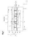
- Fig. 1 is a sectional side view showing the cross-sectional structure of an embodiment of a semiconductor device and a radiation detector using the same.
- Fig. 2 is a perspective view showing the arrangement of the radiation detector of Fig. 1 in an exploded manner.
- Fig. 3A and Fig. 3B are plan views respectively showing the arrangement of (A) a signal input surface and (B) a signal output surface of the wiring substrate.
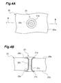
- Fig. 4A and Fig. 4B are diagrams showing an example of the arrangement of a through hole of the wiring substrate and a conductive member disposed in the through hole.
- Fig. 5A and Fig. 5B are diagrams showing an example of the arrangement of through holes and conductive members in a wiring substrate and the connection of these components with bump electrodes.
- Fig. 6A and Fig. 6B are diagrams showing another example of the arrangement of through holes and conductive members in a wiring substrate and the connection of these components with bump electrodes.
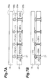
- Fig. 7A and Fig. 7B are diagrams showing another example of the arrangement of through holes and conductive members in a wiring substrate and the connection of these components with bump electrodes.
- Fig. 8A to Fig. 8E are diagrams showing an example of a method of manufacturing a wiring substrate.
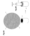
- Fig. 9A and Fig. 9B are diagrams showing an example of a method of manufacturing a wiring substrate.
- Fig. 10A and Fig. 10B are diagrams showing an example of a method of manufacturing a wiring substrate.
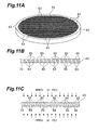
- Fig. 11A to Fig. 11C are diagrams showing an example of a method of manufacturing a wiring substrate.
- Fig. 1 is a sectional side view showing the cross-sectional structure of an embodiment of this invention's semiconductor device and radiation detector.
- Fig. 2 is a perspective view showing the arrangement of the semiconductor device and the radiation detector shown in Fig. 1 with the respective components being shown in exploded manner.
- an axis along the direction of incidence of radiation shall be taken as the z-axis and two axes orthogonal to the z-axis shall be taken as the x-axis and the y-axis in the drawings that follows.
- the negative direction of the z-axis is the conduction direction from a signal input surface to a signal output surface of a wiring substrate and is the alignment direction of the respective components of the radiation detector.
- the radiation detector shown in Fig. 1 is provided with a scintillator 10, a semiconductor device 5, and a signal processing section 3. As shown in Fig. 2, these are positioned in that order from the upstream side (upper side of the figure) to the downstream side (lower side) along the predetermined alignment direction.
- semiconductor device 5 which comprises a photodiode array 15 and a wiring substrate 20, shall now be described.
- Photodiode array (PD array) 15 comprises an upstream side portion of semiconductor device 5.
- This PD array 15 is a semiconductor photodetecting element array in which a plurality of photodiodes (PDs), which are semiconductor elements that detect incident light and output electrical signals corresponding to the incident light intensity, are arrayed.
- PDs photodiodes
- a lower surface 15b of PD array 15 is a signal output surface for outputting detected signals from the respective photodiodes 16.
- 16 bump electrodes 17, which are detected signal output electrodes are arrayed in a 4 ⁇ 4 manner in correspondence with the respective photodiodes 16.
- bump electrodes that serve as substrate electrodes (common electrodes) take on the same form as the electrodes for the output of the detected signals.
- Wiring substrate 20 comprises a downstream side portion of semiconductor device 5. This wiring substrate 20 is provided with conduction paths that guide electrical signals between a signal input surface 20a and a signal output surface 20b and the above-described PD array 15 is connected to signal input surface 20a.
- a glass substrate arranged by forming a bundle-form glass member by bundling fiber-form glass members (glass fibers), each comprising a core glass portion and a coating glass portion, provided at the periphery of the core glass portion, and cutting the bundle-form glass member to a desired thickness in a predetermined direction that intersects the axes of the glass fibers, is used in wiring substrate 20.
- fiber-form glass members glass fibers
- semiconductor device 5 is applied to a radiation detector, a lead glass material, which contains lead or other predetermined glass material having a radiation shielding function, is used as the glass material of wiring substrate 20.
- Fig. 3A and Fig. 3B are respectively plan views showing the arrangement of wiring substrate 20, with Fig. 3A showing signal input surface 20a, which is the upper surface, and Fig. 3B showing signal output surface 20b, which is the lower surface. Only the principal portions are shown in these figures and illustration of portions corresponding to the substrate electrodes of the PD array, etc., are omitted from illustration.
- Fig. 4A and Fig. 4B are drawings showing an example of the arrangement of a through hole 20c of a wiring substrate 20 and a conductive member 21 provided in through hole 20c, with Fig. 4A being a top view and Fig. 4B being a section taken on arrows I-I.
- each through hole 20c is formed to have a circular cross-sectional shape with an axis perpendicular to input surface 20a and output surface 20b of wiring substrate 20 as its central axis.
- a predetermined range of this through hole 20c at the signal input surface 20a side is formed as a tapered part 20d of tapered shape, with which the opening area decreases successively from input surface 20a towards the interior of the glass substrate.
- a predetermined range at the signal output surface 20b side is formed as a tapered part 20e of tapered shape, with which the opening area decreases successively from output surface 20b towards the interior.
- conductive members 21, each of which provides electrical continuity between input surface 20a and output surface 20b, are provided as members formed on the inner walls of through holes 20c.
- a conducting portion 21c is formed at the inner wall of the interior of each through hole 20c that includes tapered parts 20d and 20e.
- an input portion 21a which is continuous with conducting portion 21c, is formed on input surface 20a at an outer peripheral portion of tapered part 20d.
- an output portion 21b which is continuous with conducting portion 21c, is formed on output surface 20b at an outer peripheral portion of tapered part 20e.
- Each conductive member 21, which is to serve as a conduction path of wiring substrate 20, is arranged by conducting portion 21c, input portion 21a, and output portion 21b.
- input portions 21a of conductive members 21 are disposed on input surface 20a of wiring substrate 20 at positions corresponding to bump electrodes 17 on output surface 15b of PD array 15 .
- bump electrodes 17 of PD array 15 are formed to correspond to through holes 20c and conductive members 21 of wiring substrate 20 and input portions 21a are arranged as electrode pads to which bump electrodes 17 are connected.
- Each bump electrode 17 is connected to the corresponding conductive member 21 of wiring substrate 20 in a manner such that a portion of bump electrode 17 enters into the interior of through hole 20c in which conductive member 21 is disposed.
- Photodiodes 16, which output the detected signals at PD array 15, are thus electrically connected via bump electrodes 17 to conductive members 21, which are the conduction paths of wiring substrate 20 that transmit the detected signals.
- Electrode pads 22 are formed in addition to output portions 21b of conductive members 21 as shown in Fig. 3B. Electrode pads 22 are electrically connected via wirings 23 to output portions 21b of the corresponding conductive members 21. Electrode pads 24 are also formed on output surface 20b. These electrode pads 24 are used for connection with a housing 40 to be described later.
- a scintillator 10 is disposed at the upstream side of PD array 15 of semiconductor device 5, and an upper surface 10a thereof is arranged as a radiation-incident surface of the radiation detector. Upon incidence of an X-ray, ⁇ -ray, charged particle beam or other radiation from incident surface 10a, scintillator 10 generates scintillation light of a predetermined wavelength.
- a light exit surface 10b, which is the lower surface of scintillator 10, and a light-incident surface 15a, which is the upper surface of PD array 15, are optically connected and bonded together via an optical adhesive agent 11 that allows the transmission of the scintillation light.
- a radiation detecting section 1 of the present radiation detector is arranged by scintillator 10 and PD array 15.
- This radiation detecting section 1 is a detecting means that detects radiation made incident thereon and outputs detected signals as electrical signals that correspond to the intensity of the radiation.
- a wiring substrate section 2, which connects radiation detecting section 1 and signal processing section 3, is arranged from wiring substrate 20.
- Signal processing section 3 and housing (package) 40 are disposed at the downstream side of wiring substrate 20 of semiconductor device 5.
- signal processing section 3 comprises a signal processing element 30, provided with a signal processing circuit for processing the detected signals from PD array 15 .
- Bump electrodes 31 are formed on the upper surface of signal processing element 30. These bump electrodes 31 are disposed at positions corresponding to electrode pads 22 on output surface 20b of wiring substrate 20. Conductive members 21, which are the conduction paths of wiring substrate 20 that transmit the detected signals, are thus electrically connected via output portions 21b, wirings 23, electrode pads 22, and bump electrodes 31 to the signal processing circuit provided in signal processing element 30.
- the drive signals of the signal processing circuit and the output signals from the signal processing circuit are likewise connected via bump electrodes to predetermined electrode pads on output surface 20b of wiring substrate 20 and electrically connected to predetermined leads 43 via electrode pads 24 on output surface 20b of wiring substrate 20 and bump electrodes 44 on housing 40.
- Housing 40 is a holding member that integrally holds scintillator 10, semiconductor device 5, which is comprised of PD array 15 and wiring substrate 20, and signal processing element 30.
- This housing 40 has an element housing part 41, which is provided as a recessed part on the upper surface of the housing and houses signal processing element 30 in the interior thereof, and a supporting part 42, which is disposed at the outer periphery of element housing part 41, is connected via bump electrodes 44 to electrode pads 24 of wiring substrate 20, and supports scintillator 10, semiconductor device 5, and signal processing element 30.
- Leads 43 used for input and output of electrical signals with respect to the exterior, are provided on the lower surface of housing 40.
- the electrical signals output from the respective photodiodes 16 of PD array 15 are input, successively via the corresponding bump electrodes 17, conductive members 21 of wiring substrate 20, and bump electrodes 31, into signal processing element 30. Signal processing is then carried out at the signal processing circuit of signal processing element 30.
- a glass substrate having conductive members 21, serving as conductive paths, provided in through holes 20c that extend from input surface 20a to output surface 20b and are formed to shapes having tapered parts 20d and 20e, is used as wiring substrate 20 that connects PD array 15, which is a semiconductor element array.
- Photodiodes 16 of PD array 15, which are the semiconductor elements, and the corresponding conductive members 21 of wiring substrate 20 are connected upon making bump electrodes 17 of PD array 15 correspond to through holes 20c and conductive members 21. Bump electrodes 17 and conductive members 21 can thus be connected satisfactorily.
- wiring substrate 20 which comprises semiconductor device 5 along with PD array 15 that is included in radiation detecting section 1, is used as wiring substrate section 2 that electrically connects radiation detecting section 1 and signal processing section 3 and transmits the detected signal.
- a substrate formed of a predetermined glass material having a radiation shielding function, is preferably used as the glass substrate used in wiring substrate 20.
- the transmission of radiation from radiation detecting section 1, positioned at the upper surface 20a side of wiring substrate 20, to signal processing section 3, positioned at the lower surface 20b side, can thereby be restrained.
- Glass materials containing lead can be cited as examples of such a glass material.
- the amount of lead to be contained in the glass material is preferably set as suited in accordance with the degree of radiation shielding function, etc., that are required of the radiation detector.
- a glass material having a radiation shielding function besides lead glass may be used instead.
- a glass material without a radiation shielding function may be used.
- a glass substrate formed integrally from a plurality of glass fibers and provided at predetermined positions thereof with through holes 20c that are formed by removing the core glass portions, is used as the glass substrate of wiring substrate 20.
- Wiring substrate 20 can thus be arranged by a glass substrate, wherein through holes 20c for disposing conductive members 21 are formed to have the desired hole diameter and pitch.
- through holes 20c can be formed to have a microscopic hole diameter and pitch.
- Wiring substrate 20 can also be readily made large in area and thin. As long as through holes of the above-described shape are provided, a glass substrate of another arrangement may be used instead.
- Fig. 5A and Fig. 5B are diagrams showing an example of a specific arrangement of through holes and conductive members in the wiring substrate and the connection with bump electrodes, with Fig. 5A showing a state prior to connection and Fig. 5B showing a state after connection.
- semiconductor device 5 is arranged using wiring substrate 20, wherein conductive members 21 are disposed in through holes 20c of the glass substrate formed from glass fibers, and PD array 15, having bump electrodes 17 formed in correspondence with through holes 20c and conductive members 21.
- bump electrodes 17 provided on output surface 15b of PD array 15, are illustrated, and of these bump electrodes 17, the two at the inner side are somewhat small bump electrodes 171 and the two at the outer side are bump electrodes 172 that are larger than bump electrodes 171.
- portions of bump electrodes 17 respectively enter into the interiors of through holes 20c, provided with the corresponding conductive members 21, in accordance with the sizes, heights, etc., of the respective bump electrodes 17 as shown in Fig. 5B.
- Bump electrodes 17 are thus prevented from collapsing excessively and spreading to the surroundings of the corresponding electrode pads, etc., in the mounting process.
- the bump electrodes therefore do not become shorted mutually and bump electrodes 17 can thus be connected satisfactorily with the corresponding conductive members 21.
- a predetermined range at the input surface 20a side of each through hole 20c provided in wiring substrate 20 is made a tapered part 20d.
- bump electrode 17 since the opening area (inner diameter of the circular shape) of each through hole 20c becomes larger at the input surface 20a side at which a bump electrode 17 is connected, bump electrode 17 enters into the interior of through hole 20c while being guided by the shape of through hole 20c with tapered part 20d. Bump electrodes 17 can thus be connected securely to conductive members 21.
- such a through hole 20c of wiring substrate 20 is preferably formed so that the opening area at the input surface 20a will be greater than the opening area at a predetermined position (for example, a position within a range that includes the center position and wherein the opening area is fixed) in the interior of the glass substrate.
- a portion of bump electrode 17 is thereby made to enter into the interior of through hole 20c while being guided by the shape of through hole 20c, which becomes large in opening area at the side at which bump electrode 17 is connected, and a semiconductor device and radiation detector can thus be realized with which photodiodes 16 of PD array 15, which are semiconductor elements, are satisfactorily connected via bump electrodes 17 to the corresponding conductive members 21 of wiring substrate 20.
- through hole 20c which becomes large in opening area at the input surface 20a side, is also effective in terms of aspects besides connection with the bump electrode 17.
- the need to make the through holes microscopic in hole diameter arises in cases where the wirings themselves are to be made narrow in pitch, cases where radiation is to be shielded by the glass material of the wiring substrate in a radiation detector, etc.
- each through hole 20c is made to have a tapered shape within a predetermined range at the input surface 20a side
- various other arrangements may be employed as specific arrangements of through holes 20c of a shape, with which the opening area at input surface 20a is larger than the opening area at a predetermined position in the interior of the glass substrate.
- Fig. 6A and Fig. 6B are diagrams showing another example of a specific arrangement of through holes and conductive members in the wiring substrate and the connection with bump electrodes, with Fig. 6A showing a state prior to connection and Fig. 6B showing a state after connection.
- a predetermined range at the input surface 20a side of each through hole 20c provided in wiring substrate 20 is made a recessed part 20f, which is formed to a recessed shape of an opening area (inner diameter of a circular shape) that is larger than the opening area (inner diameter) in a range that includes a predetermined position (for example, the center position) in the interior of the glass substrate.
- a predetermined range at the input surface 20a side is made a tapered part 20d
- bump electrodes 17 can be connected securely to conductive members 21.
- Fig. 7A and Fig. 7B are diagrams showing another example of a specific arrangement of through holes and conductive members in the wiring substrate and the connection with bump electrodes, with Fig. 7A showing a state prior to connection and Fig. 7B showing a state after connection.
- bump electrodes 17, provided on output surface 15b of PD array 15, are illustrated, and as with the example of Fig. 5A, of these bump electrodes 17, the two at the inner side are somewhat small bump electrodes 171 and the two at the outer side are bump electrodes 172 that are larger than bump electrodes 171.
- the two at the inner side that correspond to bump electrodes 171 are arranged as through holes (first through holes) 201c, which are somewhat small in opening area
- the two at the outer side that correspond to bump electrodes 172 are arranged as through holes (second through holes) 202c, which are larger in opening area than through holes 201c.
- the opening areas of the respective through holes 20c can be set favorably in accordance with the sizes, heights, etc., of the bump electrodes 17 to be connected to conductive members 21. Bump electrodes 17 can thereby be connected securely to the corresponding conductive members 21 regardless of differences in their sizes, heights, etc.
- the glass substrate, used in the wiring substrate of the semiconductor device and the radiation detector shown in Fig. 1, and a method of manufacture thereof shall now be described using Fig. 8A to Fig. 11C.
- a general arrangement example of a glass substrate having through holes and a method of manufacture thereof shall be described.
- the glass substrate in the following description differs in shape and arrangement from the wiring substrate used in the radiation detector shown in Fig. 1.
- a base material 61 comprising a core glass portion 63 and a coating glass portion 65, provided at the periphery of core glass portion 63.
- This base material 61 is, for example, approximately 40 to 45mm in outer diameter, with core glass portion 63 being, for example, approximately 28 to 31mm in outer diameter.
- Core glass portion 63 is formed of acid-soluble glass
- coating glass portion 65 is formed of lead glass, soda lime glass, cobal glass, Pyrex glass, etc.
- base material 61 is drawn to prepare a glass fiber 67, which is a glass member of fiber-form.
- the outer diameter of the glass fiber 67 is, for example, approximately 0.4mm.
- a plurality of the above-mentioned glass fibers 67 are bundled and aligned inside a predetermined mold 69.
- a mold 69 having a hexagonal shape as viewed in the direction of the central axes of glass fibers 67, is used and approximately 10,000 glass fibers 67 are loaded inside the mold. Glass fibers 67 are thereby aligned to a hexagonal shape as viewed in the direction of their central axes as shown in Fig. 8D.
- Glass fibers 67 may instead be aligned to take on a triangular or rectangular shape as viewed in the direction of their central axes by using a mold having a triangular or rectangular shape as viewed in the direction of the central axes of glass fibers 67.
- Multi-fiber 71 is, for example, approximately 0.7mm in outer diameter.
- a plurality of the drawn multi-fibers 71 are aligned and fitted inside a predetermined glass tube 73.
- the inner diameter of glass tube 73 is approximately 100mm.
- multi-fibers 71, which have been fitted inside glass tube 73 are fused to each other by heating.
- a glass tube 75 which is narrower than glass tube 73, to one end of glass tube 73 and using a rotary pump, etc., to exhaust air and lower the internal pressure
- multi-fibers 71, which have been fitted inside glass tube 73 can be made to contact each other and glass tube 73 and fused without any gaps upon heating by atmospheric pressure.
- the heating temperature is, for example, approximately 600 degrees, and the internal pressure is approximately 0.5Pa.
- the other end of glass tube 73 is sealed.
- Glass tube 75 and the sealed portion are then removed. Thereafter, a grindstone 79, etc., is used to polish the outer periphery of glass tube 73 and shape of bundle-form glass member 77 is adjusted (outer diameter adjustment) as shown in Fig. 10A.
- a circumferential grinder may be used for this outer diameter adjustment.
- bundle-form glass member 77 is cut to a desired thickness.
- a glass substrate with a shape with which the central axes of the through holes are axes perpendicular to the upper surface and lower surface, is obtained, as the wiring substrate 20 shown in Fig. 1.
- bundle-form glass member 77 may be cut using slicer 81 obliquely at a predetermined angle ⁇ with respect to axis 1, which is perpendicular to the central axis, as shown in Fig. 10B.
- the cut surface of the glass member that has been cut by slicer 81 is then polished.
- a plate-form glass member 83 is formed as shown in Fig. 11A and Fig. 11B.
- a glass member 83 which is obtained by cutting obliquely at the angle ⁇ , is shown as an example.
- core glass portions 63 are removed from plate-like glass member 83 (core removal).
- core glass portions 63 are removed by an etching technique that uses HNO 3 or HCl.
- a plurality of through holes 84, which pass through plate-like glass member 83 in the thickness direction, are thereby formed.
- tapered parts or recessed parts, etc. are formed in the through holes.
- a substrate, with which conductive members that are to serve as conduction paths are formed in the through holes in the glass substrate obtained by the above-described manufacturing method may be used for example. That is, the substrate shape and the number, positions, etc., of the through holes of the glass substrate of this arrangement are set in accordance with the arrangement of the radiation detector. Then by forming the conductive members that are to serve as conduction paths in the through holes provided in the glass substrate and then forming electrical wiring patterns, comprising the necessary electrodes and wirings, on the respective surfaces, a wiring substrate with the arrangement such as that shown in Fig. 3A and Fig. 3B is obtained.
- the glass substrate which is formed by cutting the bundle-form glass member made by bundling the plurality of glass fibers as described above and is provided with through holes by the removal of predetermined core glass portions and the forming of tapered parts, etc., is prepared.
- Wiring substrate 20, used in semiconductor device 5 is then prepared by forming conductive members that are to serve as conduction paths in the through holes and furthermore forming electrical wiring patterns, having the necessary electrodes and wirings, on the respective surfaces that are to become the input surface and the output surface.
- the above-mentioned conductive members and electrical wiring patterns to be formed on the glass substrate may be formed of a conductive metal layer that is formed, for example, of titanium nitride (TiN), nickel (Ni), aluminum (Al), chromium (Cr), copper (Cu), silver (Ag), gold (Au), or an alloy of such metals.
- a metal layer may be a single metal layer, a composite film, or a layered film.
- a metal layer may be formed by vapor deposition, CVD, plating, sputtering, etc., and patterning on the glass substrate may be performed by a photolithography or etching process.
- a method of providing a mask of the desired pattern on the glass substrate, forming a metal layer by an above-mentioned method, and thereafter removing the mask may be employed.
- bump electrodes may furthermore be formed on wiring substrate 20.
- an IC chip of signal processing element 30, having bump electrodes 31 formed thereon is aligned with respect to electrode pads 22 disposed on output surface 20b of wiring substrate 20 and these are then connected physically and electrically.
- PD array 15, having bump electrodes 17 formed thereon is aligned with respect to input portions 21a of conductive members 21, which are disposed on input surface 20a of wiring substrate 20 and function as electrode pads, and these are then connected physically and electrically.
- the bump material for forming bump electrodes 31 and 17 nickel (Ni), copper (Cu), silver (Ag), gold (Au), solder, a resin containing a conductive filler, or a composite material of such materials may for example be used or arranged in a layer structure. Also, an under-bump metal (UBM) may be interposed between the bump electrodes and the electrode pads below.
- UBM under-bump metal
- Housing 40 on which bump electrodes 44 have been formed, is then aligned with respect to electrode pads 24 provided on output surface 20b of wiring substrate 20, and these are connected physically and electrically.
- input/output operations of signals with respect to an external circuit are enabled via leads 43 that are provided at housing 40.
- PD array 15 which is provided as the semiconductor photodetecting element array in semiconductor device 5
- a PD array of a front incident type with which the photodiodes are formed on light-incident surface (front surface) 15a
- a PD array of a back incident type with which the photodiodes are formed on signal output surface (back surface) 15b
- the number, alignment, etc. of the photodiodes that are the photodetecting elements can be set as suited.
- an arrangement of wiring patterns formed on output surface 15b or an arrangement of through electrodes formed in PD array 15, etc. may be employed, according to the specific arrangement of the PD array.
- an arrangement having scintillator 10, which generates scintillation light upon incidence of radiation, and a PD array 15, which is provided with photodiodes 16 that are the semiconductor photodetecting elements that detect the scintillation light from scintillator 10, is employed as the arrangement of radiation detecting section 1.
- Such an arrangement is an indirect detection type arrangement, wherein an incident X-ray or other radiation is converted to light of a predetermined wavelength (for example, visible light) by means of scintillator 10 and then detected by an Si-PD array or other semiconductor photodetecting elements.
- An arrangement which is not provided with a scintillator but is provided with semiconductor detecting elements that detect the incident radiation, may be employed instead as the radiation detecting section.
- Such an arrangement is a direct detection type arrangement, wherein the incident X-ray of other radiation is detected by semiconductor detecting elements formed of CdTe, CdZnTe, etc.
- Such an arrangement can also be realized by making the thickness of Si adequately thick and thereby making it totally depleted and arranging a structure that enables incidence from the rear surface. This corresponds, for example, to an arrangement with which scintillator 10 is removed from the arrangement of Fig. 1 and PD array 15 is replaced by a semiconductor detecting element array.
- the semiconductor device is arranged by the semiconductor detecting element array and the wiring substrate.
- the semiconductor device of the above-described arrangement comprising a semiconductor element and a wiring substrate can be applied to various devices besides a radiation detector.
- elements other than semiconductor photodetecting elements and semiconductor detecting elements may be used as the semiconductor elements.
- the semiconductor device may be arranged by providing, in addition to the wiring substrate and the semiconductor element that is connected to the signal input surface of the wiring substrate, a signal processing element that is connected to the signal output surface of the wiring substrate and thus providing a structure wherein the semiconductor element and the signal processing element, which processes the electrical signal from the semiconductor element, are made integral via the wiring substrate.
- connection of wiring substrate 20 and signal processing element 30, etc. it is preferable to use a direct bonding method of forming electrical connections via bump electrodes as in the above-described embodiment.
- metal bump electrodes as the electrical connection means, the respective components can be electrically connected favorably.
- electrode pads 22 for connection of signal processing element 30 are provided on output surface 20b of wiring substrate 20.
- output portions 21b of conductive members 21 may be used as they are as electrode pads.
- an arrangement wherein filling by an underfill resin after making connections with the bump electrodes, an arrangement employing an anisotropic conductive film (ACF) method, an anisotropic conductive paste (ACP) method, or a non-conductive paste (NCP) method may also be used.
- ACF anisotropic conductive film
- ACP anisotropic conductive paste
- NCP non-conductive paste
- passivation films formed of an insulating substance, may be formed as necessary in the state in which the electrode pads are open.
- this invention's semiconductor device and radiation detector using the same can be used as a semiconductor device and radiation detector using the same, wherein the semiconductor element and the corresponding conduction path of the wiring substrate are connected satisfactorily. That is, with an arrangement, wherein a glass substrate, with which conductive members that are to serve as conduction paths are provided in through holes of shapes that become large in opening area at the input surface, is used as the wiring substrate for connecting semiconductor photodetecting elements and other semiconductor elements and the semiconductor elements and the corresponding conductive members on the wiring substrate are connected upon making the bump electrodes of the semiconductor elements correspond to the through holes and the conductive members, a portion of each bump electrode enters into the interior of a through hole at which a conductive member is provided while being guided by the shape of the through hole that becomes large in opening area at the side at which the bump electrode is connected in the process of mounting the semiconductor elements onto the wiring substrate.
Landscapes
- General Physics & Mathematics (AREA)
- Engineering & Computer Science (AREA)
- Physics & Mathematics (AREA)
- Health & Medical Sciences (AREA)
- Life Sciences & Earth Sciences (AREA)
- Molecular Biology (AREA)
- High Energy & Nuclear Physics (AREA)
- Spectroscopy & Molecular Physics (AREA)
- Microelectronics & Electronic Packaging (AREA)
- Manufacturing & Machinery (AREA)
- Measurement Of Radiation (AREA)
- Solid State Image Pick-Up Elements (AREA)
- Light Receiving Elements (AREA)
- Wire Bonding (AREA)
Abstract
Description
Claims (11)
- A semiconductor device comprising:a semiconductor element, outputting an electrical signal; anda wiring substrate, provided with a conduction path, guiding the electrical signal between a signal input surface and a signal output surface, and connected to the semiconductor element at the signal input surface;the wiring substrate comprising: a glass substrate, provided with a through hole, with which the opening area at the signal input surface is larger than the opening area at a predetermined position in the interior of the glass substrate; and a conductive member, disposed in the through hole and functioning as the conduction path by providing electrical continuity between the signal input surface and the signal output surface; andthe semiconductor element and the conductive member of the wiring substrate being electrically connected via a bump electrode formed in correspondence with the conductive member.
- The semiconductor device according to Claim 1, wherein the conductive member is formed on the inner wall of the through hole provided in the glass substrate.
- The semiconductor device according to Claim 1 or 2, wherein the glass substrate is formed by cutting a bundle-form glass member, formed by bundling fiber-form glass members, each comprising a core glass portion and a coating glass portion, provided at the periphery of the core glass portion, to a desired thickness and has the through hole provided therein by removal of the core glass portion.
- The semiconductor device according to any of Claims 1 through 3, wherein the through hole in the glass substrate has a predetermined range thereof at the signal input surface side formed to a tapered shape, with which the opening area decreases gradually from the signal input surface towards the interior of the glass substrate.
- The semiconductor device according to any of Claims 1 through 3, wherein the through hole in the glass substrate has a predetermined range thereof at the signal input surface side formed to a recessed shape that is of a predetermined opening area that is greater than the opening area in a range that includes a predetermined position in the interior of the glass substrate.
- The semiconductor device according to any of Claims 1 through 5, wherein the glass substrate is provided with, as the through hole, at least a first through hole of a predetermined opening area and a second through hole that differs in opening area from the first through hole.
- The semiconductor device according to any of Claims 1 through 6, further comprising signal processing means, connected to the signal output surface of the wiring substrate and processing the electrical signal from the semiconductor element.
- A radiation detector, arranged so as to include the semiconductor device according to Claim 7 and comprising:radiation detecting means, including the semiconductor element and outputting the electrical signal upon detection of incident radiation;the signal processing means, processing the electrical signal from the radiation detecting means; anda wiring substrate section, including the wiring substrate and having the signal input surface and the signal output surface being connected to the radiation detecting means and the signal processing means, respectively.
- The radiation detector according to Claim 8, wherein the glass substrate is formed of a predetermined glass material having a radiation shielding function.
- The radiation detector according to Claim 8 or 9, wherein the radiation detecting means comprises: a scintillator, generating scintillation light upon incidence of radiation; and the semiconductor element, detecting the scintillation light from the scintillator.
- The radiation detector according to Claim 8 or 9, wherein the radiation detecting means comprises the semiconductor element, detecting incident radiation.
Applications Claiming Priority (3)
| Application Number | Priority Date | Filing Date | Title |
|---|---|---|---|
| JP2003046173A JP4133429B2 (en) | 2003-02-24 | 2003-02-24 | Semiconductor device |
| JP2003046173 | 2003-02-24 | ||
| PCT/JP2004/002136 WO2004075282A1 (en) | 2003-02-24 | 2004-02-24 | Semiconductor device and radiation detector employing it |
Publications (2)
| Publication Number | Publication Date |
|---|---|
| EP1603155A1 true EP1603155A1 (en) | 2005-12-07 |
| EP1603155A4 EP1603155A4 (en) | 2008-08-06 |
Family
ID=32905542
Family Applications (1)
| Application Number | Title | Priority Date | Filing Date |
|---|---|---|---|
| EP04714016A Ceased EP1603155A4 (en) | 2003-02-24 | 2004-02-24 | SEMICONDUCTOR DEVICE AND RADIATION DETECTOR COMPRISING THIS DEVICE |
Country Status (7)
| Country | Link |
|---|---|
| US (1) | US7838994B2 (en) |
| EP (1) | EP1603155A4 (en) |
| JP (1) | JP4133429B2 (en) |
| KR (1) | KR20050105240A (en) |
| CN (1) | CN100407388C (en) |
| TW (1) | TW200428545A (en) |
| WO (1) | WO2004075282A1 (en) |
Cited By (5)
| Publication number | Priority date | Publication date | Assignee | Title |
|---|---|---|---|---|
| EP1653515B1 (en) * | 2004-10-26 | 2008-02-13 | Sony Corporation | Semiconductor image sensor module, method for manufacturing the same as well as camera and method for manufacturing the same |
| EP2041605A4 (en) * | 2006-07-11 | 2012-01-18 | Aeroflex Colorado Springs Inc | TWO-COMPONENT PHOTODIOD DETECTOR |
| EP2367028A3 (en) * | 2010-03-16 | 2013-07-03 | Kabushiki Kaisha Toshiba | Radioactive ray detecting apparatus, method of manufacturing the same, and imaging system |
| EP2103958A3 (en) * | 2004-05-11 | 2013-10-09 | Hamamatsu Photonics K.K. | Radiation imaging device |
| EP2577728A4 (en) * | 2010-06-02 | 2013-11-13 | Sony Corp | SEMICONDUCTOR DEVICE, SEMICONDUCTOR IMAGING DEVICE, AND CAMERA SYSTEM |
Families Citing this family (28)
| Publication number | Priority date | Publication date | Assignee | Title |
|---|---|---|---|---|
| JP4138529B2 (en) * | 2003-02-24 | 2008-08-27 | 浜松ホトニクス株式会社 | Semiconductor device and radiation detector using the same |
| GB2449853B (en) | 2007-06-04 | 2012-02-08 | Detection Technology Oy | Photodetector for imaging system |
| JP4855439B2 (en) * | 2008-04-30 | 2012-01-18 | 浜松ホトニクス株式会社 | Radiation detector |
| DE102010011582B4 (en) * | 2010-03-16 | 2011-12-01 | Siemens Aktiengesellschaft | Detector module for a radiation detector and radiation detector |
| US8824706B2 (en) | 2011-08-30 | 2014-09-02 | Qualcomm Mems Technologies, Inc. | Piezoelectric microphone fabricated on glass |
| US8724832B2 (en) | 2011-08-30 | 2014-05-13 | Qualcomm Mems Technologies, Inc. | Piezoelectric microphone fabricated on glass |
| JP5791461B2 (en) * | 2011-10-21 | 2015-10-07 | 浜松ホトニクス株式会社 | Photodetector |
| US8811636B2 (en) | 2011-11-29 | 2014-08-19 | Qualcomm Mems Technologies, Inc. | Microspeaker with piezoelectric, metal and dielectric membrane |
| US9935152B2 (en) | 2012-12-27 | 2018-04-03 | General Electric Company | X-ray detector having improved noise performance |
| US9285489B2 (en) | 2013-08-29 | 2016-03-15 | General Electric Company | Organic x-ray detector assembly and method of manufacturing same |
| US9917133B2 (en) | 2013-12-12 | 2018-03-13 | General Electric Company | Optoelectronic device with flexible substrate |
| US9659851B2 (en) * | 2014-02-07 | 2017-05-23 | Marvell World Trade Ltd. | Method and apparatus for improving the reliability of a connection to a via in a substrate |
| EP3117204B1 (en) | 2014-03-13 | 2021-06-16 | General Electric Company | Curved digital x-ray detector for weld inspection |
| DE102014211602B4 (en) * | 2014-06-17 | 2018-10-25 | Siemens Healthcare Gmbh | Detector module for an X-ray detector |
| CN104091792A (en) * | 2014-06-20 | 2014-10-08 | 华进半导体封装先导技术研发中心有限公司 | Structure for improving TSV adapter plate electromigration reliability and preparation method |
| US9526468B2 (en) | 2014-09-09 | 2016-12-27 | General Electric Company | Multiple frame acquisition for exposure control in X-ray medical imagers |
| CN107003417B (en) * | 2014-10-20 | 2019-06-21 | 模拟技术公司 | Detector unit for detector array of radiation imaging modality device |
| JP6565238B2 (en) | 2015-03-17 | 2019-08-28 | セイコーエプソン株式会社 | Liquid jet head |
| US10641911B2 (en) | 2015-12-02 | 2020-05-05 | Shenzhen Xpectvision Technology Co., Ltd. | Packaging methods of semiconductor X-ray detectors |
| US9871073B1 (en) * | 2016-11-22 | 2018-01-16 | General Electric Company | Scintillator sealing for solid state X-ray detector |
| JP6645528B2 (en) * | 2018-02-28 | 2020-02-14 | 大日本印刷株式会社 | Detection element, method for manufacturing detection element, and detection apparatus |
| JP7207192B2 (en) * | 2019-06-19 | 2023-01-18 | Tdk株式会社 | Sensor package substrate, sensor module including the same, and method for manufacturing sensor package substrate |
| JP7427410B2 (en) | 2019-10-11 | 2024-02-05 | キヤノン株式会社 | Imaging device and camera |
| US11862546B2 (en) | 2019-11-27 | 2024-01-02 | Applied Materials, Inc. | Package core assembly and fabrication methods |
| US11676832B2 (en) | 2020-07-24 | 2023-06-13 | Applied Materials, Inc. | Laser ablation system for package fabrication |
| US12014963B2 (en) * | 2021-06-29 | 2024-06-18 | Infineon Technologies Ag | Power semiconductor module having protrusions as fixing structures |
| JP7813645B2 (en) * | 2022-04-21 | 2026-02-13 | 浜松ホトニクス株式会社 | Photodetector |
| CN117836943A (en) * | 2022-07-27 | 2024-04-05 | 京东方科技集团股份有限公司 | Functional substrate and preparation method thereof, and electronic device |
Family Cites Families (41)
| Publication number | Priority date | Publication date | Assignee | Title |
|---|---|---|---|---|
| JPS5413473A (en) * | 1977-02-17 | 1979-01-31 | Kurorin Engineers Kk | Double polar electrode |
| JPS57186067A (en) | 1981-05-11 | 1982-11-16 | Hitachi Ltd | Ignition device of engine |
| FR2598250B1 (en) | 1986-04-30 | 1988-07-08 | Thomson Csf | RADIOLOGICAL PICTURE PANEL, AND MANUFACTURING METHOD |
| JPS6352432A (en) | 1986-08-22 | 1988-03-05 | Hitachi Vlsi Eng Corp | Semiconductor device |
| US5032728A (en) * | 1988-11-09 | 1991-07-16 | The University Of Iowa Research Foundation | Single photon emission computed tomography system |
| JP2555720B2 (en) | 1988-12-19 | 1996-11-20 | 富士通株式会社 | Solder bump component mounting method |
| JPH0758013B2 (en) | 1989-07-19 | 1995-06-21 | 日立造船株式会社 | Chimney dismantling device |
| US5086248A (en) | 1989-08-18 | 1992-02-04 | Galileo Electro-Optics Corporation | Microchannel electron multipliers |
| JPH0351477U (en) * | 1989-09-26 | 1991-05-20 | ||
| JPH03203341A (en) | 1989-12-29 | 1991-09-05 | Hoya Corp | Substrate possessing microelectrode and it production |
| DE69129008T2 (en) * | 1990-07-02 | 1998-08-20 | Varian Associates | X-RAY RAY THERAPY SIMULATOR |
| JPH05243330A (en) | 1992-02-28 | 1993-09-21 | Nippondenso Co Ltd | Connecting structure for multilayer interconnection substrate with flip chip ic |
| US5245191A (en) * | 1992-04-14 | 1993-09-14 | The Board Of Regents Of The University Of Arizona | Semiconductor sensor for gamma-ray tomographic imaging system |
| US5319206A (en) * | 1992-12-16 | 1994-06-07 | E. I. Du Pont De Nemours And Company | Method and apparatus for acquiring an X-ray image using a solid state device |
| JP2916086B2 (en) | 1994-10-28 | 1999-07-05 | 株式会社日立製作所 | Electronic component mounting method |
| AU706101B2 (en) * | 1994-12-23 | 1999-06-10 | Digirad | Semiconductor gamma-ray camera and medical imaging system |
| JPH08299320A (en) * | 1995-05-10 | 1996-11-19 | Toshiba Corp | Computed tomography equipment |
| JPH0945805A (en) * | 1995-07-31 | 1997-02-14 | Fujitsu Ltd | Wiring board, semiconductor device, method for removing semiconductor device from wiring board, and method for manufacturing semiconductor device |
| US5635718A (en) * | 1996-01-16 | 1997-06-03 | Minnesota Mining And Manufacturing Company | Multi-module radiation detecting device and fabrication method |
| JPH1020042A (en) * | 1996-06-28 | 1998-01-23 | Shimadzu Corp | Solid state detector for X-ray CT |
| US6011694A (en) | 1996-08-01 | 2000-01-04 | Fuji Machinery Mfg. & Electronics Co., Ltd. | Ball grid array semiconductor package with solder ball openings in an insulative base |
| JPH1056040A (en) * | 1996-08-08 | 1998-02-24 | Hitachi Ltd | Semiconductor device and manufacturing method thereof |
| JPH11121648A (en) * | 1997-10-20 | 1999-04-30 | Fuji Xerox Co Ltd | Electronic component mounted body and substrate constituting the same |
| JP3236812B2 (en) * | 1998-02-19 | 2001-12-10 | 京セラ株式会社 | Multilayer wiring board |
| JPH11337646A (en) | 1998-05-29 | 1999-12-10 | Toshiba Corp | Radiation semiconductor detector, radiation semiconductor detector array, and collimator installation device |
| JP2000186931A (en) * | 1998-12-21 | 2000-07-04 | Murata Mfg Co Ltd | Small electronic component, method of manufacturing the same, and method of forming via hole used in the small electronic component |
| JP2001099941A (en) * | 1999-09-30 | 2001-04-13 | Hitachi Metals Ltd | Radiation shielding plate, radiation detector, and method of manufacturing radiation shielding plate |
| US6396898B1 (en) * | 1999-12-24 | 2002-05-28 | Kabushiki Kaisha Toshiba | Radiation detector and x-ray CT apparatus |
| JP2001318155A (en) | 2000-02-28 | 2001-11-16 | Toshiba Corp | Radiation detector and X-ray CT device |
| JP2001351509A (en) | 2000-06-08 | 2001-12-21 | Hamamatsu Photonics Kk | Micro channel plate |
| US6800857B2 (en) * | 2000-08-10 | 2004-10-05 | Canon Kabushiki Kaisha | Large-area fiber plate, radiation image pickup apparatus utilizing the same and producing method therefor |
| JP3786398B2 (en) * | 2000-09-07 | 2006-06-14 | 新光電気工業株式会社 | Wiring method of semiconductor package |
| JP4540883B2 (en) * | 2000-10-19 | 2010-09-08 | パナソニック電工株式会社 | Translucent electromagnetic wave shield, near-infrared cut material, and manufacturing method thereof |
| US6858941B2 (en) | 2000-12-07 | 2005-02-22 | International Business Machines Corporation | Multi-chip stack and method of fabrication utilizing self-aligning electrical contact array |
| US6827833B2 (en) * | 2001-10-15 | 2004-12-07 | Faraday Technology Marketing Group, Llc | Electrodeposition of metals in high-aspect ratio cavities using modulated reverse electric fields |
| JP4237966B2 (en) * | 2002-03-08 | 2009-03-11 | 浜松ホトニクス株式会社 | Detector |
| JP4087206B2 (en) | 2002-10-02 | 2008-05-21 | 浜松ホトニクス株式会社 | Electrode substrate and manufacturing method thereof |
| JP4138529B2 (en) | 2003-02-24 | 2008-08-27 | 浜松ホトニクス株式会社 | Semiconductor device and radiation detector using the same |
| JP4365108B2 (en) | 2003-01-08 | 2009-11-18 | 浜松ホトニクス株式会社 | Wiring board and radiation detector using the same |
| JP4364514B2 (en) | 2003-01-08 | 2009-11-18 | 浜松ホトニクス株式会社 | Wiring board and radiation detector using the same |
| US7155821B1 (en) * | 2004-06-30 | 2007-01-02 | Emc Corporation | Techniques for manufacturing a circuit board having a countersunk via |
-
2003
- 2003-02-24 JP JP2003046173A patent/JP4133429B2/en not_active Expired - Fee Related
-
2004
- 2004-02-24 KR KR1020057015705A patent/KR20050105240A/en not_active Ceased
- 2004-02-24 CN CN2004800038268A patent/CN100407388C/en not_active Expired - Fee Related
- 2004-02-24 TW TW093104572A patent/TW200428545A/en unknown
- 2004-02-24 WO PCT/JP2004/002136 patent/WO2004075282A1/en not_active Ceased
- 2004-02-24 EP EP04714016A patent/EP1603155A4/en not_active Ceased
- 2004-02-24 US US10/546,604 patent/US7838994B2/en not_active Expired - Fee Related
Cited By (6)
| Publication number | Priority date | Publication date | Assignee | Title |
|---|---|---|---|---|
| EP2103958A3 (en) * | 2004-05-11 | 2013-10-09 | Hamamatsu Photonics K.K. | Radiation imaging device |
| EP1653515B1 (en) * | 2004-10-26 | 2008-02-13 | Sony Corporation | Semiconductor image sensor module, method for manufacturing the same as well as camera and method for manufacturing the same |
| EP2041605A4 (en) * | 2006-07-11 | 2012-01-18 | Aeroflex Colorado Springs Inc | TWO-COMPONENT PHOTODIOD DETECTOR |
| EP2367028A3 (en) * | 2010-03-16 | 2013-07-03 | Kabushiki Kaisha Toshiba | Radioactive ray detecting apparatus, method of manufacturing the same, and imaging system |
| US8912499B2 (en) | 2010-03-16 | 2014-12-16 | Kabushiki Kaisha Toshiba | Radioactive ray detecting apparatus, method of manufacturing the same, and imaging system |
| EP2577728A4 (en) * | 2010-06-02 | 2013-11-13 | Sony Corp | SEMICONDUCTOR DEVICE, SEMICONDUCTOR IMAGING DEVICE, AND CAMERA SYSTEM |
Also Published As
| Publication number | Publication date |
|---|---|
| WO2004075282A1 (en) | 2004-09-02 |
| US7838994B2 (en) | 2010-11-23 |
| CN100407388C (en) | 2008-07-30 |
| TW200428545A (en) | 2004-12-16 |
| EP1603155A4 (en) | 2008-08-06 |
| JP2004265949A (en) | 2004-09-24 |
| KR20050105240A (en) | 2005-11-03 |
| CN1748299A (en) | 2006-03-15 |
| US20060231961A1 (en) | 2006-10-19 |
| JP4133429B2 (en) | 2008-08-13 |
Similar Documents
| Publication | Publication Date | Title |
|---|---|---|
| US7838994B2 (en) | Semiconductor device and radiation detector employing it | |
| US7545044B2 (en) | Semiconductor device and radiation detector employing it | |
| CN100409447C (en) | radiation detector | |
| US7326907B2 (en) | Wiring substrate and radiation detector using same | |
| EP1589582B1 (en) | Wiring substrate and radiation detector using same | |
| US7663113B2 (en) | Semiconductor device and radiation detector employing it | |
| JP4855439B2 (en) | Radiation detector | |
| JP2008235929A (en) | Semiconductor device |
Legal Events
| Date | Code | Title | Description |
|---|---|---|---|
| PUAI | Public reference made under article 153(3) epc to a published international application that has entered the european phase |
Free format text: ORIGINAL CODE: 0009012 |
|
| 17P | Request for examination filed |
Effective date: 20050825 |
|
| AK | Designated contracting states |
Kind code of ref document: A1 Designated state(s): AT BE BG CH CY CZ DE DK EE ES FI FR GB GR HU IE IT LI LU MC NL PT RO SE SI SK TR |
|
| AX | Request for extension of the european patent |
Extension state: AL LT LV MK |
|
| DAX | Request for extension of the european patent (deleted) | ||
| RBV | Designated contracting states (corrected) |
Designated state(s): DE FR GB NL |
|
| A4 | Supplementary search report drawn up and despatched |
Effective date: 20080707 |
|
| 17Q | First examination report despatched |
Effective date: 20080929 |
|
| REG | Reference to a national code |
Ref country code: DE Ref legal event code: R003 |
|
| STAA | Information on the status of an ep patent application or granted ep patent |
Free format text: STATUS: THE APPLICATION HAS BEEN REFUSED |
|
| 18R | Application refused |
Effective date: 20110617 |