EP1600924A1 - Line scan drivers for an OLED display - Google Patents
Line scan drivers for an OLED display Download PDFInfo
- Publication number
- EP1600924A1 EP1600924A1 EP05103853A EP05103853A EP1600924A1 EP 1600924 A1 EP1600924 A1 EP 1600924A1 EP 05103853 A EP05103853 A EP 05103853A EP 05103853 A EP05103853 A EP 05103853A EP 1600924 A1 EP1600924 A1 EP 1600924A1
- Authority
- EP
- European Patent Office
- Prior art keywords
- pulse
- signal
- period
- driver
- signals
- Prior art date
- Legal status (The legal status is an assumption and is not a legal conclusion. Google has not performed a legal analysis and makes no representation as to the accuracy of the status listed.)
- Granted
Links
Images












Classifications
-
- G—PHYSICS
- G09—EDUCATION; CRYPTOGRAPHY; DISPLAY; ADVERTISING; SEALS
- G09G—ARRANGEMENTS OR CIRCUITS FOR CONTROL OF INDICATING DEVICES USING STATIC MEANS TO PRESENT VARIABLE INFORMATION
- G09G3/00—Control arrangements or circuits, of interest only in connection with visual indicators other than cathode-ray tubes
- G09G3/20—Control arrangements or circuits, of interest only in connection with visual indicators other than cathode-ray tubes for presentation of an assembly of a number of characters, e.g. a page, by composing the assembly by combination of individual elements arranged in a matrix no fixed position being assigned to or needed to be assigned to the individual characters or partial characters
- G09G3/22—Control arrangements or circuits, of interest only in connection with visual indicators other than cathode-ray tubes for presentation of an assembly of a number of characters, e.g. a page, by composing the assembly by combination of individual elements arranged in a matrix no fixed position being assigned to or needed to be assigned to the individual characters or partial characters using controlled light sources
- G09G3/30—Control arrangements or circuits, of interest only in connection with visual indicators other than cathode-ray tubes for presentation of an assembly of a number of characters, e.g. a page, by composing the assembly by combination of individual elements arranged in a matrix no fixed position being assigned to or needed to be assigned to the individual characters or partial characters using controlled light sources using electroluminescent panels
- G09G3/32—Control arrangements or circuits, of interest only in connection with visual indicators other than cathode-ray tubes for presentation of an assembly of a number of characters, e.g. a page, by composing the assembly by combination of individual elements arranged in a matrix no fixed position being assigned to or needed to be assigned to the individual characters or partial characters using controlled light sources using electroluminescent panels semiconductive, e.g. using light-emitting diodes [LED]
- G09G3/3208—Control arrangements or circuits, of interest only in connection with visual indicators other than cathode-ray tubes for presentation of an assembly of a number of characters, e.g. a page, by composing the assembly by combination of individual elements arranged in a matrix no fixed position being assigned to or needed to be assigned to the individual characters or partial characters using controlled light sources using electroluminescent panels semiconductive, e.g. using light-emitting diodes [LED] organic, e.g. using organic light-emitting diodes [OLED]
- G09G3/3225—Control arrangements or circuits, of interest only in connection with visual indicators other than cathode-ray tubes for presentation of an assembly of a number of characters, e.g. a page, by composing the assembly by combination of individual elements arranged in a matrix no fixed position being assigned to or needed to be assigned to the individual characters or partial characters using controlled light sources using electroluminescent panels semiconductive, e.g. using light-emitting diodes [LED] organic, e.g. using organic light-emitting diodes [OLED] using an active matrix
- G09G3/3233—Control arrangements or circuits, of interest only in connection with visual indicators other than cathode-ray tubes for presentation of an assembly of a number of characters, e.g. a page, by composing the assembly by combination of individual elements arranged in a matrix no fixed position being assigned to or needed to be assigned to the individual characters or partial characters using controlled light sources using electroluminescent panels semiconductive, e.g. using light-emitting diodes [LED] organic, e.g. using organic light-emitting diodes [OLED] using an active matrix with pixel circuitry controlling the current through the light-emitting element
-
- G—PHYSICS
- G09—EDUCATION; CRYPTOGRAPHY; DISPLAY; ADVERTISING; SEALS
- G09G—ARRANGEMENTS OR CIRCUITS FOR CONTROL OF INDICATING DEVICES USING STATIC MEANS TO PRESENT VARIABLE INFORMATION
- G09G2300/00—Aspects of the constitution of display devices
- G09G2300/08—Active matrix structure, i.e. with use of active elements, inclusive of non-linear two terminal elements, in the pixels together with light emitting or modulating elements
- G09G2300/0804—Sub-multiplexed active matrix panel, i.e. wherein one active driving circuit is used at pixel level for multiple image producing elements
-
- G—PHYSICS
- G09—EDUCATION; CRYPTOGRAPHY; DISPLAY; ADVERTISING; SEALS
- G09G—ARRANGEMENTS OR CIRCUITS FOR CONTROL OF INDICATING DEVICES USING STATIC MEANS TO PRESENT VARIABLE INFORMATION
- G09G2300/00—Aspects of the constitution of display devices
- G09G2300/08—Active matrix structure, i.e. with use of active elements, inclusive of non-linear two terminal elements, in the pixels together with light emitting or modulating elements
- G09G2300/0809—Several active elements per pixel in active matrix panels
- G09G2300/0842—Several active elements per pixel in active matrix panels forming a memory circuit, e.g. a dynamic memory with one capacitor
-
- G—PHYSICS
- G09—EDUCATION; CRYPTOGRAPHY; DISPLAY; ADVERTISING; SEALS
- G09G—ARRANGEMENTS OR CIRCUITS FOR CONTROL OF INDICATING DEVICES USING STATIC MEANS TO PRESENT VARIABLE INFORMATION
- G09G2310/00—Command of the display device
- G09G2310/02—Addressing, scanning or driving the display screen or processing steps related thereto
- G09G2310/0235—Field-sequential colour display
Definitions
- the present invention relates to a display and a driving method thereof.
- an active matrix display such as a liquid crystal display and an organic light emitting display
- scan lines extended in a row direction and data lines extended in a column direction are formed.
- Two adjacent scan lines and two adjacent data lines define a pixel area, and a pixel is formed on the pixel area.
- An active element such as a transistor is formed on the pixel and transmits a data signal from the data line in response to a select signal from the scan line. Therefore, the active matrix display needs a scan driver for driving the scan lines and a data driver for driving the data lines.
- the pixels include pixels for displaying red, pixels for displaying green, and pixels for displaying blue, and the colors are displayed by combinations of red, green, and blue.
- the pixels are arranged in an order of red, green, and blue along a row direction, and data lines are respectively coupled to pixels arranged along the row direction.
- a data driver converts the data signals to analog voltages or analog currents and applies those to all data lines
- the data driver has many output terminals corresponding to the data lines.
- the data driver is manufactured in the form of an integrated circuit.
- a plurality of integrated circuits are used to drive all data lines since the number of output terminals which an individual integrated circuit has is limited.
- the aperture ratio corresponding to a light emission area of the pixel is reduced.
- a display having a reduced number of the integrated circuits for driving data lines is provided.
- a display having a reduced number of the data lines is provided.
- two pixels share a data line and a scan line.
- a display in one aspect of the present invention, includes a display area and a scan driver.
- the display area includes a plurality of data lines for transmitting data signals for displaying an image, a plurality of first scan lines for transmitting select signals, a plurality of second scan lines and a plurality of third scan lines for respectively transmitting emission control signals, and a plurality of pixel areas.
- a pixel area includes a first pixel and a second pixel coupled to the corresponding data line and the corresponding first scan line. The first pixel emits light in response to the second pulse and the second pixel emits light in response to the third pulse.
- the scan driver transmits first signals to the first scan lines by shifting the first signal, transmits second signals to the second scan lines by shifting the second signal, and transmits third signals to the third scan lines by shifting the third signal.
- the first signal has a first pulse in each of a plurality of subfields for forming a field
- the second signal has a second pulse in a first subfield of the plurality of subfields
- the third signal has a third pulse in a second subfield of the plurality of subfields.
- a display device in another aspect of the present invention, includes a plurality of first scan lines transmitting a plurality of first signals, a plurality of second scan lines transmitting a plurality of second signals, and a plurality of third scan lines transmitting a plurality of third signals.
- the display further includes a first driver, a second driver, and a third driver.
- the first driver outputs the first signals by shifting the first signal by a first period
- the second driver outputs the second signals by shifting the second signal by the first period
- the third driver outputs the third signals by shifting the third signal by the first period.
- the first signal has a first pulse during a second period in each of a plurality of subfields forming a field
- the second signal has a second pulse during a third period longer than the second period in a first subfield of the plurality of subfields
- the third signal has a third pulse during a fourth period longer than the second period in a second subfield of the plurality of subfields.
- a display in still another aspect of the present invention, includes a plurality of first scan lines transmitting a plurality of first signals, a plurality of second scan lines transmitting a plurality of second signals, and a plurality of third scan lines transmitting a plurality of third signals.
- the display further includes a first driver and a second driver.
- the first driver outputs the first signals by shifting the first signal by a first period.
- the second driver generates the second signal and the third signal from a fourth signal.
- the second driver outputs the second signals by shifting the second signal by the first period, and outputs the third signals by shifting the third signal by the first period.
- the first signal has a first pulse during a second period in each of a plurality of subfields forming a field.
- the second signal has a second pulse during a third period longer than the second period in a first subfield of the plurality of subfields
- the third signal has a third pulse during a fourth period longer than the second period in a second subfield of the plurality of subfields from a fourth signal.
- a scan driver outputs first signals by shifting the first signal by a first period, outputs second signals by shifting the second signal by the first period, and outputs third signals by shifting the first signal by the first period.
- the scan driver includes a first driver and a second driver.
- the first driver outputs fourth signals by shifting the fourth signal by the first period, and the fourth signal has a first pulse and a second pulse inverted to the first pulse in a field.
- the second driver generates the first signal having a third pulse during a second period in each of a plurality of subfields forming a field, the second signal having a fourth pulse during a third period longer than the second period in a first subfield of the plurality of subfields, and the third signal having a fifth pulse during a fourth period longer than the second period in a second subfield of the plurality of subfields, from a fourth signal.
- a display includes a first scan line, a second scan line, a third scan line, a data line transmitting a data signal for displaying an image, and a pixel area defined by the first, second, and third scan lines, and the data line.
- a driving method of the display includes outputting a select signal having a first pulse during a first period in each of a plurality of subfields forming a field, outputting a first emission control signal having a second pulse during a second period longer than the first period in a first subfield of the plurality of subfields, and outputting a second emission control signal having a third pulse during a third period longer than the first period in a second subfield of the plurality of subfields.
- the data signal is programmed to the pixel area in response to a pulse corresponding to the first pulse transmitted to the first scan line.
- a first pixel of the pixel area starts emitting light corresponding to the programmed data signal in response to a pulse corresponding to the second pulse transmitted to the second scan line, and a second pixel of the pixel area starts emitting light corresponding to the programmed data signal in response to a pulse corresponding to the third pulse transmitted to the third scan line.
- FIG. 1 shows a plan view of an organic light emitting display according to a first exemplary embodiment of the present invention.
- FIG. 2 shows a schematic diagram of pixel areas of the organic light emitting display according to the first exemplary embodiment of the present invention.
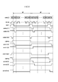
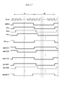
- FIG. 3 shows a signal timing diagram of the organic light emitting display according to the first exemplary embodiment of the present invention.
- FIG. 4A shows a select scan driver in the organic light emitting display according to the first exemplary embodiment of the present invention.
- FIG. 4B shows a flip-flop used in the select scan driver of FIG. 4A.
- FIG. 5 shows a signal timing diagram in the select scan driver of FIG. 4A.
- FIGs. 6, 9, and 11 show emit scan drivers in the organic light emitting displays according to second, third, and fourth exemplary embodiments of the present invention, respectively.
- FIG. 7 shows a schematic diagram of pixel areas of the organic light emitting display according to the second exemplary embodiment of the present invention.
- FIG. 8 shows a signal timing diagram of the organic light emitting display according to the second exemplary embodiment of the present invention.
- FIGs. 10 and 12 show signal timing diagrams in the emit scan drivers of FIGs. 9 and 11, respectively.
- FIGs. 13 and 14 show plan views of organic light emitting displays according to fourth and fifth exemplary embodiments of the present invention, respectively.
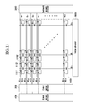
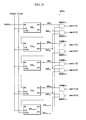
- FIGs. 15, 16, and 18 show emit scan drivers in the organic light emitting displays according to fifth, sixth, and seventh exemplary embodiments of the present invention, respectively.
- FIG. 17 shows a signal timing diagram in the emit scan driver of FIG. 16.
- FIGs. 19 and 20 show signal timing diagrams in the emit scan driver of FIG. 18, respectively.
- FIGs. 21 and 22 show plan views of organic light emitting displays according to eighth and ninth exemplary embodiments of the present invention, respectively.
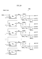
- FIGs. 23, 25, 26, and 28 show scan drivers in the organic light emitting displays according to ninth, tenth, eleventh, and twelfth exemplary embodiments of the present invention, respectively.
- FIGs. 24 and 27 show signal timing diagrams in the scan drivers of FIGs. 23 and 26, respectively.
- FIG. 29 shows a signal timing diagram in a scan driver according to a thirteenth exemplary embodiment of the present invention.
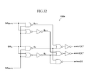
- FIGs. 30 and 32 show scan drivers in the organic light emitting displays according to fourteenth and fifteenth exemplary embodiments of the present invention, respectively.
- FIG. 31 shows a signal timing diagram in the scan driver of FIG. 30.
- FIG. 33 shows a plan view of an organic light emitting display according to a sixteenth exemplary embodiment of the present invention.
- FIG. 34 shows a signal timing diagram in a select scan driver according to a seventeenth exemplary embodiment of the present invention.
- an organic light emitting display includes a substrate (not shown) for forming a display panel, and the substrate is divided into a display area 100 seen as a screen to a user and a peripheral area surrounding the display area 100.
- the peripheral area includes a select scan driver 200, emit scan drivers 300, 400, and a data driver 500.
- the display area 100 includes a plurality of data lines D 1 to D n , a plurality of select scan lines S 1 to S m , a plurality of emit scan lines E 11 to E 1m and E 21 to E 2m , and a plurality of pixels.
- the data lines D 1 to D n are extended in a column direction and transmit data signals representing images to the corresponding pixels.
- the select scan lines S 1 to S m and the emit scan lines E 11 to E 1m and E 21 to E 2m are extended in a row direction and transmit select signals and emission control signals to the corresponding pixels, respectively.
- the pixel area 110 is defined by two adjacent scan lines S 1 to S m and two adjacent data lines D 1 to D m , and two pixels 111, 112 are formed on the pixel area 110. That is, two pixels 111, 112 of the pixel area 110 are coupled to one of the data lines D 1 to D m and one of the select scan lines S 1 and S m in common.
- the select scan driver 200 sequentially transmits select signals for selecting corresponding lines to the select scan lines S 1 to S m in order to apply data signals to pixels of the corresponding lines.
- the emit scan driver 300 sequentially transmits emission control signals for controlling light emission of pixels 111 to the emit scan lines E 11 to E 1m in one subfield
- the emit scan driver 400 sequentially transmits emission control signals for controlling light emission of pixels 112 to the emit scan lines E 21 to E 2m in the other subfield.
- the data driver 500 applies data signals corresponding to the pixels of lines to which select signals are applied to the data lines D 1 to D m each time the select signals are sequentially applied.
- the select and emit scan drivers 200, 300, 400 and the data driver 500 are coupled to the substrate.
- the select and emit scan drivers 200, 300, and/or 400 and/or the data driver 500 can be installed directly on the substrate, and they can be substituted with a driving circuit which is formed on the same layer on the substrate as the layer on which scan lines, data lines, and transistors are formed.
- the select and emit scan drivers 200, 300, and/or 400 and/or the data driver 500 can be installed in a chip format on a tape carrier package (TCP), a flexible printed circuit (FPC), or a tape automatic bonding unit (TAB) coupled to the substrate.
- TCP tape carrier package
- FPC flexible printed circuit
- TAB tape automatic bonding unit
- FIG. 2 shows a schematic diagram of the pixel areas of the organic light emitting display of FIG. 1.
- the three pixel areas 110 ij , 110 i(j+1) , 110 i(j+2) coupled to the scan line S i of the i th row (where 'i' is an positive integer less than 'm') and the data lines D j to D j+2 of the j th to (j+2) th columns (where 'j' is an positive integer less than 'n') will be exemplified in FIG. 2. It is assumed that the pixels are arranged in an order of red, green, and blue along the row direction in FIG. 2.
- the two pixels 111, 112 have one of the data lines D 1 to D n and a pixel driver in common, and the pixel driver includes a driving transistor M1, a switching transistor M2, and a capacitor Cst.
- the two pixels 111 ij , 112 ij of the pixel area 110 ij defined by the i th select scan line S i and the j th data line D j include the pixel driver, two emit transistors M31, M32, and two organic light emitting elements OLED1, OLED2.
- the organic light emitting elements OLED1, OLED2 emit light red and green lights, respectively.
- the organic light emitting elements emit light having a brightness corresponding to the applied current.
- the organic light emitting elements OLED1, OLED2 of the two pixels 111 i(j+1) , 112 i(j+1) emit light blue and red lights, respectively, and the organic light emitting elements OLED1, OLED2 of the two pixels 111 i(j+2) , 112 i(j+2) emit light green and blue lights, respectively.
- the driving transistor M1 has a source coupled to the power line VDD for supplying a power supply voltage, and has a gate coupled to a drain of the switching transistor M2, and a capacitor Cst is coupled between a source and a gate of the driving transistor M1.
- the switching transistor M2 having a gate coupled to the select scan line S i and a source coupled to the data line D j transmits the data signal converted to analog voltage (hereinafter, "data voltage”) provided by the data line D j in response to the select signal provided by the select scan line S i .
- the driving transistor M1 has a drain coupled to sources of emit transistors M31, M32, and gates of the emit transistors M31, M32 are coupled to the emission control signal lines E 1i , E 2i , respectively. Drains of the emit transistors M31, M32 are coupled, respectively, to anodes of the organic light emitting elements OLED1, OLED2, and a power supply voltage VSS is applied to cathodes of the organic light emitting elements OLED1, OLED2.
- the power supply voltage VSS in the first exemplary embodiment can be a negative voltage or a ground voltage.
- the switching transistor M2 transmits the data voltage provided by the data line D j to the gate of the driving transistor M1 in response to a low-level select signal provided by the select scan line S i , and the voltage which corresponds to a difference between the data voltage transmitted to the gate of the transistor M1 and the power supply voltage VDD is stored in the capacitor Cst.
- the emit transistor M31 is turned on in response to a low-level emission control signal provided by the emission control signal line E 1i , the current I OLED , which corresponds to the voltage stored in the capacitor Cst as expressed in Equation 1 below, is transmitted to the organic light emitting element OLED1 from the driving transistor M1 to emit light.
- the emitting transistor M32 when the emitting transistor M32 is turned on in response to a low-level emission control signal provided by the emission control signal line E 2i , the current which corresponds to the voltage stored in the capacitor Cst is transmitted to the organic light emitting element OLED2 from the driving transistor M1 to emit light.
- Two emission control signals applied to the low emission control signal lines E 1i , E 2i respectively have low-level periods without repetition during one field so that one pixel area can display two colors.
- I OLED ⁇ 2 (
- ⁇ is a constant determined by a channel width and a channel length of the transistor M1
- V SG is a voltage between source and gate of the transistor M1
- V TH is a threshold voltage of the transistor M1.
- FIG. 3 A driving method of the organic light emitting display according to the first exemplary embodiment of the present invention will be described in more detail with reference to FIG. 3.
- the select signal applied to the select scan line S i is depicted as 'select[i]'
- the emission control signals applied to the emit scan lines E 1i , E 2i are depicted as 'emit1[i]', 'emit2[i]', respectively.
- the data voltage data[j] applied to the data line D j is depicted in FIG. 3 since the data voltages are simultaneously applied to the data lines D 1 to D n .
- one field includes two subfields 1F, 2F, and the low-level select signals are sequentially applied to the select scan lines S 1 to S m in each subfield 1F or 2F.
- the two organic light emitting elements OLED1, OLED2 of the two pixels sharing the pixel driver emit light during periods corresponding to subfields SF1, SF2, respectively.
- a low-level select signal select[1] when a low-level select signal select[1] is applied to the select scan line S 1 on the first row, a data voltage data[j] corresponding to the organic light emitting element OLED1 of the each pixel area on the first row is applied to the corresponding data line D j , and a low-level emission control signal emit1[1] is applied to the emission control signal line E 1i on the first row.
- the emit transistor M31 of the pixel area on the first row is turned on, and a current corresponding to the data voltage data[j] is transmitted to the organic light emitting element OLED1 from the driving transistor M1 to thus emit light.
- the light is emitted during the period in which the emission control signal emit1[1] is low-level, and the low-level period of the emission control signal emit 1[1] is the same as the period which corresponds to the subfield 1F.
- the data voltages are sequentially applied to pixel areas of from the first to m th rows to emit the organic light emitting element OLED1.
- a low-level select signal select[i] is applied to the select scan line S i on the i th row
- the data voltage data[j] corresponding to the organic light emitting element OLED1 of the each pixel area of the i th row are applied to the corresponding data line D j
- a low-level emission control signal emit1[i] is applied to the emission control signal line E 1i of the i th row.
- a current corresponding to the data voltage data[j] provided by each of the data lines D j is accordingly supplied to the organic light emitting element OLED1 of the corresponding pixel area on the i th row to thus emit light during the period which corresponds to the subfield 1F. Therefore, in the subfield 1F, the pixel on which the organic light emitting element OLED1 is formed emits light in the two pixels which are adjacent in the row direction.
- a low-level select signal select[1] to select[m] is sequentially applied to the select scan lines S 1 to S m of from the first to the m th rows, and when the select signal select[i] is applied to the corresponding select scan line S i , the data voltage data[j] corresponding to the organic light emitting element OLED2 of each pixel area of the corresponding rows are applied, respectively, to the corresponding data lines D j .
- a low-level emission control signal emit2[i] is sequentially applied to the emission control signal line E 21 to E 2m in synchronization with sequentially applying the low-level select signal select[i] to the select scan lines S 1 to S m .
- a current corresponding to the applied data voltage is transmitted to the organic light emitting element OLED2 through the emitting transistor M32 in each pixel area to emit light.
- the low-level period of the emission control signal emit2[i] is the same as the period which corresponds to the subfield 2F. Therefore, in the subfield 2F, the pixel on which the organic light emitting element OLED2 is formed emits light in the two pixels which are adjacent in the row direction.
- one field is divided into two subfields, and the subfields are sequentially driven in the organic light emitting display driving method according to the first exemplary embodiment.
- One organic light emitting element of two pixels of one pixel area in each subfield emits light, and the two organic light emitting elements sequentially emit light through two subfields to thus represent colors.
- the number of data lines and the number of pixel drivers can be reduced since the two pixels share the data line D j and the pixel driver. As a result, the number of integrated circuits for driving the data lines can be reduced, and the elements can be easily arranged in the pixel area.
- FIG. 4A shows the select scan driver 200 in the organic light emitting display according to the first exemplary embodiment.
- FIG. 4B shows a flip-flop used in the select scan driver 200 of FIG. 4A.
- FIG. 5 shows a signal timing diagram in the select scan driver 200 of FIG. 4A.
- An inverted signal of a clock VCLK is depicted as VCLKb in FIG. 4A, which is not shown in FIG. 5.
- the low-level period of one clock VCLK cycle is the same as the high-level period of one clock VCLK cycle.
- the low-level pulse width of the select signal select[i] is the same as the half clock VCLK cycle in order to minimize the frequency of the clock VCLK; the number m of the select scan lines S 1 to S m is even, and the low-level pulse width of the emission control signal emit1[i] or emit2[i] corresponds to an integral multiple of 'm'; and a flip-flop used in the scan drivers 200, 300, 400 outputs a signal which is input during a half clock cycle during a one clock VCLK cycle. In these conditions, since the output pulse of the flip-flop is an integral multiple of one clock VCLK cycle, the output signal of the flip-flop may not be used as a select signal.
- the select scan driver 200 includes (m+1) flip-flops FF 11 to FF 1(m+1) and m NAND gates NAND 11 to NAND 1m as shown in FIG. 4A, and operates as a shift register.
- An output signal of the NAND gate NAND 1i is the select signal select[i] (where 'i' is a positive integer of less than 'm').
- the start signal VSP1 is input to the first flip-flop FF 11 in FIG. 4A, and the output signal SR 1i of the i th flip-flop FF 1i is input to the (i+1) th flip-flop FF 1(i+1) .
- the i th NAND gate NAND 1i performs a NAND operation to the output signals SR 1i , SR 1(i+1) of the two adjacent flip-flops FF 1i , FF 1(i+1) and outputs the select signal select[i].
- the clock VCLKb or VCLK inverted to the clock VCLK or VCLKb, which are used in the flip-flop FF 1i are used in the flip-flops FF 1(i+1) adjacent to the flip-flip FF 1i .
- the flip-flop FF 1i which is located at the odd-numbered position in the longitudinal direction uses the clocks VCLK, VCLKb as inner clocks clk, clkb, respectively, and the flip-flop FF 1i which is located at the even-numbered position in the longitudinal direction uses the clocks VCLKb, VCLK as inner clocks clk, clkb, respectively.
- the flip-flop FF 1i outputs an input signal in response to the high-level clock clk, and latches and outputs the input signal of the high-level clock clk in response to the low-level clock clk.
- the output signal SR 1(i+1) of the flip-flop FF 1(i+1) is shifted from the output signal SR 1i of the flip-flop FF 1i by the half clock VCLK cycle.
- the flip-flop FF 11 since the start signal VSP1 has a high-level pulse in the high-level period of the one clock VCLK cycle in the respective subfields 1F, 2F, the flip-flop FF 11 outputs the high-level pulse during one clock VCLK cycle in the respective subfields 1F, 2F. As a result, the flip-flops FF 11 to FF 1m may sequentially output each output signal SR 1i by shifting the high-level pulse by the half clock VCLK cycle.
- the NAND gate NAND 1i performs the NAND operation of the output signals SR 1i , SR 1(i+1) of the flip-flops FF 1i , FF 1(i+1) , and outputs a low-level pulse when both output signals SR 1i , SR 1(i+1) are high-level.
- the output signal SR 1(i+1) of the flip-flop FF 1(i+1) is shifted from the output signal SR 1i of the flip-flop FF 1i by the half clock VCLK cycle
- the output signal of the NAND gate NAND 1i has a low-level pulse in a period, i.e., the half clock cycle during which the both output signals SR 1i , SR 1(i+1) have the high-level pulse in common in the respective subfields 1F, 2F.
- the output signal select[i+1] of the NAND gate NAND 1(i+1) is shifted from the output signal select[i] of the NAND gate NAND 1i by half the clock VCLK cycle. Therefore, the select scan driver 200 may sequentially output each select signal select[i] by shifting the low-level pulse by the half clock VCLK cycle.
- the flip-flop FF 1i includes a clocked inverter 211, and an inverter 212 and a clocked inverter 213 for forming a latch.
- the clocked inverter 211 inverts an input signal (in) when the clock clk is high-level, and the inverter 212 inverts the output signal of the clocked inverter 211.
- the clock clk is low-level
- the output of the clocked inverter 211 is blocked, the output signal of the inverter 212 is input to the clocked inverter 213, and the output signal of the clocked inverter 213 is input to the inverter 212.
- the latch is formed.
- the output signal (out) of the inverter 212 is the output signal of the flip-flop FF 1i
- the input signal (inv) of the inverter 212 is the inverted signal to the output signal (out). Therefore, the flip-flop FF 1i can output the input signal (in) when the clock (clk) is high-level, and latch and output the input signal (in) in the high-level period of the clock (clk) when the clock (clk) is low-level.
- FIG. 6 shows an emit scan driver 300 or 400 in the organic light emitting display according to the first exemplary embodiment.
- the emit scan driver 300 includes m flip-flops FF 21 to FF 2m , and operates as a shift register.
- the emit scan driver 300 use a clock the same as the clock VCLK of the select scan driver 200.
- a start signal VSP2 is input to the first flip-flop FF 21
- the output signal of the i th flip-flop FF 2i is the emission control signal emitl[i] of the i th emission control signal line E 1i , and is input to the (i+1) th flip-flop FF 2(i+1) .
- a falling edge of a low-level pulse in the emission control signal emit1[1] of the first flip-flop FF 21 is shifted from a rising edge of a high-level pulse in the output signal SR 11 of the first flip-flop FF 11 . Therefore, differently from FIG.
- the flip-flop FF 2i which is located at the odd-numbered position in the longitudinal direction uses the clocks VCLKb, VCLK as inner clocks clk, clkb, respectively, and the flip-flop FF 2i which is located at the even-numbered position in the longitudinal direction uses the clocks VCLK, VCLKb as inner clocks clk, clkb, respectively.
- the flip-flop FF 2i has the same structure as the flip-flop FF 1i described in FIGs. 4A and 4B.
- the output signal emit1[1] of the flip-flop FF 21 has a low-level pulse in the subfield 1F.
- the output signal emit 1[1] of the flip-flop FF 21 has a high-level pulse in the subfield 2F.
- the emit scan driver 300 can sequentially output each emission control signal emit1[i], which has the low-level pulse in a period which corresponds to the subfield 1F, by shifting the half clock VCLK cycle.
- the low-level period is shorter than the period which corresponds to the subfield 1F, the low-level period becomes shorter than the period which corresponds to the subfield 1F.
- the emit scan driver 400 may have the same structure as the emit scan driver 300.
- a signal which is shifted from the start signal VSP2 by the period corresponding to the subfield 1F, may be used as a start signal of the emit scan driver 400.
- the emit scan driver can sequentially output the each emission control signal emit2[i] by shifting the half clock VCLK cycle as shown in FIG. 3.
- the falling edge of the select signal select[i] in the respective subfields 1F, 2F corresponds to the falling edge of the respective emission control signals emit1[i], emit2[i] transmitted to the emission control signal lines E 1i , E 2i .
- the select signal select[i] and emission control signals emit1[i], emit2[i] may be used for the organic light emitting display using the voltage programming method.
- the current from the driving transistor M1 needs to be blocked from the organic light emitting elements OLED1, OLED2 when the corresponding data signal are programmed to the pixel.
- FIG. 7 shows a schematic diagram of the pixel areas of the organic light emitting display according to a second exemplary embodiment of the present invention.
- the organic light emitting display according to a second exemplary embodiment uses the current programming method in which the data signals converted to the analog currents (hereinafter, "data currents") are applied to the data lines D 1 to D n .
- the pixel areas 110' ij , 110' i(j+1) , 110' i(j+2) according to the second exemplary embodiment have the same structure as that according to the first exemplary embodiment except for a pixel driver.
- the pixel driver includes a driving transistor M1', a switching transistor M2', a diode-connecting transistor M4, and a capacitor Cst'.
- the connecting structure of the transistors M1', M2', M31', M32', the capacitor Cst', the select scan line S i , the emit scan lines E 1i , E 2i , and the data line D j are the same as those described in FIG. 2.
- the transistor M4 is coupled between the drain of the transistor M1' and the data line D j
- the gate of the transistor M4 is coupled to the select scan line S i .
- the transistors M2', M4 are turned on and the data current provided by the data line D j flows to the drain of the transistor M1' in response to a low-level select signal provided by the select scan line S i . Then, the capacitor Cst' is charged until a current flowing to the drain of the transistor M1' by the voltage stored in the capacitor Cst' corresponds to the data current. That is, the voltage corresponding to the data current is stored in the capacitor Cst'.
- the emit transistor M31' When the emit transistor M31' is turned on in response to a low-level emission control signal emit1[i]' provided by the emission control signal line E 1i , the current I OLED which corresponds to the voltage stored in the capacitor Cst' is transmitted to the organic light emitting element OLED1' from the driving transistor M1' to emit light.
- the emitting transistor M32' is turned on in response to a low-level emission control signal emit2[i]' provided by the emission control signal line E 2i , the current which corresponds to the voltage stored in the capacitor Cst' is transmitted to the organic light emitting element OLED2' from the driving transistor M1' to emit light.
- one field is divided into the two subfields 1F, 2F, and the driving method according to the second exemplary embodiment is the same as that according to the first exemplary embodiment except for the timing of the emission control signals emit1[i]', emit2[i]'.
- the emission control signal emit1[i]' transmitted to the i th emission control signal line E 1i has the low-level pulse after the select signal select[i] transmitted to the i th select scan line S i rises to the high-level.
- the emission control signal emit1[i]' has the low-level pulse during a period which corresponds to a difference between the subfield 1F and the low-level pulse width of the select signal select[i].
- a low-level emission control signal emit1[i]' is applied to the emission control signal line E 1i on the first row.
- the emit transistor M31' of the pixel area on the i th row is turned on, and a current corresponding to the voltage stored in the capacitor Cst' is transmitted to the organic light emitting element OLED1 to thus emit light.
- the low-level select signals select[1] to select[m] are sequentially applied to the select scan lines S 1 to S m of from the first to the m th rows.
- the select signal select[i] of the select scan line S i rises to the high-level
- the low-level emission control signal emit1[i]' is applied to the emit scan line E 1i on the i th row.
- the emission control signal emit2[i]' transmitted to the i th emission control signal line E 2i has the low-level pulse after the select signal select[i] transmitted to the i th select scan line S i rises to the high-level.
- the emission control signal emit1[i]' has the low-level pulse during a period which corresponds to a difference between the subfield 2F and the low-level pulse width of the select signal select[i].
- emit scan drivers 300a, 400a for generating the waveforms shown in FIG. 8 will be described with reference to FIGs. 9 to 12.
- FIG. 9 shows the emit scan driver 300a in the organic light emitting display according to the second exemplary embodiment
- FIG. 10 shows a signal timing diagram of the emit scan driver 300a shown in FIG. 9.
- the select scan driver 200 shown in FIGs. 4A and 4B may be used as the select scan driver according to the second exemplary embodiment.
- the emission control signal emit1[i]' is the high-level when the select signal select[i] is the low-level, the low-level pulse width of the emission control signal emit1[i]' becomes an odd multiple of the half clock cycle.
- the output signal of the emit scan driver 300 shown in FIG. 6 is an integral multiple of the one clock cycle, the emit scan driver 300 shown in FIG. 6 may not be applicable to the signal timing diagram shown in FIG. 8.
- the emit scan driver 300a includes (m+1) flip-flops FF 31 to FF 3(m+1) and m NAND gates NAND 31 to NAND 3m , and operates as a shift register.
- a start pulse VSP2a shown in FIGs. 8 and 10 is input to first flip-flop FF 31 , and an output signal SR 3i of i th the flip-flop FF 3i is input to the (i+1) th flip-flop FF 3(i+1) (where 'i' is an positive integer less that 'm').
- the NAND gate NAND 3i performs NAND operation between the output signals SR 3i , SR 3(i+1) of the two flip-flops FF 3i , FF 3(i+1) , and outputs the emission control signal emit1[i]'.
- the emit scan driver 300a has the same structure as that shown in FIG. 4A except for the clocks VCLK, VCLKb. That is, the flip-flop FF 3i which is located at the odd number of position in the longitudinal direction uses the clocks VCLKb, VCLK as inner clocks clk, clkb, respectively, and the flip-flop FF 3i which is located at the even number of position uses the clocks VCLK, VCLKb as inner clocks clk, clkb, respectively. Then, the falling edge of the low-level pulse in the emission control signal emit1[i]' can be shifted by the half clock VCLK cycle from the falling edge of the low-level pulse in the select signal select[i].
- the first flip-flop FF 31 receives the start signal VSP2a when the clock VCLK is the low-level, and outputs the received signal during the one clock VCLK cycle.
- the start signal VSP2a has the high-level pulse in the low-level period of all clock VCLK cycles in the subfield 1F, and has the low-level pulse in the low-level period of all clock VCLK cycles in the subfield 2F. Therefore, the flip-flops FF 31 to FF 3(m+1) may sequentially output the output signals, which respectively have the high-level pulses in a period which corresponds to the subfield 1F, by shifting the half clock VCLK cycle.
- the NAND gate NAND 3i performs NAND operation between the output signals SR 3i , SR 3(i+1) of the flip-flops FF 3i , FF 3(i+1) , and outputs the low-level pulse while the both output signals SR 3i , SR 3(i+1) are the high-level. Therefore, the output signal of the NAND gate NAND 3i , i.e. the emission control signal emit1[i]' has the low-level pulse during a period which corresponds to a difference the subfield 1F and the half clock VCLK cycle. The falling edge of the emission control signal emit1[i]' corresponds to the rising edge of the select signal select[i]. In addition, as shown in FIGs.
- the emission control signal emit1[i+1]' which is the output signal of the NAND gate NAND 3(i+1) is shifted by the half clock VCLK cycle from the emission control signal emit1[i]' which is the output signal of the NAND gate NAND 3i .
- the emit scan driver 300a may be applicable to the emit scan driver 400a.
- the period corresponding to the subfield 1F is the same as the period corresponding to the subfield 2F, a signal shifted by the subfield 1F from the start signal VSP2a can be used as a start signal VSP3a of the emit scan driver 400a.
- the emit scan drivers 300a, 400a have the same structure as the select scan driver 200 shown in FIGs. 4A and 4B, but further embodiments may have a different structure from that of select scan driver 200. These further embodiments will be described in more detail with reference to FIGs. 11 and 12.
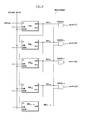
- FIG. 11 shows an emit scan driver 300b in an organic light emitting display according to a third exemplary embodiment
- FIG. 12 shows a signal timing diagram of the emit scan driver 300b shown in FIG. 11.
- the emit scan driver 300b includes (m+1) flip-flops FF 41 to FF 4(m+1) and m NOR gates NOR 41 to NOR 4m , and operates as a shift register.
- An output signal of the NOR gate NOR 4i is the emission control signal emit[1]' transmitted to the emit scan line E 1i .
- a start pulse VSP2b shown in FIG. 12 is input to first flip-flop FF 41 , and an output signal SR 4i of i th the flip-flop FF 4i is input to the (i+1) th flip-flop FF 4(i+1) (where 'i' is an positive integer less that 'm').
- the NOR gate NOR 4i performs a NOR operation between the output signals SR 4i , SR 4(i+1) of the two flip-flops FF 4i , FF 4(i+1) , and outputs the emission control signal emit [i]'.
- the emission control signal emit1[i]' is generated by a NOR operation.
- the output signal SR 4i of the flip-flop FF 4i is shifted by the half clock VCLK cycle from the output signal SR 3i of the flip-flop FF 3i . Therefore, the flip-flop FF 4i uses the clock VCLK or VCLKb inverted to the clock VCLKb or VCLK of the flip-flop FF 3i shown in FIG. 9, and the first flip-flop FF 41 receives the start signal VSP2b when the clock VCLK is the high-level and outputs the received signal during the one clock VCLK cycle. As shown in FIG.
- the output signal SR 41 of the flip-flop FF 41 has the high-level pulse during this period.
- the output signal SR 41 is the low-level in the subfield 2F.
- the flip-flops FF 41 to FF 4(m+1) may sequentially output the output signals SR 41 to SR 4(m+1) by shifting the high-level pulse by the half clock VCLK cycle, and the respective output signals SR 41 to SR 4(m+1) have the high-level pulse in the period which corresponds to the difference between the subfield 1F and the one clock VCLK cycle.
- NOR gate NOR 4i outputs the low-level pulse while at least one of the output signals SR 4i , SR 4(i+1) of the flip-flops FF 4i , FF 4(i+1) is the high-level. Therefore, the output signal emit1[i]' has the low-level pulse in a period which corresponds to a difference between the subfield and the half clock VCLK cycle, and the falling edge of the low-level pulse corresponds to the rising edge of the select signal select[i]. In addition, the output signal emit1[i+1]' is shifted from the emission control signal emit1[i]' by the half clock VCLK cycle since the output signal SR 4(i+1) is shifted from the output signal SR 4i by the half clock VCLK cycle.
- the emit scan driver 300b may be applicable to the emit scan driver 400b.
- the period corresponding to the subfield 1F is the same as the period corresponding to the subfield 2F, a signal shifted by the subfield 1F from the start signal VSP2b can be used as a start signal of the emit scan driver 400b.
- the emit scan driver used in the organic light emitting display of the current programming method may be applicable to that of the voltage programming method. That is, the emit scan driver according to the second and third exemplary embodiments may be applicable to the organic light emitting display in which the organic light emitting elements doesn't emit light in the low-level period of the select signal.
- select and emit scan drivers according to the first to third exemplary embodiment may be applicable to an organic light emitting display shown in FIG. 13.
- FIG. 13 shows a plan view of the organic light emitting display according to a fourth exemplary embodiment of the present invention.
- a connection between the emit scan lines E 1i , E 2i on the i th row and the pixel area 110' is different from a connection between the emit scan lines E 1(i+1) , E 2(i+1) on the (i+1) th row and the pixel area 110'.
- the emit scan line E 1i is coupled to the left pixels 111' of the pixel areas 110' on the i th row (where 'i' is an odd integer less than 'm') and the emit scan line E 2i is coupled to the right pixels 112' of the pixel areas 110' on the i th row
- the emit scan line E 1(i+1) is coupled to the right pixels 112' of the pixel areas 110' on the (i+1) th row
- the emit scan line E 2(i+1) is coupled to the left pixels 112' of the pixel areas 110' on the (i+1) th row.
- the left pixels 111' of the pixel areas 110' on the odd row and the right pixels 112' of the pixel areas 110' on the even row emit light in the subfield 1F
- the right pixels 112' of the pixel areas 110' on the odd row and the left pixels 111' of the pixel areas 110' on the even row emit light in the subfield 2F.
- FIG. 14 shows a plan view of an organic light emitting display according to a fifth exemplary embodiment of the present invention.
- the organic light emitting display according to the fifth exemplary embodiment has the same structure as that shown in FIG. 1 except for an emit scan driver 600 in place of emit scan drivers 300, 400.
- the emit scan driver 600 sequentially transmits emission control signals emit1[1] to emit1[m] for controlling light emission of pixels 111 to the emit scan lines E 11 to E 1m in the subfield 1F, and sequentially transmits emission control signals emit2[1] to emit2[m] for controlling light emission of pixels 112 to the emit scan lines E 21 to E 2m in the subfield 2F.
- the emit scan driver 600 for generating the signal timing shown in FIG. 3 will be described with reference to FIG. 15.
- the emit scan driver 600 may output one, for example emit1[i], of the emission control signals emit1[i], emit2[i] as does the emit scan driver 300 shown in FIG. 6, and invert the emission control signal emit1[i] to output the emission control signal emit2[i].
- the emit scan driver 600 includes m flip-flops FF 5l to FF 5m and m inverters INV 5l to INV 5m , and operates as a shift register.
- the clock VCLK shown in FIG. 3 is input to the emit scan driver 600.
- the flip-flop FF 5i has the same connection and structure as the flip-flop FF 2i shown in FIG. 6.
- the start signal VSP2 shown in FIG. 3 is input to the flip-flop FF 5l .
- An output signal of the i th flip-flop FF 5i becomes the emission control signal emit1[i] of the emission control signal line E 1i on the i th row, an input signal of the (i+1) th flip-flop FF 5(i+1) , and an input signal of the i th inverter INV 5i .
- An output signal of the i th inverter INV 5i is the emission control signal emit2[i] of the emission control signal line E 2i on the i th row, and the emission control signal emit2[i] is inverted to the emission control signal emit1[i] by the inverter INV 5i .
- the emit scan driver 600 can sequentially output the emission control signals emit1[1] to emit1[m], which respectively have the low-level pulses in a period which corresponds to the subfield 1F, by shifting the half clock VCLK cycle.
- the emit scan driver 600 inverts the emission control signals emit1[1] to emit1[m] to thus sequentially output the emission control signals emit2[1] to emit2[m], which respectively have the low-level pulses in a period which corresponds to the subfield 2F, by shifting the half clock VCLK cycle.
- the input signal of the inverter 212 since the input signal of the inverter 212 is inverted to the output signal (out), the input signal of the inverter 212 can be an inverted output signal (inv) of the flip-flop. Therefore, the inverted output signal (inv) can be used as the emission control signal emit2[i], and the inverter INV 5i can be eliminated in the emit scan driver 600.
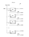
- FIG. 16 shows the emit scan driver 600a in an organic light emitting display according to a sixth exemplary embodiment
- FIG. 17 shows a signal timing diagram of the emit scan driver 600a shown in FIG. 16.
- the emit scan driver 600a may generate one, for example, emit1[i]' of the emission control signals emit1[i]', emit2[i]' as does the emit scan driver 300a shown in FIG. 9, and may generate the emission control signal emit2[i] from the emission control signal emit 1[i].
- the emit scan driver 600a includes (m+1) flip-flops FF 6l to FF 6(m+1) , m NAND gates NAND 6l to NAND 6m , m NOR gates NOR 6l to NOR 6m , and m inverters INV 6l to INV 6m , and operates as a shift register.
- the clock VCLK shown in FIG. 3 is input to the emit scan driver 600.
- An output signal of the i th NAND gate NAND 6i is the emission control signal emit1[i]' of the emission control signal line E 1i on the i th row, and a signal which is inverted to an output signal NOR gate NOR 6i by the inverter INV 6i is the emission control signal emit2[i]' of the emission control signal line E 2i on the i th row.
- the flip-flop FF 5i and the NAND gate NAND 6i have the same connection and structure as the flip-flop FF 2i and the NAND gate NAND 2i shown in FIG. 9.
- the start signal VSP2a shown in FIGs. 8 and 17 is input to the flip-flop FF 6l .
- the NAND gates NAND 6l to NAND 6m can sequentially output the emission control signals emit1[i]' to emit1[m]', which respectively have the low-level pulses in a period which corresponds to a difference between the subfield 1F and the half clock VCLK cycle, by shifting the half clock VCLK cycle.
- the NOR gate NOR 6i performs a NOR operation between the output signal SR 6i , SR 6(i+1) of the flip-flops FF 6i , FF 6(i+1) to output an output signal to the inverter INV 6i .
- the NOR gate NOR 6i and the inverter INV 6i operate as an OR gate.
- the output signal SR 6i of the flip-flops FF 6i has the low-level pulse in a period which corresponds to the subfield 2F, and the NOR gate NOR 6i outputs the high-level pulse while both the output signal SR 6i , SR 6(i+1) of the flip-flops FF 6i , FF 6(i+1) are the low level. Accordingly, the output signal of the NOR gate NOR 6i has the high-level pulse in a period which corresponds to a difference between the subfield 2F and the half clock VCLK cycle, and the inverter INV 6i inverts the output signal of the NOR gate NOR 6i to output the emission control signal emit2[i]'.
- the emission control signals emit2[1]' to emit2[m]' can be sequentially output by being shifted by the half clock VCLK cycle.
- the emission control signals emit1[i]', emit2[i]' are generated by a NAND operation and a NOR operation, respectively, but the emission control signal emit2[i]' may be generated by a NAND operation.
- the emission control signal emit2[i]' in the subfield 2F has the waveform shifted from the emission control signal emit1[i]', and the output signal SR 6i of the flip-flop FF 6i in the subfield 2F has the waveform inverted to the waveform of the output signal SR 6i in the subfield 1F. Therefore, the emission control signal emit2[i]' can be generated from a NAND operation of a signal inverted to the output signal SR 6i .
- This exemplary embodiment will be described with reference to FIGs. 18 and 19.
- FIG. 18 shows an emit scan driver 600b in an organic light emitting display according to a seventh exemplary embodiment
- FIG. 19 shows a signal timing diagram of the emit scan driver 600b shown in FIG. 18.
- the emit scan driver 600b has the same structure as the emit scan driver 600a shown in FIG. 16 except for the NAND gate NAND 5i .
- the emit scan driver 600b includes the flip-flops FF 6l to FF 6(m+1) and the NAND gates NAND 6l to NAND 6m shown in FIG. 16, and includes m NAND gates NAND 5l to NAND 5m instead of the NOR gates NOR 6l to NOR 6m and the inverters INV 6l to INV 6m .
- the input signal (inv) of the inverter 212 since the input signal (inv) of the inverter 212 is inverted to the output signal of the flip-flop FF 6i , the input signal (inv) becomes an inverted output signal /SR 6i of the flip-flop FF 6i .
- the NAND gate NAND 5i performs a NAND operation between the inverted output signals /SR 6i , /SR 6(i+1) of the flip-flops FF 6i , FF 6(i+1) to output the emission control signal emit2[i]'.
- the emission control signal emit2[i]' which is the output signal of the NAND gate NAND 5i has the signal timing shown in FIGs. 8 and 19.
- the emission control signal emit1[i]' has the low-level pulse in the period which corresponds to the difference between the subfield 1F and the half clock VCLK cycle.
- the low-level period of the emission control signal emit1[i]' can be controlled by changing the input signals of the NAND gate and/or NOR gate as shown in FIG. 20.
- the output signals SR 6(i-1) , SR 6(i+1) of the (i-1) th and (i+1) th flip-flops FF 6(i-1) , FF 6(i+1) are input to the i th NAND gate NAND 6i and the i th NOR gate NOR 6i shown in FIG. 16.
- the emission control signal emit1[i]" has the low-level pulse in a period which corresponds to a difference between the subfield 1F and the one clock VCLK cycle
- the emission control signal emit2[i]" has the low-level pulse in a period which corresponds to a difference between the subfield 2F and the one clock VCLK cycle.
- FIG. 21 shows a plan view of the organic light emitting display according to an eighth exemplary embodiment of the present invention.
- the emit scan line E 1i is coupled to the left pixels 111' of the pixel areas 110' on the i th row (where 'i' is an odd integer of less than 'm') and the emit scan line E 2i is coupled to the right pixels 112' of the pixel areas 110' on the i th row, and the emit scan line E 1(i+1) is coupled to the right pixels 112' of the pixel areas 110' on the (i+1) th row and the emit scan line E 2(i+1) is coupled to the left pixels 112' of the pixel areas 110' on the (i+1) th row.
- the emit scan lines E 1i , E 2i , E 1(i+1) , E 2(i+1) are coupled to the emit scan driver 600.
- FIG. 22 shows a plan view of the organic light emitting display according to a ninth exemplary embodiment of the present invention.
- the organic light emitting display according to the ninth exemplary embodiment has the same structure as that shown in FIGs. 1 and 14 except for a scan driver 700 sharing the select scan driver and the emit scan driver.
- the scan driver 700 sequentially transmits select signals select[1] to select[m] for selecting corresponding lines to the select scan lines S 1 to S m in the subfields 1F and 2F.
- the scan driver 700 sequentially transmits emission control signals emit1[1] to emit1[m] for controlling light emission of pixels 111 to the emit scan lines E 11 to E 1m in the subfield 1F, and sequentially transmits emission control signals emit2[1] to emit2[m] for controlling light emission of pixels 112 to the emit scan lines E 21 to E 2m in the subfield 2F.
- the scan driver can generate both emission control signals emit1[i], emit2[i]. Therefore, the method for generating the select signal select[i] from this scan driver will be described below.
- FIG. 23 shows the scan driver 700 in the organic light emitting display according to the ninth exemplary embodiment
- FIG. 24 shows a signal timing diagram of the scan driver 700 shown in FIG. 23.
- the emission control signal emit2[i] is inverted to the emission control signal emit1[i], and the select signal select[i] has the low level in a period in which the level of the emission control signal emit1[i] is different from that of the emission control signal emit1[i+1]. Therefore, the scan driver 700 can generate the select signal [i] and the emission control signals emit1[i], emit2[i].
- the scan driver 700 includes (m+1) flip-flops FF 7l to FF 7(m+1) , m XNOR gate XNOR 7l to XNOR 7m , and m inverters INV 7l to INV 7m , and operates as a shift register.
- an XOR gate and an inverter may be used as the XNOR gate.
- the clock VCLK and the start signal VSP2 shown in FIG. 15 are input to the scan driver 700.
- the flip-flop FF 5i and the inverter INV 7i have the same connection and structure as the flip-flop FF 5i and the inverter INV 5i shown in FIG. 15. Therefore, an output signal SR 7i of the flip-flop FF 7i is the emission control signal emit1[i], and a signal which is inverted to the output signal SR 7i of the flip-flop FF 7i by the inverter INV 7i is the emission control signal emit2[i].
- the XNOR gate XNOR 7i performs XNOR operation between the output signals SR 7i , SR 7(i+1) of the flip-flops FF 7i , FF 7(i+1) to output the select signal select[i]. That is, the XNOR gate XNOR 7i outputs the low-level select signal select[i] while the output signals SR 7i , SR 7(i+1) of the flip-flops FF 7i , FF 7(i+1) have the different levels.
- the output signal SR 7(i+1) of the flip-flop FF 7(i+1) is shifted from the output signal SR 7i of the flip-flop FF 7i by the half clock VCLK cycle. Therefore, the output signal select[i] of the XNOR gate XNOR 7i has the low-level pulse during the half clock VCLK cycle in the respective subfields 1F, 2F. The falling edges of the low-level pulses in the select signal select[i] respectively correspond to the falling edge and the rising edge of the output signal SR 7i of the flip-flop FF 7i . In addition, since the output signal SR 7(i+1) is shifted from the output signal SR 7i by the half clock VCLK cycle, the select signal select[i+1] is shifted from the select signal select[i] by the half clock VCLK cycle.
- the inverted output signal /SR 7i is output from the flip-flop FF 7i , the inverted output signal /SR 7i can be used as the emission control signal emit2[i].
- FIG. 25 shows a scan driver 700a in an organic light emitting display according to a tenth exemplary embodiment.
- the scan driver 700a has the same structure as that shown in FIG. 23 except for the inverter INV 7i .
- the output signal SR 7i and the inverted output signal /SR 7i of the flip-flop FF 7i correspond to the emission control signals emit1[i] and emit2[i], respectively.
- FIG. 26 shows the scan driver 700b in an organic light emitting display according to an eleventh exemplary embodiment
- FIG. 27 shows a signal timing diagram of the scan driver 700b shown in FIG. 26.
- the scan driver 700b includes (m+1) flip-flops FF 8l to FF 8(m+1) , m XNOR gates XNOR 8l to XNOR 8m , m NAND gates NAND 8l to NAND 8m , m NOR gates NOR 8l to NOR 8m , and m inverters INV 8l to INV 8m , and operates as a shift register.
- the clock VCLK and the start signal VSP2a shown in FIG. 17 are input to the scan driver 700b.
- the flip-flop FF 8i , the NAND gate NAND 8i , the NOR gate NOR 8i and the inverter INV 8i have the same connection and structure as the flip-flop FF 6i , the NAND gate NAND 6i , the NOR gate NOR 6i and the inverter INV 6i shown in FIG. 16. Accordingly, the NAND gate NAND 8i performs NAND operation between the output signals SR 8i , SR 8(i+1) of the flip-flops FF 8i , FF 8(i+1) to output the emission control signal emit1[i]' as shown in FIG. 27.
- the NOR gate NOR 8i performs a NOR operation between the output signals SR 8i , SR 8(i+1) of the flip-flops FF 8i , FF 8(i+1) to output an output signal to the inverter INV 8i , and the inverter INV 8i inverts the signal input from the NOR gate NOR 8i to output the emission control signal emit2[i]' as shown in FIG. 27.
- the flip-flop FF 8i and the XNOR gate XNOR 8i have the same connection as the flip-flop FF 7i and the XNOR gate XNOR 7i shown in FIG. 23. Therefore, the XNOR gate XNOR 8i performs the output signals SR 8i , SR 8(i+1) of the flip-flops FF 8i , FF 8(i+1) to output the select signal select[i].
- the scan driver 700b uses the start signal VSP2a which is inverted to the start signal VSP2 shown in FIG. 24. However, the scan driver 700b may use the start signal VSP2 shown in FIG. 24. Then, since the output signal of the flip-flop FF 8i is inverted to the output signal SR 8i shown in FIG. 27, the output signal of the NAND gate NAND 8i corresponds to the emission control signal emit2[i]' and the output signal of the inverter INV 8i corresponds to the emission control signal emit [i]'.
- the scan driver 700b may use the inverted output signal of the flip-flop FF 8i . That is, a NAND gate may be used instead of the NOR gate NOR 8i and the inverter INV 8i , and the NAND gate may perform a NAND operation between the inverted output signals of the flip-flops FF 8i , FF 8(i+1) to output the emission control signal emit2[i]'.
- the select signal select[i] may be generated from the emission control signals emit1[i]', emit2[i]'. This exemplary embodiment will be described with reference to FIG. 28.
- FIG. 28 shows a scan driver 700c in an organic light emitting display according to a twelfth exemplary embodiment.
- the scan driver 700c has the same structure as the scan driver 700b shown in FIG. 26 except for a NAND gate NAND 9i for generating the select signal select[i].
- the NAND gate NAND 9i performs a NAND operation between the emission control signals emit1[i]', emit2[i]' to output the select signal select[i].
- both emission control signals emit1[i]', emit2[i]' are high level in the low-level period of the select signal select[i] and one of the emission control signals emit1[i]', emit2[i]' is low level in the high-level period of the select signal select[i].
- the output signal of the NAND gate NAND 9i is the low-level while the both emission control signals emit1[i]', emit2[i]' are the high-level, the output signal of the NAND gate NAND 9i can be used as the select signal select[i].
- NOR gate NOR 8i may be used instead of the NOR gate NOR 8i and the inverter INV 8i .
- the low-level periods of the emission control signals emit1[i]', emit2[i]' may be controlled, as shown in FIG. 20. These exemplary embodiments will be described with reference to FIGs. 29 to 32.
- FIG. 29 shows a signal timing diagram of the scan driver 700b in an organic light emitting display according to the thirteenth exemplary embodiment.
- the output signals SR 8(i-1) , SR 8(i+1) of the (i-1) th and (i+1) th flip-flops FF 8(i-1) , FF 8(i+1) are input to the i th NAND gate NAND 8i and the i th NOR gate NOR 8i shown in FIG. 26.
- the emission control signal emit1[i]" has the low-level pulse in a period which corresponds to a difference between the subfield 1F and the one clock VCLK cycle
- the emission control signal emit2[i]" has the low-level pulse in a period which corresponds to a difference between the subfield 2F and the one clock VCLK cycle.
- the output signals SR 8(i-j) , SR 8(i+k) of the (i-j) th and (i+k) th flip-flops FF 8(i-j) , FF 8(i+k) (where 'j' and 'k' are respectively positive integers) are input to the i th NAND gate NAND 8i and the i th NOR gate NOR 8i , the low-level periods of the emission control signals emit1[i]", emit2[i]" may be controlled by the integral multiple of the half clock VCLK cycle.
- FIG. 30 shows a scan driver 700d in an organic light emitting display according to a fourteenth exemplary embodiment
- FIG. 31 shows a signal timing diagram of the scan driver 700d shown in FIG. 31.
- the signals SR 8(i-1) , SR 8i ,, SR 8(i+1) are the output signals of the flip-flops FF 8(i-1) , FF 8i ,, FF 8(i+1) in the scan driver 700b of FIG. 26, respectively.
- two signals A i , B i correspond to the emission control signals emit1[i]', emit2[i]' of the scan driver 700b, respectively.
- the NAND operation of the output signals SR 8(i-1) , SR 8i of the flip-flops FF 8(i-1) , FF 8i is performed by a NAND gate so that the signal A i-1 is output.
- the signal A i-1 has the low-level pulse in a period which corresponds to the subfield 1F and the half clock VCLK cycle, and corresponds to the emission control signal emit1[i-1]' shown in FIG. 27.
- the OR operation of the output signals SR 8(i-1) , SR 8i of the flip-flops FF 8(i-1) , FF 8i is performed by a NAND gate and an inverter so that the signal B i-1 is output.
- the signal B i-1 has the low-level pulse in a period which corresponds to the subfield 2F and the half clock VCLK cycle, and corresponds to the emission control signal emit2[i-1]' shown in FIG. 27.
- the signals A i , B i respectively correspond to the emission control signals emit1[i]', emit2[i]' shown in FIG. 27, and are respectively shifted from the signals A i-1 , B i-1 by the half clock VCLK cycle.
- the OR operation of the signals A i-1 , A i is performed by a NAND gate and an inverter so that the emission control signal emit1[i]" is output, and the emission control signal emit1[i]” has the low-level pulse while both signals A i-1 , A i are low level.
- the OR operation of the signals B i-1 , B i is performed by a NAND gate and an inverter so that the emission control signal emit2[i]" is output, and the emission control signal emit2[i]” has the low-level pulse while both signals B i-1 , B i are low level.
- the XNOR operation of the output signals SR 8i , SR 8(i+1) of the flip-flops FF 8i , FF 8(i+1) is performed so that the select signal select[i] is output.
- the low-level periods of the emission control signals emit1[i]", emit2[i]" may be controlled by the integral multiple of the half clock VCLK cycle.
- the select signal select[i] can be generated by a NAND gate in FIG. 30. This exemplary embodiment will be described with reference to FIG. 32.
- FIG. 32 shows a scan driver 700e in an organic light emitting display according to a fifteenth exemplary embodiment.
- the NAND operation of the output signal A i of the i th NAND gate and the output signal B i of the i th inverter is performed so that the select signal select[i] is output as shown in FIG. 28.
- FIG. 33 shows a plan view of the organic light emitting display according to a sixteenth exemplary embodiment of the present invention.
- the emit scan line E 1i is coupled to the left pixels 111' of the pixel areas 110' on the i th row (where 'i' is an odd integer of less than 'm') and the emit scan line E 2i is coupled to the right pixels 112' of the pixel areas 110' on the i th row, the emit scan line E 1(i+1) is coupled to the right pixels 112' of the pixel areas 110' on the (i+1) th row and the emit scan line E 2(i+1) is coupled to the left pixels 112' of the pixel areas 110' on the (i+1) th row.
- the emit scan lines E 1i , E 2i , E 1(i+1) ,, E 2(i+1) are coupled to the scan driver 700.
- a clip signal CLIP may be input to the NAND gate NAND 4i shown in FIG. 4A.
- the clip signal CLIP has a cycle corresponding to the half clock VCLK cycle, and has the low-level pulse whose width is shorter than the half clock VCLK cycle.
- the low-level period of the clip signal CLIP includes the falling edge or the rising edge of the clock VCLK.
- the low-level pulse width of the select signal select[i]' becomes shorter than the half clock VCLK cycle. That is, the falling edge of the select signal select[i]' is apart from the rising edge of the select signal select[i-1]' by the low-level pulse width of the clip signal CLIP.
- the case in which the select signal and the emission control signals provided by the scan drivers 200, 300, 400, 600, and/or 700 are directly applied to the select line and the emit lines is shown, but buffers may be formed between the display area 100 and the scan drivers 200, 300, 400, 600, and/or 700.
- level shifters which change the levels of the select signal and the emission control signals may be formed between the display area 100 and the scan drivers 200, 300, 400, 600, and/or 700.
- the two pixels can be driven by common driving and switching transistors and capacitors, thereby reducing the number of data lines.
- the number of integrated circuits for driving the data lines can be reduced, and the aperture ratio in the pixel is improved.
Landscapes
- Engineering & Computer Science (AREA)
- Physics & Mathematics (AREA)
- Computer Hardware Design (AREA)
- General Physics & Mathematics (AREA)
- Theoretical Computer Science (AREA)
- Control Of Indicators Other Than Cathode Ray Tubes (AREA)
- Control Of El Displays (AREA)
- Electroluminescent Light Sources (AREA)
Abstract
Description
Claims (52)
- A display comprising:wherein the first pixel emits light in response to the second pulse and the second pixel emits light in response to the third pulse.a display area including a plurality of data lines for transmitting data signals for displaying an image, a plurality of first scan lines for transmitting select signals, a plurality of second scan lines and a plurality of third scan lines for respectively transmitting emission control signals, and a plurality of pixel areas, a pixel area including a first pixel and a second pixel coupled to the corresponding data line and the corresponding first scan line; anda scan driver transmitting first signals to the first scan lines by shifting a first signal having a first pulse in each of a plurality of subfields for forming a field, sequentially transmitting second signals to the second scan lines by shifting a second signal having a second pulse in a first subfield of the plurality of subfields, and transmitting third signals to the third scan lines by shifting a third signal having a third pulse in a second subfield of the plurality of subfields,
- The display of claim 1, wherein a data signal corresponding to the first pixel is transmitted to the corresponding data line when the first pulse is transmitted to the corresponding first scan line in the first subfield, and a data signal corresponding to the second pixel is transmitted to the corresponding data line when the first pulse is transmitted to the corresponding first scan line in the second subfield.
- The display of claim 1, wherein the scan driver includes a first driver for transmitting the first signals to the first scan lines by shifting the first signal by a first period.
- The display of claim 3, wherein the first driver includes:a second driver for outputting fourth signals by shifting a fourth signal by the first period, the fourth signal having a fourth pulse during a second period being longer than the first period in each of the plurality of subfields; anda third driver for generating a pulse corresponding to the first pulse in at least part of a period during which two fourth signals shifted by the first period have the fourth pulse in common.
- The display of claim 4, wherein the second driver includes a plurality of flip-flops, an output of a forward flip-flop is an input of a backward flip-flop, and the backward flip-flop outputs the corresponding fourth signal by shifting the fourth signal output from the forward flip-flop by the first period.
- The display of claim 3, wherein the scan driver includes:a second driver for transmitting the second signals to the corresponding second scan lines; anda third driver for transmitting the third signals to the corresponding third scan lines.
- The display of claim 6, wherein a period during which the second pulse is applied to the second scan line of the corresponding first pixel includes a period during which the first pulse is applied to the first scan line of the corresponding first pixel; and a period during which the third pulse is applied to the third scan line of the corresponding second pixel includes a period during which the first pulse is applied to the first scan line of the corresponding second pixel.
- The display of claim 7, wherein the second driver and the third driver respectively include a plurality of flip-flops,
an output of a forward flip-flop is an input of a backward flip-flop,
the backward flip-flop of the second driver outputs a pulse corresponding to the second pulse by shifting a pulse corresponding to the second pulse of the second signal output from the forward flip-flop of the second driver by the first period, and
the backward flip-flop of the third driver outputs a pulse corresponding to the third pulse by shifting a pulse corresponding to the third pulse of the third signal output from the forward flip-flop of the third driver by the first period. - The display of claim 6, wherein the second driver transmits the second pulse to the second scan line of the corresponding first pixel after the first pulse transmitted to the first scan line of the corresponding first pixel ends, and
the third driver transmits the third pulse to the third scan line of the corresponding second pixel after the first pulse transmitted to the first scan line of the corresponding second pixel ends. - The display of claim 9, wherein the second driver includes:a fourth driver for outputting fourth signals by shifting a fourth signal by the first period, the fourth signal having a fourth pulse and a fifth pulse inverted to the fourth pulse in a field; anda fifth driver generating a pulse corresponding to the second pulse in a period during which two fourth signals shifted by the first period have the fourth pulse in common.
- The display of claim 3, wherein the scan driver further includes a second driver for transmitting the second signals to the corresponding second scan lines by shifting a second signal, and for transmitting the third pulses of the corresponding third signals to the third scan lines by shifting a third signal.
- The display of claim 11, wherein a period during which the second pulse is applied to the second scan line of the corresponding first pixel includes a period during which the first pulse is applied to the first scan line of the corresponding first pixel, and
a period during which the third pulse is applied to the third scan line of the corresponding second pixel includes a period during which the first pulse is applied to the first scan line of the corresponding second pixel. - The display of claim 12, wherein the second driver inverts the second signal to output the third signal.
- The display of claim 11, wherein the second driver transmits the second pulse to the second scan line of the corresponding first pixel after the first pulse transmitted to the first scan line of the corresponding first pixel ends, and transmits the third pulse of the third signal to the third scan line of the corresponding second pixel after the first pulse transmitted to the first scan line of the corresponding second pixel ends.
- The display of claim 14, wherein the second driver includes:a third driver for outputting the fourth signals by shifting a fourth signal by the first period, the fourth signal having a fourth pulse and a fifth pulse inverted to the fourth pulse in a field; anda fourth driver for generating a pulse corresponding to the second pulse in a period during which two fourth signals shifted by an integral multiple of the first period have the fourth pulse in common.
- The display of claim 15, wherein the second driver further includes:a fifth driver for generating a pulse corresponding to the third pulse in a period during which the two fourth signals shifted by an integral multiple of the first period have the fifth pulse in common.
- The display of claim 15, wherein the fourth driver further outputs a fifth signal inverted to the fourth signal, and the second driver further includes a fifth driver for generating a pulse corresponding to the third pulse in a period during which two fifth signals shifted by an integral multiple of the first period have the same level as the fourth pulse in common.
- The display of claim 3, wherein the scan driver includes:a first driver for outputting fourth signals by shifting a fourth signal, the fourth signal having a fourth pulse and a fifth pulse inverted to the fourth pulse in a field; anda second driver for generating a pulse corresponding to the first pulse in at least part of a period during which two fourth signals shifted by the first period have the different levels.
- The display of claim 18, wherein the scan driver generates a pulse corresponding to the second pulse in response to the fourth pulse, and generates a pulse corresponding to the third pulse in response to the fifth pulse.
- The display of claim 19, wherein a period during which the second pulse is applied to the second scan line of the corresponding first pixel includes a period during which the first pulse is applied to the first scan line of the corresponding first pixel, and
a period during which the third pulse is applied to the third scan line of the corresponding second pixel includes a period during which the first pulse is applied to the first scan line of the corresponding second pixel. - The display of claim 18, wherein the scan driver further includes:a third driver for generating a pulse corresponding to the second pulse in a period during which the two fourth signals shifted by an integral multiple of the first period have the fourth pulse in common; anda fourth driver for generating a pulse corresponding to the third pulse in a period during which the two fourth signals shifted by an integral multiple of the first period have the fifth pulse in common.
- The display of claim 18, wherein the scan driver further includes:a third driver for generating a fifth signal having a sixth pulse in a period during which the two fourth signals shifted by the first period have the fourth pulse in common;a fourth driver for generating a sixth signal having a seventh pulse in a period during which the two fourth signals shifted by the first period have the fifth pulse in common;a fifth driver for generating a pulse corresponding to the second pulse in a period during which the two fifth signals shifted by an integral multiple of the first period have the sixth pulse in common; anda sixth driver for generating a pulse corresponding to the third pulse in a period during which the two sixth signals shifted by an integral multiple of the first period have the seventh pulse in common.
- The display of claim 3, wherein the scan driver includes:a first driver for outputting fourth signals by shifting a fourth signal, the fourth signal having a fourth pulse and a fifth pulse inverted to the fourth pulse in a field;a second driver for generating a pulse corresponding to the second pulse in a period during which two fourth signals shifted by the first period have the fourth pulse in common;a third driver for generating a pulse corresponding to the third pulse in a period during which the two fourth signals shifted by the first period have the fifth pulse in common; anda fourth driver for generating a pulse corresponding to the first pulse in at least part of a common period of a period during which the second signal has a pulse inverted to the second pulse and a period during which the third signal has a pulse inverted to the third pulse.
- The display of claim 3, wherein the scan driver includes:a first driver for outputting fourth signals by shifting a fourth signal, the fourth signal having a fourth pulse and a fifth pulse inverted to the fourth pulse in a field;a second driver for generating a fifth signal having a sixth pulse in a period during which two fourth signals shifted by a first integral multiple of the first period have the fourth pulse in common;a third driver for generating a sixth signal having a seventh pulse in a period during which the two fourth signals shifted by the first integral multiple of the first period have the fourth pulse in common;a fourth driver for generating a pulse corresponding to the second pulse in a period during which two fifth signals shifted by a second integral multiple of the first period have the sixth pulse in common; anda fifth driver for generating a pulse corresponding to the third pulse in a period during which two sixth signals shifted by the second integral multiple of the first period have the seventh pulse in common.
- The display of claim 24, wherein the scan driver further includes:a sixth driver for generating a pulse corresponding to the first pulse in at least part of a common period of a period during which the second signal has a pulse inverted to the second pulse and a period during which the third signal has a pulse inverted to the third pulse.
- A display including a plurality of first scan lines for transmitting first signals, a plurality of second scan lines for transmitting second signals, and a plurality of third scan lines for transmitting third signals, the display comprising:a first driver for outputting the first signals by shifting a first signal by a first period, the first signal having a first pulse during a second period in each of a plurality of subfields forming a field;a second driver for outputting the second signals by shifting a second signal by the first period, the second signal having a second pulse during a third period longer than the second period in a first subfield of the plurality of subfields; anda third driver for outputting the third signals by shifting a third signal by the first period, the third signal having a third pulse during a fourth period longer than the second period in a second subfield of the plurality of subfields.
- The display of claim 26, wherein the first driver includes:a fourth driver for outputting fourth signals by shifting a fourth signal by the first period, the fourth signal having a fourth pulse in each of the plurality of subfields; anda fifth driver for generating a pulse corresponding to the first pulse in at least part of a period during which two fourth signals shifted by the first period have a fourth pulse in common.
- The display of claim 26, wherein the second driver includes:a fourth driver for outputting fourth signals by shifting the fourth signal by the first period, the fourth signal having a fourth pulse and a fifth pulse inverted to the fourth pulse in a field; anda fifth driver for generating a pulse corresponding to the second pulse in a period during which the two fourth signal shifted by an integral multiple of the first period have the fourth pulse in common.
- The display of claim 26, wherein the second driver includes:a fourth driver for outputting fourth signals by shifting fourth signal by the first period, the fourth signal having a fourth pulse and a fifth pulse inverted to the fourth pulse in a field; anda fifth driver for generating a pulse corresponding to the second pulse in a period during which at least one of two fourth signals shifted by an integral multiple of the first period has the fourth pulse.
- The display of claim 26, further comprising:wherein each of the pixel areas includes:a plurality of data lines transmitting data signals for displaying an image; anda plurality of pixel areas,a pixel driver for programming one of the data signals applied in response to the first pulse of one of the first signals;a first light emitting element for emitting light corresponding to the programmed data signal in response to the second pulse of one of the second signals; anda second light emitting element for emitting light corresponding to the programmed data signal in response to the third pulse of one of the third signals.
- A display including a plurality of first scan lines for transmitting first signals, a plurality of second scan lines for transmitting second signals, and a plurality of third scan lines for transmitting third signals, the display comprising:a first driver for outputting the first signals by shifting a first signal by a first period, the first signal having a first pulse during a second period in each of a plurality of subfields forming a field; anda second driver for generating a second signal having a second pulse during a third period longer than the second period in a first subfield of the plurality of subfields and a third signal having a third pulse during a fourth period longer than the second period in a second subfield of the plurality of subfields from a fourth signal, outputting the second signals by shifting the second signal by the first period, and outputting the third signals by shifting the third signal by the first period.
- The display of claim 31, wherein the first driver includes:a third driver for outputting fifth signals by shifting a fifth signal by the first period, the fifth signal having a fourth pulse in each of the first and second subfields; anda fourth driver for generating a pulse corresponding to the first pulse in at least part of a period during which two fifth signals shifted by the first period have the fourth pulse in common.
- The display of claim 31, wherein the second driver outputs the fourth signal as the second signal, and inverts the fourth signal to output the third signal.
- The display of claim 31, wherein the second driver includes:a third driver for outputting the fourth signals by shifting a fourth signal by the first period, the fourth signal having a fourth pulse and a fifth pulse inverted to the fourth pulse in a field;a fourth driver for generating a pulse corresponding to the second pulse in a period during which two fourth signals shifted by an integral multiple of the first period have the fourth pulse in common; anda fifth driver for generating a pulse corresponding to the third pulse in a period during which the two fourth signal shifted by an integral multiple of the first period have the fifth pulse in common.
- The display of claim 31, further comprising:wherein each of the pixel areas includesa plurality of data lines transmitting data signals for displaying an image; anda plurality of pixel areas,
a pixel driver for programming one of the data signals applied in response to the first pulse of one of the first signals,
a first light emitting element for emitting light corresponding to the programmed data signal in response to the second pulse of one of the second signals, and
a second light emitting element for emitting light corresponding to the programmed data signal in response to the third pulse of one of the third signals. - A display including a scan driver for outputting first signals by shifting a first signal by a first period, outputting second signals by shifting a second signal by the first period, and outputting third signals by shifting the first signal by the first period, the scan driver comprising:a first driver for outputting a plurality of fourth signals by shifting a fourth signal by the first period, the fourth signal having a first pulse and a second pulse inverted to the first pulse in a field; anda second driver for generating the first signal having a third pulse during a second period in each of a plurality of subfields forming a field, the second signal having a fourth pulse during a third period longer than the second period in a first subfield of the plurality of subfields, and the third signal having a fifth pulse during a fourth period longer than the second period in a second subfield of the plurality of subfields, from a fourth signal.
- The display of claim 36, wherein the second driver generates a pulse corresponding to the third pulse in at least part of a period during which the two fourth signals shifted by the first period have different levels.
- The display of claim 36, wherein the second driver outputs the fourth signal as the second signal, and inverts the fourth signal to output the third signal.
- The display of claim 36, wherein the second driver includes:a third driver for generating a pulse corresponding to the fourth pulse in a period during which two fourth signals shifted by an integral multiple of the first period have the first pulse in common; anda fourth driver for generating a pulse corresponding to the fifth pulse in a period during which the two fourth signals shifted by an integral multiple of the first period have the second pulse in common.
- The display of claim 39, wherein the second driver further includes a fifth driver for generating a pulse corresponding to the third pulse in at least part of a period during which the second signal and the third signal have the same levels, and
the integral multiple is a multiple of one. - The display of claim 36, wherein the second driver includes:a third driver for generating a fifth signal having a sixth pulse in a period during which two fourth signals shifted by a first integral multiple of the first period have the first pulse in common, and generating a sixth signal having a seventh pulse in a period during which the two fourth signals shifted by the first integral multiple of the first period have the second pulse in common; anda fourth driver for generating a pulse corresponding to the fourth pulse in a period during which two fifth signals shifted by a second integral multiple of the first period have the sixth pulse in common, and generating a pulse corresponding to the fifth pulse in a period during which two sixth signals shifted by the second integral multiple of the first period have the seventh pulse in common.
- The display of claim 41, wherein the second driver further includes a fifth driver for generating a pulse corresponding to the third pulse at least part of a period during which the fifth signal and the sixth signal have the same levels.
- The display of claim 36, further comprising:wherein each of the pixel areas includesa plurality of data lines transmitting data signals for displaying an image; anda plurality of pixel areas,
a pixel driver for programming one of the data signals applied in response to the third pulse of one of the first signals,
a first light emitting element for emitting light corresponding to the programmed data signal in response to the fourth pulse of one of the second signals, and a second light emitting element for emitting light corresponding to the programmed data signal in response to the fifth pulse of one of the third signals. - A driving method of a display including a first scan line, a second scan line, a third scan line, a data line transmitting a data signal for displaying a image, and a pixel area defined by the first, second, and third scan lines, and the data line, the driving method comprising:wherein the data signal is programmed to the pixel area in response to a pulse corresponding to the first pulse transmitted to the first scan line, a first pixel of the pixel area starts emitting light corresponding to the programmed data signal in response to a pulse corresponding to the second pulse transmitted to the second scan line, and a second pixel of the pixel area starts emitting light corresponding to the programmed data signal in response to a pulse corresponding to the third pulse transmitted to the third scan line.outputting a select signal having a first pulse during a first period in each of a plurality of subfields forming a field;outputting a first emission control signal having a second pulse during a second period longer than the first period in a first subfield of the plurality of subfields; andoutputting a second emission control signal having a third pulse during a third period longer than the first period in a second subfield of the plurality of subfields,
- The driving method of claim 44, further comprising:outputting first signals by shifting a first signal by a fourth period, a fourth signal having a fourth pulse in each of the plurality of subfields; andgenerating the first pulse in at least part of a period during which the two first signals shifted by the fourth period have the fourth pulse in common.
- The driving method of claim 44, wherein the second emission control signal corresponds to a signal inverted to the first emission control signal.
- The driving method of claim 44, further comprising:outputting first signals by shifting a first signal by a fourth period, the first signal having a fourth pulse and a fifth pulse inverted to the fourth pulse in a field; andgenerating the second pulse in a period during which the two first signals shifted by an integral multiple of the fourth period have the fourth pulse in common.
- The driving method of claim 47, further comprising:generating the third pulse in a period during which the two first signals shifted by an integral multiple of the fourth period have the fifth pulse in common.
- The driving method of claim 47, further comprising:generating the first pulse in at least part of a period during which the two first signals shifted by the fourth period have the different levels.
- The driving method of claim 47, further comprising:wherein the integral multiple is a multiple of one.generating the first pulse in at least part of a common period of a period during which the first emission control signal has an inverted pulse to the second pulse and a period during which the second emission control signal has an inverted pulse to the third pulse,
- The driving method of claim 44, further comprising:outputting first signals by shifting the first signal by a fourth period, the first signal having a fourth pulse and a fifth pulse inverted to the fourth pulse in a field; andgenerating the second pulse in a period during which at least one of the two first signals shifted by an integral multiple of the fourth period has the fourth pulse.
- The driving method of claim 44, further comprising:outputting first signals by shifting the first signal by a fourth period, the first signal having a fourth pulse and a fifth pulse inverted to the fourth pulse in a field;generating the second pulse in a period during which the two first signals shifted by the fourth period have different levels; andgenerating the second pulse and the third pulse in response to the fourth pulse and the fifth pulse, respectively.
Applications Claiming Priority (6)
| Application Number | Priority Date | Filing Date | Title |
|---|---|---|---|
| KR2004037266 | 2004-05-25 | ||
| KR1020040037266A KR100578843B1 (en) | 2004-05-25 | 2004-05-25 | Display apparatus and driving method thereof |
| KR2004038260 | 2004-05-28 | ||
| KR2004038261 | 2004-05-28 | ||
| KR1020040038260A KR100670132B1 (en) | 2004-05-28 | 2004-05-28 | Display device and driving method thereof |
| KR1020040038261A KR100637500B1 (en) | 2004-05-28 | 2004-05-28 | Display device and driving method thereof |
Publications (2)
| Publication Number | Publication Date |
|---|---|
| EP1600924A1 true EP1600924A1 (en) | 2005-11-30 |
| EP1600924B1 EP1600924B1 (en) | 2008-11-12 |
Family
ID=34939753
Family Applications (1)
| Application Number | Title | Priority Date | Filing Date |
|---|---|---|---|
| EP05103853A Expired - Lifetime EP1600924B1 (en) | 2004-05-25 | 2005-05-10 | Line scan drivers for an OLED display |
Country Status (5)
| Country | Link |
|---|---|
| US (1) | US8040302B2 (en) |
| EP (1) | EP1600924B1 (en) |
| JP (1) | JP2005338837A (en) |
| AT (1) | ATE414314T1 (en) |
| DE (1) | DE602005010936D1 (en) |
Cited By (6)
| Publication number | Priority date | Publication date | Assignee | Title |
|---|---|---|---|---|
| EP1679687A2 (en) | 2005-01-05 | 2006-07-12 | Samsung SDI Co., Ltd. | Display device and driving method thereof |
| EP1777688A1 (en) | 2005-10-21 | 2007-04-25 | Toppoly Optoelectronics Corp. | Systems for controlling pixels |
| EP1793115A1 (en) | 2005-12-01 | 2007-06-06 | Mark Iv Systemes Moteurs (Sas) | Multifunctional module for an internal-combustion engine |
| US7916112B2 (en) | 2005-10-19 | 2011-03-29 | Tpo Displays Corp. | Systems for controlling pixels |
| US8847933B2 (en) | 2011-11-30 | 2014-09-30 | Semiconductor Energy Laboratory Co., Ltd. | Display device |
| US9412291B2 (en) | 2011-05-13 | 2016-08-09 | Semiconductor Energy Laboratory Co., Ltd. | Display device |
Families Citing this family (30)
| Publication number | Priority date | Publication date | Assignee | Title |
|---|---|---|---|---|
| KR100590042B1 (en) * | 2004-08-30 | 2006-06-14 | 삼성에스디아이 주식회사 | Light emitting display device, driving method and signal driving device |
| KR100658624B1 (en) * | 2004-10-25 | 2006-12-15 | 삼성에스디아이 주식회사 | Light emitting display device and driving method thereof |
| KR100624317B1 (en) | 2004-12-24 | 2006-09-19 | 삼성에스디아이 주식회사 | Scan driver, light emitting display device using same, and driving method thereof |
| KR100645700B1 (en) | 2005-04-28 | 2006-11-14 | 삼성에스디아이 주식회사 | Scan driver, light emitting display device using same, and driving method thereof |
| KR100624114B1 (en) * | 2005-08-01 | 2006-09-15 | 삼성에스디아이 주식회사 | Scan driving device of organic light emitting device |
| KR100666637B1 (en) * | 2005-08-26 | 2007-01-10 | 삼성에스디아이 주식회사 | Light emission control driving device of organic electroluminescent display |
| KR100748321B1 (en) * | 2006-04-06 | 2007-08-09 | 삼성에스디아이 주식회사 | Scan driving circuit and organic electroluminescent display using the same |
| JP4211800B2 (en) * | 2006-04-19 | 2009-01-21 | セイコーエプソン株式会社 | Electro-optical device, driving method of electro-optical device, and electronic apparatus |
| JP4944689B2 (en) * | 2007-03-02 | 2012-06-06 | 三星モバイルディスプレイ株式會社 | Organic light emitting display and driving circuit thereof |
| KR20080086747A (en) * | 2007-03-23 | 2008-09-26 | 삼성에스디아이 주식회사 | Organic electroluminescent display and driving method thereof |
| KR100807062B1 (en) * | 2007-04-06 | 2008-02-25 | 삼성에스디아이 주식회사 | Organic electroluminescent display |
| JP4483945B2 (en) * | 2007-12-27 | 2010-06-16 | ソニー株式会社 | Display device and electronic device |
| JP5360684B2 (en) * | 2009-04-01 | 2013-12-04 | セイコーエプソン株式会社 | Light emitting device, electronic device, and pixel circuit driving method |
| KR101108165B1 (en) * | 2010-02-04 | 2012-01-31 | 삼성모바일디스플레이주식회사 | Scan Driver and Flat Panel Display Device Containing It |
| KR101362002B1 (en) | 2011-12-12 | 2014-02-11 | 엘지디스플레이 주식회사 | Organic light-emitting display device |
| TWI497473B (en) | 2013-07-18 | 2015-08-21 | Au Optronics Corp | Shift register circuit |
| CN104978924B (en) * | 2014-04-10 | 2017-07-25 | 上海和辉光电有限公司 | Light emission control driver, light emission control and scan driver, and display device |
| KR102527222B1 (en) | 2015-08-10 | 2023-05-02 | 삼성디스플레이 주식회사 | Display apparatus |
| KR102383116B1 (en) * | 2015-08-27 | 2022-04-07 | 삼성디스플레이 주식회사 | Display device and electronic device having the same |
| KR102471672B1 (en) | 2015-11-13 | 2022-11-29 | 삼성전자주식회사 | Display control method, display panel, display device and electronic device for the same |
| CN108885855A (en) * | 2016-01-13 | 2018-11-23 | 深圳云英谷科技有限公司 | Display device and pixel circuit |
| CN110088826B (en) * | 2017-08-16 | 2022-01-07 | 京东方科技集团股份有限公司 | GOA circuit, AMOLED display panel and method for driving pixel circuit of AMOLED display panel |
| KR102527230B1 (en) | 2018-03-09 | 2023-05-02 | 삼성디스플레이 주식회사 | Display apparatus |
| CN111341250B (en) | 2019-03-07 | 2021-05-14 | 友达光电股份有限公司 | Shift Registers and Electronics |
| CN110085171A (en) * | 2019-04-22 | 2019-08-02 | 上海天马有机发光显示技术有限公司 | A kind of display panel, its driving method and display device |
| KR20210056758A (en) * | 2019-11-11 | 2021-05-20 | 엘지디스플레이 주식회사 | Electroluminescent display panel having the emission driving circuit |
| JP7697783B2 (en) * | 2020-12-23 | 2025-06-24 | 武漢天馬微電子有限公司 | display device |
| CN112735503B (en) * | 2020-12-31 | 2023-04-21 | 视涯科技股份有限公司 | A shift register, a display panel, a driving method, and a display device |
| CN115529841A (en) | 2021-04-27 | 2022-12-27 | 京东方科技集团股份有限公司 | Display substrate, driving method thereof and display device |
| KR20240124155A (en) * | 2023-02-08 | 2024-08-16 | 엔젯 주식회사 | Anisopitropic conductive connection method |
Citations (2)
| Publication number | Priority date | Publication date | Assignee | Title |
|---|---|---|---|---|
| US6421033B1 (en) | 1999-09-30 | 2002-07-16 | Innovative Technology Licensing, Llc | Current-driven emissive display addressing and fabrication scheme |
| EP1536406A1 (en) * | 2003-11-25 | 2005-06-01 | Samsung SDI Co., Ltd. | Pixel circuit for time-divisionally driving two sub-pixels in a flat panel display |
Family Cites Families (42)
| Publication number | Priority date | Publication date | Assignee | Title |
|---|---|---|---|---|
| JPS62187887A (en) | 1986-01-27 | 1987-08-17 | 松下電工株式会社 | El driving circuit |
| JPH0385591A (en) | 1989-08-30 | 1991-04-10 | Matsushita Electric Ind Co Ltd | Matrix display panel drive device |
| JPH04355789A (en) | 1991-06-03 | 1992-12-09 | Matsushita Electric Ind Co Ltd | Drive device for flat display panel |
| CN100576306C (en) | 1995-02-01 | 2009-12-30 | 精工爱普生株式会社 | Liquid crystal display device |
| US5748160A (en) | 1995-08-21 | 1998-05-05 | Mororola, Inc. | Active driven LED matrices |
| JP3562240B2 (en) | 1997-07-18 | 2004-09-08 | セイコーエプソン株式会社 | Display device driving method and driving circuit, display device and electronic apparatus using the same |
| US6437766B1 (en) * | 1998-03-30 | 2002-08-20 | Sharp Kabushiki Kaisha | LCD driving circuitry with reduced number of control signals |
| TW491959B (en) * | 1998-05-07 | 2002-06-21 | Fron Tec Kk | Active matrix type liquid crystal display devices, and substrate for the same |
| US6618031B1 (en) * | 1999-02-26 | 2003-09-09 | Three-Five Systems, Inc. | Method and apparatus for independent control of brightness and color balance in display and illumination systems |
| JP3800863B2 (en) | 1999-06-02 | 2006-07-26 | カシオ計算機株式会社 | Display device |
| TW525122B (en) | 1999-11-29 | 2003-03-21 | Semiconductor Energy Lab | Electronic device |
| JP4302346B2 (en) | 2000-12-14 | 2009-07-22 | 株式会社半導体エネルギー研究所 | Semiconductor devices, electronic equipment |
| US6724012B2 (en) | 2000-12-14 | 2004-04-20 | Semiconductor Energy Laboratory Co., Ltd. | Display matrix with pixels having sensor and light emitting portions |
| JP3593982B2 (en) | 2001-01-15 | 2004-11-24 | ソニー株式会社 | Active matrix type display device, active matrix type organic electroluminescence display device, and driving method thereof |
| JP2002244619A (en) | 2001-02-15 | 2002-08-30 | Sony Corp | Drive circuit for LED display device |
| KR100814256B1 (en) * | 2001-04-21 | 2008-03-17 | 엘지.필립스 엘시디 주식회사 | LCD panel driving method |
| JP3903736B2 (en) | 2001-05-21 | 2007-04-11 | セイコーエプソン株式会社 | Electro-optical panel, driving circuit thereof, driving method, and electronic apparatus |
| JP2003101394A (en) | 2001-05-29 | 2003-04-04 | Semiconductor Energy Lab Co Ltd | Pulse output circuit, shift register and display unit |
| JP2003022058A (en) | 2001-07-09 | 2003-01-24 | Seiko Epson Corp | Electro-optical device, electro-optical device driving circuit, electro-optical device driving method, and electronic apparatus |
| SG103872A1 (en) | 2001-07-16 | 2004-05-26 | Semiconductor Energy Lab | Shift register and method of driving the same |
| JP2003108070A (en) | 2001-09-28 | 2003-04-11 | Sanyo Electric Co Ltd | Display device |
| JP2003122306A (en) | 2001-10-10 | 2003-04-25 | Sony Corp | Active matrix type display device and active matrix type organic electroluminescence display device |
| JP3895966B2 (en) | 2001-10-19 | 2007-03-22 | 三洋電機株式会社 | Display device |
| US7365713B2 (en) * | 2001-10-24 | 2008-04-29 | Semiconductor Energy Laboratory Co., Ltd. | Semiconductor device and driving method thereof |
| JP4498669B2 (en) * | 2001-10-30 | 2010-07-07 | 株式会社半導体エネルギー研究所 | Semiconductor device, display device, and electronic device including the same |
| JP3959256B2 (en) | 2001-11-02 | 2007-08-15 | 東芝松下ディスプレイテクノロジー株式会社 | Drive device for active matrix display panel |
| JP2003255899A (en) | 2001-12-28 | 2003-09-10 | Sanyo Electric Co Ltd | Display device |
| JP2003216100A (en) | 2002-01-21 | 2003-07-30 | Matsushita Electric Ind Co Ltd | EL display panel, EL display device, driving method thereof, inspection method of display device, and driver circuit of EL display device |
| AU2003252812A1 (en) * | 2002-03-13 | 2003-09-22 | Koninklijke Philips Electronics N.V. | Two sided display device |
| TW548615B (en) * | 2002-03-29 | 2003-08-21 | Chi Mei Optoelectronics Corp | Display panel having driver circuit with data line commonly used by three adjacent pixels |
| JP4030863B2 (en) | 2002-04-09 | 2008-01-09 | シャープ株式会社 | ELECTRO-OPTICAL DEVICE, DISPLAY DEVICE USING THE SAME, ITS DRIVING METHOD, AND WEIGHT SETTING METHOD |
| CN1223976C (en) | 2002-05-15 | 2005-10-19 | 友达光电股份有限公司 | Display driver circuit |
| JP2004062161A (en) | 2002-06-07 | 2004-02-26 | Seiko Epson Corp | Electro-optical device, method of driving electro-optical device, method of selecting scanning line of electro-optical device, and electronic apparatus |
| JP4195337B2 (en) | 2002-06-11 | 2008-12-10 | 三星エスディアイ株式会社 | Light emitting display device, display panel and driving method thereof |
| EP1580708A4 (en) * | 2002-11-27 | 2011-01-05 | Semiconductor Energy Lab | Display apparatus and electronic device |
| US7369111B2 (en) * | 2003-04-29 | 2008-05-06 | Samsung Electronics Co., Ltd. | Gate driving circuit and display apparatus having the same |
| KR100515318B1 (en) | 2003-07-30 | 2005-09-15 | 삼성에스디아이 주식회사 | Display and driving method thereof |
| KR100515305B1 (en) | 2003-10-29 | 2005-09-15 | 삼성에스디아이 주식회사 | Light emitting display device and display panel and driving method thereof |
| JP4803629B2 (en) | 2004-04-27 | 2011-10-26 | 東北パイオニア株式会社 | Light emitting display device and drive control method thereof |
| KR100578841B1 (en) | 2004-05-21 | 2006-05-11 | 삼성에스디아이 주식회사 | Light emitting display device, display panel and driving method thereof |
| KR100578842B1 (en) * | 2004-05-25 | 2006-05-11 | 삼성에스디아이 주식회사 | Display device, display panel and driving method thereof |
| KR100578812B1 (en) * | 2004-06-29 | 2006-05-11 | 삼성에스디아이 주식회사 | Light emitting display |
-
2005
- 2005-05-10 AT AT05103853T patent/ATE414314T1/en not_active IP Right Cessation
- 2005-05-10 EP EP05103853A patent/EP1600924B1/en not_active Expired - Lifetime
- 2005-05-10 DE DE602005010936T patent/DE602005010936D1/en not_active Expired - Lifetime
- 2005-05-13 US US11/128,924 patent/US8040302B2/en not_active Expired - Fee Related
- 2005-05-23 JP JP2005149945A patent/JP2005338837A/en active Pending
Patent Citations (2)
| Publication number | Priority date | Publication date | Assignee | Title |
|---|---|---|---|---|
| US6421033B1 (en) | 1999-09-30 | 2002-07-16 | Innovative Technology Licensing, Llc | Current-driven emissive display addressing and fabrication scheme |
| EP1536406A1 (en) * | 2003-11-25 | 2005-06-01 | Samsung SDI Co., Ltd. | Pixel circuit for time-divisionally driving two sub-pixels in a flat panel display |
Cited By (13)
| Publication number | Priority date | Publication date | Assignee | Title |
|---|---|---|---|---|
| US9501970B2 (en) | 2005-01-05 | 2016-11-22 | Samsung Display Co., Ltd. | Display device and driving method thereof |
| EP1679687A3 (en) * | 2005-01-05 | 2007-03-14 | Samsung SDI Co., Ltd. | Display device and driving method thereof |
| US7847765B2 (en) | 2005-01-05 | 2010-12-07 | Samsung Mobile Display Co., Ltd. | Display device and driving method thereof |
| US8330685B2 (en) | 2005-01-05 | 2012-12-11 | Samsung Display Co., Ltd. | Display device and driving method thereof |
| EP1679687A2 (en) | 2005-01-05 | 2006-07-12 | Samsung SDI Co., Ltd. | Display device and driving method thereof |
| US7916112B2 (en) | 2005-10-19 | 2011-03-29 | Tpo Displays Corp. | Systems for controlling pixels |
| EP1777688A1 (en) | 2005-10-21 | 2007-04-25 | Toppoly Optoelectronics Corp. | Systems for controlling pixels |
| EP1793115A1 (en) | 2005-12-01 | 2007-06-06 | Mark Iv Systemes Moteurs (Sas) | Multifunctional module for an internal-combustion engine |
| US9412291B2 (en) | 2011-05-13 | 2016-08-09 | Semiconductor Energy Laboratory Co., Ltd. | Display device |
| US9886905B2 (en) | 2011-05-13 | 2018-02-06 | Semiconductor Energy Laboratory Co., Ltd. | Display device |
| US10395593B2 (en) | 2011-05-13 | 2019-08-27 | Semiconductor Energy Laboratory Co., Ltd. | Display device |
| US11081048B2 (en) | 2011-05-13 | 2021-08-03 | Semiconductor Energy Laboratory Co., Ltd. | Display device |
| US8847933B2 (en) | 2011-11-30 | 2014-09-30 | Semiconductor Energy Laboratory Co., Ltd. | Display device |
Also Published As
| Publication number | Publication date |
|---|---|
| ATE414314T1 (en) | 2008-11-15 |
| DE602005010936D1 (en) | 2008-12-24 |
| US20050264496A1 (en) | 2005-12-01 |
| EP1600924B1 (en) | 2008-11-12 |
| US8040302B2 (en) | 2011-10-18 |
| JP2005338837A (en) | 2005-12-08 |
Similar Documents
| Publication | Publication Date | Title |
|---|---|---|
| EP1600924B1 (en) | Line scan drivers for an OLED display | |
| JP7482936B2 (en) | Gate driver and electroluminescent display device using the same | |
| US7847765B2 (en) | Display device and driving method thereof | |
| CN100444228C (en) | Scan driver, light-emitting display using the same | |
| KR100454756B1 (en) | Electro optic apparatus and method of driving the same, organic electroluminescence display device, and electronic equipment | |
| EP3493189A1 (en) | Electroluminescent display device | |
| KR101569633B1 (en) | Display apparatus and driving method therefor | |
| EP1610293B1 (en) | Light emitting display and driving device and method thereof | |
| CN100414578C (en) | Display and driving method thereof | |
| CN112669745B (en) | Scan driver and display device having same | |
| KR20060019872A (en) | Light emitting display device, driving method and signal driving device | |
| US20230290309A1 (en) | Electroluminescent display panel having the emission driving circuit | |
| US7652645B2 (en) | Light emitting display | |
| JP7531554B2 (en) | Gate driving circuit and electroluminescent display device | |
| KR102820515B1 (en) | Display device | |
| US20250259601A1 (en) | Level shifter, display device including same, and method of driving display device | |
| KR20220074700A (en) | Gate driving circuit and electroluminescence display device using the same | |
| CN100464364C (en) | Light-emitting display device and method for driving same | |
| KR100670132B1 (en) | Display device and driving method thereof | |
| KR100637500B1 (en) | Display device and driving method thereof | |
| KR100649252B1 (en) | Light emitting display | |
| KR100595102B1 (en) | Data integrated circuit and light emitting display device using the same | |
| KR100595100B1 (en) | Data integrated circuit and light emitting display device using the same | |
| KR20190057724A (en) | Gate driver and electroluminescence display device using the same |
Legal Events
| Date | Code | Title | Description |
|---|---|---|---|
| PUAI | Public reference made under article 153(3) epc to a published international application that has entered the european phase |
Free format text: ORIGINAL CODE: 0009012 |
|
| 17P | Request for examination filed |
Effective date: 20050606 |
|
| AK | Designated contracting states |
Kind code of ref document: A1 Designated state(s): AT BE BG CH CY CZ DE DK EE ES FI FR GB GR HU IE IS IT LI LT LU MC NL PL PT RO SE SI SK TR |
|
| AX | Request for extension of the european patent |
Extension state: AL BA HR LV MK YU |
|
| AKX | Designation fees paid |
Designated state(s): AT BE BG CH CY CZ DE DK EE ES FI FR GB GR HU IE IS IT LI LT LU MC NL PL PT RO SE SI SK TR |
|
| 17Q | First examination report despatched |
Effective date: 20060705 |
|
| GRAP | Despatch of communication of intention to grant a patent |
Free format text: ORIGINAL CODE: EPIDOSNIGR1 |
|
| GRAS | Grant fee paid |
Free format text: ORIGINAL CODE: EPIDOSNIGR3 |
|
| GRAA | (expected) grant |
Free format text: ORIGINAL CODE: 0009210 |
|
| AK | Designated contracting states |
Kind code of ref document: B1 Designated state(s): AT BE BG CH CY CZ DE DK EE ES FI FR GB GR HU IE IS IT LI LT LU MC NL PL PT RO SE SI SK TR |
|
| REG | Reference to a national code |
Ref country code: GB Ref legal event code: FG4D |
|
| REG | Reference to a national code |
Ref country code: CH Ref legal event code: EP |
|
| REG | Reference to a national code |
Ref country code: IE Ref legal event code: FG4D |
|
| REF | Corresponds to: |
Ref document number: 602005010936 Country of ref document: DE Date of ref document: 20081224 Kind code of ref document: P |
|
| REG | Reference to a national code |
Ref country code: DE Ref legal event code: R096 Ref document number: 602005010936 Country of ref document: DE Effective date: 20081224 |
|
| REG | Reference to a national code |
Ref country code: GB Ref legal event code: 732E |
|
| LTIE | Lt: invalidation of european patent or patent extension |
Effective date: 20081112 |
|
| PG25 | Lapsed in a contracting state [announced via postgrant information from national office to epo] |
Ref country code: AT Free format text: LAPSE BECAUSE OF FAILURE TO SUBMIT A TRANSLATION OF THE DESCRIPTION OR TO PAY THE FEE WITHIN THE PRESCRIBED TIME-LIMIT Effective date: 20081112 Ref country code: ES Free format text: LAPSE BECAUSE OF FAILURE TO SUBMIT A TRANSLATION OF THE DESCRIPTION OR TO PAY THE FEE WITHIN THE PRESCRIBED TIME-LIMIT Effective date: 20090223 Ref country code: LT Free format text: LAPSE BECAUSE OF FAILURE TO SUBMIT A TRANSLATION OF THE DESCRIPTION OR TO PAY THE FEE WITHIN THE PRESCRIBED TIME-LIMIT Effective date: 20081112 |
|
| NLV1 | Nl: lapsed or annulled due to failure to fulfill the requirements of art. 29p and 29m of the patents act | ||
| PG25 | Lapsed in a contracting state [announced via postgrant information from national office to epo] |
Ref country code: SI Free format text: LAPSE BECAUSE OF FAILURE TO SUBMIT A TRANSLATION OF THE DESCRIPTION OR TO PAY THE FEE WITHIN THE PRESCRIBED TIME-LIMIT Effective date: 20081112 Ref country code: NL Free format text: LAPSE BECAUSE OF FAILURE TO SUBMIT A TRANSLATION OF THE DESCRIPTION OR TO PAY THE FEE WITHIN THE PRESCRIBED TIME-LIMIT Effective date: 20081112 Ref country code: FI Free format text: LAPSE BECAUSE OF FAILURE TO SUBMIT A TRANSLATION OF THE DESCRIPTION OR TO PAY THE FEE WITHIN THE PRESCRIBED TIME-LIMIT Effective date: 20081112 Ref country code: PL Free format text: LAPSE BECAUSE OF FAILURE TO SUBMIT A TRANSLATION OF THE DESCRIPTION OR TO PAY THE FEE WITHIN THE PRESCRIBED TIME-LIMIT Effective date: 20081112 Ref country code: IS Free format text: LAPSE BECAUSE OF FAILURE TO SUBMIT A TRANSLATION OF THE DESCRIPTION OR TO PAY THE FEE WITHIN THE PRESCRIBED TIME-LIMIT Effective date: 20090312 |
|
| REG | Reference to a national code |
Ref country code: DE Ref legal event code: R081 Ref document number: 602005010936 Country of ref document: DE Owner name: SAMSUNG DISPLAY CO., LTD., YONGIN-CITY, KR Free format text: FORMER OWNER: SAMSUNG SDI CO., LTD., SUWON, KYONGGI, KR Effective date: 20090401 |
|
| REG | Reference to a national code |
Ref country code: FR Ref legal event code: TP |
|
| PG25 | Lapsed in a contracting state [announced via postgrant information from national office to epo] |
Ref country code: BE Free format text: LAPSE BECAUSE OF FAILURE TO SUBMIT A TRANSLATION OF THE DESCRIPTION OR TO PAY THE FEE WITHIN THE PRESCRIBED TIME-LIMIT Effective date: 20081112 Ref country code: BG Free format text: LAPSE BECAUSE OF FAILURE TO SUBMIT A TRANSLATION OF THE DESCRIPTION OR TO PAY THE FEE WITHIN THE PRESCRIBED TIME-LIMIT Effective date: 20090212 Ref country code: RO Free format text: LAPSE BECAUSE OF FAILURE TO SUBMIT A TRANSLATION OF THE DESCRIPTION OR TO PAY THE FEE WITHIN THE PRESCRIBED TIME-LIMIT Effective date: 20081112 Ref country code: EE Free format text: LAPSE BECAUSE OF FAILURE TO SUBMIT A TRANSLATION OF THE DESCRIPTION OR TO PAY THE FEE WITHIN THE PRESCRIBED TIME-LIMIT Effective date: 20081112 Ref country code: DK Free format text: LAPSE BECAUSE OF FAILURE TO SUBMIT A TRANSLATION OF THE DESCRIPTION OR TO PAY THE FEE WITHIN THE PRESCRIBED TIME-LIMIT Effective date: 20081112 |
|
| PG25 | Lapsed in a contracting state [announced via postgrant information from national office to epo] |
Ref country code: CZ Free format text: LAPSE BECAUSE OF FAILURE TO SUBMIT A TRANSLATION OF THE DESCRIPTION OR TO PAY THE FEE WITHIN THE PRESCRIBED TIME-LIMIT Effective date: 20081112 Ref country code: SE Free format text: LAPSE BECAUSE OF FAILURE TO SUBMIT A TRANSLATION OF THE DESCRIPTION OR TO PAY THE FEE WITHIN THE PRESCRIBED TIME-LIMIT Effective date: 20090212 Ref country code: PT Free format text: LAPSE BECAUSE OF FAILURE TO SUBMIT A TRANSLATION OF THE DESCRIPTION OR TO PAY THE FEE WITHIN THE PRESCRIBED TIME-LIMIT Effective date: 20090413 |
|
| PLBE | No opposition filed within time limit |
Free format text: ORIGINAL CODE: 0009261 |
|
| STAA | Information on the status of an ep patent application or granted ep patent |
Free format text: STATUS: NO OPPOSITION FILED WITHIN TIME LIMIT |
|
| PG25 | Lapsed in a contracting state [announced via postgrant information from national office to epo] |
Ref country code: SK Free format text: LAPSE BECAUSE OF FAILURE TO SUBMIT A TRANSLATION OF THE DESCRIPTION OR TO PAY THE FEE WITHIN THE PRESCRIBED TIME-LIMIT Effective date: 20081112 |
|
| 26N | No opposition filed |
Effective date: 20090813 |
|
| REG | Reference to a national code |
Ref country code: DE Ref legal event code: R097 Ref document number: 602005010936 Country of ref document: DE Effective date: 20090813 |
|
| PG25 | Lapsed in a contracting state [announced via postgrant information from national office to epo] |
Ref country code: MC Free format text: LAPSE BECAUSE OF NON-PAYMENT OF DUE FEES Effective date: 20090531 |
|
| REG | Reference to a national code |
Ref country code: CH Ref legal event code: PL |
|
| PG25 | Lapsed in a contracting state [announced via postgrant information from national office to epo] |
Ref country code: CH Free format text: LAPSE BECAUSE OF NON-PAYMENT OF DUE FEES Effective date: 20090531 Ref country code: LI Free format text: LAPSE BECAUSE OF NON-PAYMENT OF DUE FEES Effective date: 20090531 |
|
| PG25 | Lapsed in a contracting state [announced via postgrant information from national office to epo] |
Ref country code: IE Free format text: LAPSE BECAUSE OF NON-PAYMENT OF DUE FEES Effective date: 20090510 |
|
| PG25 | Lapsed in a contracting state [announced via postgrant information from national office to epo] |
Ref country code: GR Free format text: LAPSE BECAUSE OF FAILURE TO SUBMIT A TRANSLATION OF THE DESCRIPTION OR TO PAY THE FEE WITHIN THE PRESCRIBED TIME-LIMIT Effective date: 20090213 |
|
| PG25 | Lapsed in a contracting state [announced via postgrant information from national office to epo] |
Ref country code: IT Free format text: LAPSE BECAUSE OF FAILURE TO SUBMIT A TRANSLATION OF THE DESCRIPTION OR TO PAY THE FEE WITHIN THE PRESCRIBED TIME-LIMIT Effective date: 20081112 |
|
| PG25 | Lapsed in a contracting state [announced via postgrant information from national office to epo] |
Ref country code: LU Free format text: LAPSE BECAUSE OF NON-PAYMENT OF DUE FEES Effective date: 20090510 |
|
| PG25 | Lapsed in a contracting state [announced via postgrant information from national office to epo] |
Ref country code: HU Free format text: LAPSE BECAUSE OF FAILURE TO SUBMIT A TRANSLATION OF THE DESCRIPTION OR TO PAY THE FEE WITHIN THE PRESCRIBED TIME-LIMIT Effective date: 20090513 |
|
| PG25 | Lapsed in a contracting state [announced via postgrant information from national office to epo] |
Ref country code: TR Free format text: LAPSE BECAUSE OF FAILURE TO SUBMIT A TRANSLATION OF THE DESCRIPTION OR TO PAY THE FEE WITHIN THE PRESCRIBED TIME-LIMIT Effective date: 20081112 |
|
| PG25 | Lapsed in a contracting state [announced via postgrant information from national office to epo] |
Ref country code: CY Free format text: LAPSE BECAUSE OF FAILURE TO SUBMIT A TRANSLATION OF THE DESCRIPTION OR TO PAY THE FEE WITHIN THE PRESCRIBED TIME-LIMIT Effective date: 20081112 |
|
| REG | Reference to a national code |
Ref country code: DE Ref legal event code: R082 Ref document number: 602005010936 Country of ref document: DE Representative=s name: GULDE HENGELHAUPT ZIEBIG & SCHNEIDER, DE |
|
| REG | Reference to a national code |
Ref country code: DE Ref legal event code: R082 Ref document number: 602005010936 Country of ref document: DE Representative=s name: GULDE HENGELHAUPT ZIEBIG & SCHNEIDER, DE Effective date: 20121026 Ref country code: DE Ref legal event code: R081 Ref document number: 602005010936 Country of ref document: DE Owner name: SAMSUNG DISPLAY CO., LTD., KR Free format text: FORMER OWNER: SAMSUNG MOBILE DISPLAY CO. LTD., SUWON, KR Effective date: 20121026 Ref country code: DE Ref legal event code: R082 Ref document number: 602005010936 Country of ref document: DE Representative=s name: GULDE & PARTNER PATENT- UND RECHTSANWALTSKANZL, DE Effective date: 20121026 Ref country code: DE Ref legal event code: R081 Ref document number: 602005010936 Country of ref document: DE Owner name: SAMSUNG DISPLAY CO., LTD., YONGIN-CITY, KR Free format text: FORMER OWNER: SAMSUNG MOBILE DISPLAY CO. LTD., SUWON, GYEONGGI, KR Effective date: 20121026 |
|
| REG | Reference to a national code |
Ref country code: GB Ref legal event code: 732E Free format text: REGISTERED BETWEEN 20130103 AND 20130109 |
|
| REG | Reference to a national code |
Ref country code: FR Ref legal event code: TP Owner name: SAMSUNG DISPLAY CO., LTD., KR Effective date: 20130130 |
|
| REG | Reference to a national code |
Ref country code: FR Ref legal event code: PLFP Year of fee payment: 12 |
|
| REG | Reference to a national code |
Ref country code: FR Ref legal event code: PLFP Year of fee payment: 13 |
|
| REG | Reference to a national code |
Ref country code: FR Ref legal event code: PLFP Year of fee payment: 14 |
|
| PGFP | Annual fee paid to national office [announced via postgrant information from national office to epo] |
Ref country code: GB Payment date: 20220420 Year of fee payment: 18 Ref country code: FR Payment date: 20220425 Year of fee payment: 18 Ref country code: DE Payment date: 20220420 Year of fee payment: 18 |
|
| P01 | Opt-out of the competence of the unified patent court (upc) registered |
Effective date: 20230515 |
|
| REG | Reference to a national code |
Ref country code: DE Ref legal event code: R119 Ref document number: 602005010936 Country of ref document: DE |
|
| GBPC | Gb: european patent ceased through non-payment of renewal fee |
Effective date: 20230510 |
|
| PG25 | Lapsed in a contracting state [announced via postgrant information from national office to epo] |
Ref country code: DE Free format text: LAPSE BECAUSE OF NON-PAYMENT OF DUE FEES Effective date: 20231201 Ref country code: GB Free format text: LAPSE BECAUSE OF NON-PAYMENT OF DUE FEES Effective date: 20230510 |
|
| PG25 | Lapsed in a contracting state [announced via postgrant information from national office to epo] |
Ref country code: FR Free format text: LAPSE BECAUSE OF NON-PAYMENT OF DUE FEES Effective date: 20230531 |