EP1599033A1 - Image correction method and image correction apparatus - Google Patents
Image correction method and image correction apparatus Download PDFInfo
- Publication number
- EP1599033A1 EP1599033A1 EP05710595A EP05710595A EP1599033A1 EP 1599033 A1 EP1599033 A1 EP 1599033A1 EP 05710595 A EP05710595 A EP 05710595A EP 05710595 A EP05710595 A EP 05710595A EP 1599033 A1 EP1599033 A1 EP 1599033A1
- Authority
- EP
- European Patent Office
- Prior art keywords
- image
- movement
- area
- signal
- boundary
- Prior art date
- Legal status (The legal status is an assumption and is not a legal conclusion. Google has not performed a legal analysis and makes no representation as to the accuracy of the status listed.)
- Withdrawn
Links
Images





Classifications
-
- H—ELECTRICITY
- H04—ELECTRIC COMMUNICATION TECHNIQUE
- H04N—PICTORIAL COMMUNICATION, e.g. TELEVISION
- H04N21/00—Selective content distribution, e.g. interactive television or video on demand [VOD]
- H04N21/40—Client devices specifically adapted for the reception of or interaction with content, e.g. set-top-box [STB]; Operations thereof
- H04N21/43—Processing of content or additional data, e.g. demultiplexing additional data from a digital video stream; Elementary client operations, e.g. monitoring of home network or synchronising decoder's clock; Client middleware
- H04N21/44—Processing of video elementary streams, e.g. splicing a video clip retrieved from local storage with an incoming video stream or rendering scenes according to encoded video stream scene graphs
-
- H—ELECTRICITY
- H04—ELECTRIC COMMUNICATION TECHNIQUE
- H04N—PICTORIAL COMMUNICATION, e.g. TELEVISION
- H04N5/00—Details of television systems
- H04N5/14—Picture signal circuitry for video frequency region
- H04N5/144—Movement detection
-
- G—PHYSICS
- G06—COMPUTING OR CALCULATING; COUNTING
- G06T—IMAGE DATA PROCESSING OR GENERATION, IN GENERAL
- G06T5/00—Image enhancement or restoration
-
- G—PHYSICS
- G06—COMPUTING OR CALCULATING; COUNTING
- G06T—IMAGE DATA PROCESSING OR GENERATION, IN GENERAL
- G06T5/00—Image enhancement or restoration
- G06T5/73—Deblurring; Sharpening
-
- G—PHYSICS
- G06—COMPUTING OR CALCULATING; COUNTING
- G06T—IMAGE DATA PROCESSING OR GENERATION, IN GENERAL
- G06T7/00—Image analysis
- G06T7/20—Analysis of motion
-
- G—PHYSICS
- G06—COMPUTING OR CALCULATING; COUNTING
- G06T—IMAGE DATA PROCESSING OR GENERATION, IN GENERAL
- G06T7/00—Image analysis
- G06T7/20—Analysis of motion
- G06T7/246—Analysis of motion using feature-based methods, e.g. the tracking of corners or segments
-
- G—PHYSICS
- G09—EDUCATION; CRYPTOGRAPHY; DISPLAY; ADVERTISING; SEALS
- G09G—ARRANGEMENTS OR CIRCUITS FOR CONTROL OF INDICATING DEVICES USING STATIC MEANS TO PRESENT VARIABLE INFORMATION
- G09G3/00—Control arrangements or circuits, of interest only in connection with visual indicators other than cathode-ray tubes
- G09G3/20—Control arrangements or circuits, of interest only in connection with visual indicators other than cathode-ray tubes for presentation of an assembly of a number of characters, e.g. a page, by composing the assembly by combination of individual elements arranged in a matrix no fixed position being assigned to or needed to be assigned to the individual characters or partial characters
-
- H—ELECTRICITY
- H04—ELECTRIC COMMUNICATION TECHNIQUE
- H04N—PICTORIAL COMMUNICATION, e.g. TELEVISION
- H04N5/00—Details of television systems
- H04N5/14—Picture signal circuitry for video frequency region
- H04N5/20—Circuitry for controlling amplitude response
-
- H—ELECTRICITY
- H04—ELECTRIC COMMUNICATION TECHNIQUE
- H04N—PICTORIAL COMMUNICATION, e.g. TELEVISION
- H04N5/00—Details of television systems
- H04N5/14—Picture signal circuitry for video frequency region
- H04N5/20—Circuitry for controlling amplitude response
- H04N5/205—Circuitry for controlling amplitude response for correcting amplitude versus frequency characteristic
- H04N5/208—Circuitry for controlling amplitude response for correcting amplitude versus frequency characteristic for compensating for attenuation of high frequency components, e.g. crispening, aperture distortion correction
-
- H—ELECTRICITY
- H04—ELECTRIC COMMUNICATION TECHNIQUE
- H04N—PICTORIAL COMMUNICATION, e.g. TELEVISION
- H04N5/00—Details of television systems
- H04N5/14—Picture signal circuitry for video frequency region
- H04N5/21—Circuitry for suppressing or minimising disturbance, e.g. moiré or halo
-
- G—PHYSICS
- G06—COMPUTING OR CALCULATING; COUNTING
- G06T—IMAGE DATA PROCESSING OR GENERATION, IN GENERAL
- G06T2207/00—Indexing scheme for image analysis or image enhancement
- G06T2207/10—Image acquisition modality
- G06T2207/10016—Video; Image sequence
-
- G—PHYSICS
- G06—COMPUTING OR CALCULATING; COUNTING
- G06T—IMAGE DATA PROCESSING OR GENERATION, IN GENERAL
- G06T2207/00—Indexing scheme for image analysis or image enhancement
- G06T2207/20—Special algorithmic details
- G06T2207/20004—Adaptive image processing
- G06T2207/20012—Locally adaptive
-
- G—PHYSICS
- G09—EDUCATION; CRYPTOGRAPHY; DISPLAY; ADVERTISING; SEALS
- G09G—ARRANGEMENTS OR CIRCUITS FOR CONTROL OF INDICATING DEVICES USING STATIC MEANS TO PRESENT VARIABLE INFORMATION
- G09G2320/00—Control of display operating conditions
- G09G2320/02—Improving the quality of display appearance
- G09G2320/0261—Improving the quality of display appearance in the context of movement of objects on the screen or movement of the observer relative to the screen
-
- G—PHYSICS
- G09—EDUCATION; CRYPTOGRAPHY; DISPLAY; ADVERTISING; SEALS
- G09G—ARRANGEMENTS OR CIRCUITS FOR CONTROL OF INDICATING DEVICES USING STATIC MEANS TO PRESENT VARIABLE INFORMATION
- G09G2320/00—Control of display operating conditions
- G09G2320/10—Special adaptations of display systems for operation with variable images
- G09G2320/103—Detection of image changes, e.g. determination of an index representative of the image change
-
- G—PHYSICS
- G09—EDUCATION; CRYPTOGRAPHY; DISPLAY; ADVERTISING; SEALS
- G09G—ARRANGEMENTS OR CIRCUITS FOR CONTROL OF INDICATING DEVICES USING STATIC MEANS TO PRESENT VARIABLE INFORMATION
- G09G2360/00—Aspects of the architecture of display systems
- G09G2360/16—Calculation or use of calculated indices related to luminance levels in display data
Definitions
- the present invention relates to an image correction method and device that process image signals according to movement of images.
- FIG. 8 is a block diagram of image correction device 20 for correcting dynamic false contour, which is introduced in the aforementioned disclosure.
- image correcting means 170 contains adder 3; still-picture coding circuit 4; motion-picture coding circuit 5; selector 7; differential circuit 11; coefficient circuit group 12; and delay circuit group 13. With the structure, image correcting means 170 provides an image signal with error diffusion.
- Image correcting means 170 is controlled by the output of movement detecting means 120 such that an error diffusion using the output from still-picture coding circuit 4 takes place in a still-picture area, while, in a motion-picture area, an error diffusion using the output from motion-picture coding circuit 5 takes place.
- the present invention addresses the problems above. It is therefore the object of the invention to provide a method and device for image correction capable of not only performing image signal process according to the movement of images, but also suppressing the switch shock.
- the image correction method of the present invention provides image signals with image correction selected from a plurality of correction methods according to the image signal.
- the method provides the image correction by following procedures: detecting a motion picture area according to an image signal; comparing gradation of image signals corresponding to adjoining pixels; and providing the boundary area of the motion-picture area with diffusion in an area having gradational change smaller than a predetermined threshold. In this way, the image correction device switches the correction process between the boundary-diffused motion-picture area and other areas.
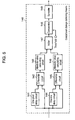
- Fig. 1 is a circuit block diagram illustrating the structure of image correction device 100 of the exemplary embodiment of the present invention.
- movement detecting means 120 compares the signal to one-frame-before image signal and detects an area with big temporal gradational change (hereinafter referred to as a movement area).
- Movement boundary detecting means 130 detects the boundary area of the movement area.
- gradational change detecting means 140 compares the gradation of adjoining pixels and detects an image area with big spatial gradational change.
- Combination determining means 150 determines the area excluding the image area with big gradational change by the following procedure: NOT-circuit 151 calculates logical NOT of the output from gradational change detecting means 140; AND-circuit 152 receives the result from NOT-circuit 151 and calculates logical conjunction of the result and the boundary area of the movement area.
- the logical NOT of the output from gradational change detecting means 140 shows the image area with small spatial gradational change (hereinafter, flat area); therefore, the output of combination determining means 150 shows the boundary area of the movement area that belongs to the flat area.
- Movement signal modulating means 160 modulates the output of movement detecting means 120 (as will be described later), whereas, for other areas, movement signal modulating means 160 sends the output of movement detecting means 120 to image correcting means 170.
- Image correcting means 170 of the embodiment changes a correction method according to the output of movement signal modulating means 160 so as to properly correct the dynamic pseudo contour.
- Fig. 2 is a circuit block diagram of movement detecting means 120 of the image correction device of the embodiment.
- One-frame delay circuit 121 delays an incoming image signal by one frame.
- Differential circuit 122 calculates the difference between the image signal and the one-frame-delayed image signal.
- Absolute value calculating circuit 123 calculates the absolute value of the difference.
- Comparator 124 compares the output from absolute value calculating circuit 123 to a threshold used for determining movement areas. If the output from absolute value calculating circuit 123 is greater than the threshold, comparator 124 outputs 1; otherwise, outputs 0.
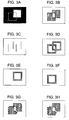
- Fig. 3 illustrates the workings of the image correction device of the present invention.
- Fig. 3A where, the rectangular shown by dot lines indicates the one-frame-before position of the pattern
- comparator 124 outputs movement area signals, as shown in Fig. 3B, according to the image signal: 1 for the movement area, 0 for other areas.
- Fig. 4 is a circuit block diagram of movement boundary detecting means 130 of the image correction device of the embodiment.
- One-pixel delay circuit 131 delays an incoming movement area signal by one pixel.
- Differential circuit 132 calculates the difference between the original movement area signal and the one-pixel-delayed movement area signal.
- Absolute value calculating circuit 133 calculates the absolute value of the difference. That is, absolute value calculating circuit 133 outputs a signal representing the horizontal boundaries of the movement area, as shown in Fig. 3C.
- one-line delay circuit 134 delays the movement area signal by one line.
- Differential circuit 135 calculates the difference between the original movement area signal and the one-line-delayed movement area signal.
- Absolute value calculating circuit 136 calculates the absolute value of the difference.
- absolute value calculating circuit 136 outputs a signal representing the vertical boundaries of the movement area.
- Adder 137 adds the outputs from absolute value calculating circuits 133 and 136.
- Comparator 138 compares the outputs from adder 137 to a threshold used for determining boundaries. If the output from adder 137 is greater than the threshold, comparator 138 outputs 1; otherwise, outputs 0.
- spreader 139 gives 1 to adjacent pixels, thereby increasing the area having 1.
- the area having 1 is extended horizontally by five pixels, and vertically by three pixels.
- Comparator 138 outputs 1 with respect to the horizontal 5 pixels and vertical 3 pixels around the boundary of the movement area, and outputs 0 with respect to other areas, so that the boundary area is extended, as shown in Fig. 3D.
- Fig. 5 is a circuit block diagram of gradational change detecting means 140 of the embodiment.
- Gradational change detecting means 140 contains one-pixel delay circuit 141; differential circuit 142; absolute value calculating circuit 143; one-line delay circuit 144; differential circuit 145; absolute value calculating circuit 146; adder 147; comparator 148; and spreader 149.
- the structure above is exactly alike to that of movement boundary detecting means 130, except that gradational change detecting means 140 receives an image signal as input signal.
- Comparator 148 outputs a gradational change signal showing the area with big gradational change, i.e., the boundary of the rectangular pattern of Fig. 3A. Therefore, as shown in Fig.
- comparator 148 outputs 1 with respect to the boundary of the rectangular pattern, and outputs 0 with respect to other areas.
- spreader 149 gives 1 to horizontal 5 pixels and vertical 3 pixels, thereby increasing the area having 1.
- Combination determining means 150 contains, as shown in Fig. 1, NOT-circuit 151 and AND-circuit 152.
- NOT-circuit 151 calculates logical NOT of a boundary change signal.
- Receiving the result from NOT-circuit 151, AND-circuit 152 calculates logical conjunction of the result and a movement boundary signal.
- the modulation control signal fed from combination determining means 150 gives 1 with respect to the boundary area of the movement area belongs to the flat area, and gives 0 with respect to other areas.
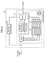
- Fig. 6 is a circuit block diagram of movement signal modulating means 160 of the image correction device.
- Movement signal modulating means 160 modulates a movement area signal so as to provide a movement area with parallel movement in the horizontal and vertical directions.
- Movement signal modulating means 160 contains four one-pixel delay circuits 161 1 - 161 4 , which sequentially delay a movement area signal by one pixel.
- selector 162 selects one signal from the original movement area signal and four delayed movement area signals.
- Random-number generator 163 generates a random number for each pixel; and accordingly, selector 162 outputs at latest 4-pixel-delayed movement area signal.
- selector 162 is now fed into selector 165 and one line-delayed circuits 164 1 , 164 2 .
- Selector 165 selects, according to the output from random number-generator 166, one signal, which provides the boundary of the movement area with a random diffusion in a vertical direction.
- selector 167 selects the horizontally and vertically modulated movement area signal; on the other hand, when the modulation control signal takes 0, selector 167 selects a movement area signal with no modulation.
- the selected signal is fed into image correcting means 170.
- the output from movement signal modulating means 160 provides the boundary of a movement area with a selective diffusion.
- the output signal is fed into image correcting means 170 as a correction control signal.
- the movement signal modulating means can be formed of a relatively simple structure.
- using the randomly selected amount of a delay of the delay circuits enables to provide the movement area with a diffusion having no periodical component, thereby further suppressing the switch shock.
- the amount of a delay may be periodically changed by pixel, line, or field, as long as the switch shock is not recognized as an eyesore.
- Fig. 7 is a circuit block diagram embodying image correcting means 170 of the image correction device of Fig. 1.
- Image correcting means 170 functions as a means for correcting dynamic pseudo contour and the structure thereof is the same as that of image correcting means 170 of the conventional device shown in Fig. 8. Therefore, the circuit blocks identical to those of image correcting means 170 bear similar reference numbers and detailed explanation thereof will be omitted.
- selector 7 selects the output from still-picture coding circuit 4
- the correction device provides image correction capable of showing a smooth gradation although dynamic pseudo contour easily appears; on the other hand, when selector 7 selects the output from motion-picture coding circuit 5, the correction device provides image correction for suppressing the dynamic pseudo contour although the number of the gradation levels decreases.
- Fig. 3D shows the boundary at which correction control is switched.
- the area shown in Fig. 3F of the entire boundary of Fig. 3D is the boundary between the rectangular pattern and the background in the one-frame-before image, but in the current frame, it belongs to a flat area with small gradational change. That is, as described earlier, the boundary area is supposed to suffer the switch shock.
- the correction control signal shown in Fig. 3H is used for operating selector 7, and correction control suitable for each area is selected.
- the correction control is switched at the boundary, whereas in the flat area susceptible to the switch shock, the boundary of correction undergoes selective diffusion.
- the switch shock is preferably suppressed and sufficient correction of dynamic pseudo contour is performed.
- the image correction method of the embodiment differs from the method that simply switches the image correction at the boundary of the movement area, and also differs from the method that provides the boundary area with a uniform diffusion.
- the method of the present invention provides the boundary area in a flat area-where the switch shock is likely to occur-with selective diffusion. In this way, the correction method of the embodiment not only can properly perform the image signal process according to the movement of images, but also suppresses the switch shock.
- movement signal modulating means 160 of the embodiment employs, as shown in Fig. 6, four one-pixel-delay circuits and two one-line-delay circuits, it is not limited thereto; the number of each delay circuit can be arbitrarily defined.
- spreaders 139 and 149 are disposed in the output-side of comparators 138 and 148, respectively. Receiving the output signal from comparator 138, spreader 139 extends the width of the boundary area corresponding to the signal in a horizontal direction; similarly, spreader 149 extends the width of the boundary area corresponding to the signal from comparator 148 in a vertical direction. However, it is not limited to the structure above as long as the width of the boundary area can be extended. For example, disposing a low pass filter in the input-side of a comparator can provide the same effect.
- image correcting means 170 of the embodiment is used for correcting dynamic pseudo contour in the description, it is not limited thereto.
- IP interlace-progressive
- the image correction device of the embodiment is applicable to other image corrections as long as the device contains an image correcting means capable of changing the correction process according to a control signal that corresponds to movement of images.
- the present invention can thus provide a method and device for image correction in which image signal processes are performed according to the movement of images, with occurrence of the switch shock preferably suppressed.
- the image signal process is performed according to the movement of images, with occurrence of the switch shock preferably suppressed.
- the device of the invention is therefore useful as the method and device for image correction that perform the image signal process according to movement of images.
Landscapes
- Engineering & Computer Science (AREA)
- Multimedia (AREA)
- Theoretical Computer Science (AREA)
- Signal Processing (AREA)
- Physics & Mathematics (AREA)
- General Physics & Mathematics (AREA)
- Computer Vision & Pattern Recognition (AREA)
- Computer Hardware Design (AREA)
- Picture Signal Circuits (AREA)
- Compression Or Coding Systems Of Tv Signals (AREA)
- Controls And Circuits For Display Device (AREA)
- Image Processing (AREA)
- Control Of Gas Discharge Display Tubes (AREA)
Abstract
Description
Claims (4)
- An image correction method that provides an image signal with image correction by switching correcting methods according to the image signal, the image correction method comprising:wherein, the image correction is performed differently between the image area having movement of which the boundary area is diffused and other areas.detecting an image area having movement according to the image signal;comparing gradation of image signals corresponding to adjoining pixels; andproviding a boundary area of the image area having movement with a diffusion process in an area having gradational change smaller than a predetermined threshold,
- An image correction device having a movement detecting means for detecting an image area having movement according to an image signal; and an image correcting means capable of providing the image signal with image correction and switching correction methods according to a control signal, the device further including:wherein, the image correcting means switches correction methods according to an output from the movement signal modulating means.a movement boundary detecting means for detecting a boundary area of the image area having movement;a gradational change detecting means for detecting an image area with great gradational change by comparing gradation of image signals corresponding to adjoining pixels; anda movement signal modulating means for providing the boundary area of the image area having movement with a diffusion process in an area excluding the image area with great gradational change,
- The image correction device of Claim 2, wherein the movement signal modulating means is formed of a delay circuit that delays an output of the movement detecting means at least in a horizontal direction or in a vertical direction.
- The image correction device of Claim 3, wherein the movement signal modulating means provides the boundary area of the image area having movement with a diffusion process by randomly switching an amount of delay fed from the delay circuit that delays the output of the movement detecting means in a horizontal direction or in a vertical direction.
Applications Claiming Priority (3)
| Application Number | Priority Date | Filing Date | Title |
|---|---|---|---|
| JP2004041108 | 2004-02-18 | ||
| JP2004041108 | 2004-02-18 | ||
| PCT/JP2005/002943 WO2005079059A1 (en) | 2004-02-18 | 2005-02-17 | Image correction method and image correction apparatus |
Publications (2)
| Publication Number | Publication Date |
|---|---|
| EP1599033A1 true EP1599033A1 (en) | 2005-11-23 |
| EP1599033A4 EP1599033A4 (en) | 2008-02-13 |
Family
ID=34857914
Family Applications (1)
| Application Number | Title | Priority Date | Filing Date |
|---|---|---|---|
| EP05710595A Withdrawn EP1599033A4 (en) | 2004-02-18 | 2005-02-17 | IMAGE CORRECTION METHOD AND IMAGE CORRECTION APPARATUS |
Country Status (5)
| Country | Link |
|---|---|
| US (1) | US7418152B2 (en) |
| EP (1) | EP1599033A4 (en) |
| KR (1) | KR100726142B1 (en) |
| CN (1) | CN100450147C (en) |
| WO (1) | WO2005079059A1 (en) |
Cited By (2)
| Publication number | Priority date | Publication date | Assignee | Title |
|---|---|---|---|---|
| EP1956830A4 (en) * | 2005-11-29 | 2010-09-29 | Panasonic Corp | REPRODUCTION DEVICE |
| CN102157135A (en) * | 2010-01-25 | 2011-08-17 | 精工爱普生株式会社 | Video processing circuit, video processing method, liquid crystal display device, and electronic apparatus |
Families Citing this family (29)
| Publication number | Priority date | Publication date | Assignee | Title |
|---|---|---|---|---|
| US7869662B2 (en) * | 2005-04-22 | 2011-01-11 | Agilent Technologies, Inc. | System architecture for sensing an absolute position using a target pattern |
| EP1936589A1 (en) * | 2006-12-20 | 2008-06-25 | Deutsche Thomson-Brandt Gmbh | Method and appartus for processing video pictures |
| EP1936590B1 (en) * | 2006-12-20 | 2016-07-20 | Thomson Licensing | Method and apparatus for processing video pictures |
| JP4245045B2 (en) * | 2006-12-26 | 2009-03-25 | ソニー株式会社 | Imaging apparatus, imaging signal processing method, and program |
| US12260023B2 (en) | 2012-01-17 | 2025-03-25 | Ultrahaptics IP Two Limited | Systems and methods for machine control |
| US8638989B2 (en) | 2012-01-17 | 2014-01-28 | Leap Motion, Inc. | Systems and methods for capturing motion in three-dimensional space |
| US9501152B2 (en) | 2013-01-15 | 2016-11-22 | Leap Motion, Inc. | Free-space user interface and control using virtual constructs |
| US10691219B2 (en) | 2012-01-17 | 2020-06-23 | Ultrahaptics IP Two Limited | Systems and methods for machine control |
| US11493998B2 (en) | 2012-01-17 | 2022-11-08 | Ultrahaptics IP Two Limited | Systems and methods for machine control |
| US8693731B2 (en) * | 2012-01-17 | 2014-04-08 | Leap Motion, Inc. | Enhanced contrast for object detection and characterization by optical imaging |
| US9679215B2 (en) | 2012-01-17 | 2017-06-13 | Leap Motion, Inc. | Systems and methods for machine control |
| US9070019B2 (en) | 2012-01-17 | 2015-06-30 | Leap Motion, Inc. | Systems and methods for capturing motion in three-dimensional space |
| US9459697B2 (en) | 2013-01-15 | 2016-10-04 | Leap Motion, Inc. | Dynamic, free-space user interactions for machine control |
| WO2014200589A2 (en) | 2013-03-15 | 2014-12-18 | Leap Motion, Inc. | Determining positional information for an object in space |
| US9916009B2 (en) | 2013-04-26 | 2018-03-13 | Leap Motion, Inc. | Non-tactile interface systems and methods |
| US10281987B1 (en) | 2013-08-09 | 2019-05-07 | Leap Motion, Inc. | Systems and methods of free-space gestural interaction |
| US10846942B1 (en) | 2013-08-29 | 2020-11-24 | Ultrahaptics IP Two Limited | Predictive information for free space gesture control and communication |
| US9632572B2 (en) | 2013-10-03 | 2017-04-25 | Leap Motion, Inc. | Enhanced field of view to augment three-dimensional (3D) sensory space for free-space gesture interpretation |
| US9996638B1 (en) | 2013-10-31 | 2018-06-12 | Leap Motion, Inc. | Predictive information for free space gesture control and communication |
| US9679197B1 (en) | 2014-03-13 | 2017-06-13 | Leap Motion, Inc. | Biometric aware object detection and tracking |
| US9785247B1 (en) | 2014-05-14 | 2017-10-10 | Leap Motion, Inc. | Systems and methods of tracking moving hands and recognizing gestural interactions |
| US9741169B1 (en) | 2014-05-20 | 2017-08-22 | Leap Motion, Inc. | Wearable augmented reality devices with object detection and tracking |
| CN204480228U (en) | 2014-08-08 | 2015-07-15 | 厉动公司 | motion sensing and imaging device |
| US10656720B1 (en) | 2015-01-16 | 2020-05-19 | Ultrahaptics IP Two Limited | Mode switching for integrated gestural interaction and multi-user collaboration in immersive virtual reality environments |
| EP3396413A4 (en) | 2015-12-21 | 2019-08-21 | Koito Manufacturing Co., Ltd. | Image acquisition device for vehicles, control device, vehicle provided with image acquisition device for vehicles and control device, and image acquisition method for vehicles |
| EP3396410A4 (en) | 2015-12-21 | 2019-08-21 | Koito Manufacturing Co., Ltd. | Image acquisition device for vehicles, control device, vehicle provided with image acquisition device for vehicles and control device, and image acquisition method for vehicles |
| JP6766071B2 (en) | 2015-12-21 | 2020-10-07 | 株式会社小糸製作所 | Image acquisition device for vehicles and vehicles equipped with it |
| EP3396414A4 (en) | 2015-12-21 | 2019-08-21 | Koito Manufacturing Co., Ltd. | IMAGE ACQUISITION DEVICE FOR USE BY A VEHICLE, CONTROL DEVICE, VEHICLE EQUIPPED WITH CONTROL DEVICE OR IMAGE ACQUISITION DEVICE FOR USE BY A VEHICLE, AND IMAGE ACQUISITION METHOD FOR USE BY A VEHICLE VEHICLE |
| CN117434008B (en) * | 2023-12-21 | 2024-07-02 | 海南中南标质量科学研究院有限公司 | Spectrum monitoring system and method based on artificial intelligence |
Family Cites Families (21)
| Publication number | Priority date | Publication date | Assignee | Title |
|---|---|---|---|---|
| JP3322809B2 (en) * | 1995-10-24 | 2002-09-09 | 富士通株式会社 | Display driving method and apparatus |
| WO1998044479A1 (en) * | 1997-03-31 | 1998-10-08 | Matsushita Electric Industrial Co., Ltd. | Dynamic image display method and device therefor |
| JP3758294B2 (en) * | 1997-04-10 | 2006-03-22 | 株式会社富士通ゼネラル | Moving picture correction method and moving picture correction circuit for display device |
| JP2994631B2 (en) * | 1997-12-10 | 1999-12-27 | 松下電器産業株式会社 | Drive pulse control device for PDP display |
| JP2994633B2 (en) * | 1997-12-10 | 1999-12-27 | 松下電器産業株式会社 | Pseudo-contour noise detection device and display device using the same |
| KR100370704B1 (en) * | 1998-04-17 | 2003-02-05 | 마쯔시다덴기산교 가부시키가이샤 | False contour correcting apparatus and method |
| US6496194B1 (en) * | 1998-07-30 | 2002-12-17 | Fujitsu Limited | Halftone display method and display apparatus for reducing halftone disturbances occurring in moving image portions |
| KR100488839B1 (en) * | 1999-01-22 | 2005-05-11 | 마츠시타 덴끼 산교 가부시키가이샤 | Apparatus and method for making a gray scale display with subframes |
| JP3457251B2 (en) | 1999-04-12 | 2003-10-14 | 松下電器産業株式会社 | Image display device |
| KR100734455B1 (en) * | 1999-04-12 | 2007-07-03 | 마츠시타 덴끼 산교 가부시키가이샤 | Image display apparatus |
| JP4519251B2 (en) * | 1999-10-13 | 2010-08-04 | シャープ株式会社 | Liquid crystal display device and control method thereof |
| US7068852B2 (en) * | 2001-01-23 | 2006-06-27 | Zoran Corporation | Edge detection and sharpening process for an image |
| JP3747317B2 (en) * | 2001-09-07 | 2006-02-22 | パイオニア株式会社 | Method for identifying moving image false contour occurrence location, image signal processing method, and image signal processing apparatus |
| US7433089B2 (en) * | 2001-09-27 | 2008-10-07 | Fujifilm Corporation | Image processor |
| KR100467447B1 (en) * | 2001-11-12 | 2005-01-24 | 삼성에스디아이 주식회사 | A method for displaying pictures on plasma display panel and an apparatus thereof |
| JP3879694B2 (en) | 2002-04-24 | 2007-02-14 | 松下電器産業株式会社 | Image display device |
| KR100486715B1 (en) * | 2002-10-09 | 2005-05-03 | 삼성전자주식회사 | Method and Apparatus for Reduction of False Contour in Digital Display Panel using Pulse Number Modulation |
| EP1434425A3 (en) * | 2002-12-25 | 2006-04-26 | Hitachi Ltd. | Video signal processing apparatus |
| JP4649108B2 (en) * | 2003-01-16 | 2011-03-09 | パナソニック株式会社 | Image display device and image display method |
| KR100496296B1 (en) * | 2003-02-08 | 2005-06-17 | 삼성에스디아이 주식회사 | Method and apparatus for displaying gray scale of plasma display panel |
| US7710358B2 (en) * | 2003-12-26 | 2010-05-04 | Panasonic Corporation | Image display apparatus for correcting dynamic false contours |
-
2005
- 2005-02-17 WO PCT/JP2005/002943 patent/WO2005079059A1/en not_active Ceased
- 2005-02-17 EP EP05710595A patent/EP1599033A4/en not_active Withdrawn
- 2005-02-17 US US10/542,026 patent/US7418152B2/en not_active Expired - Fee Related
- 2005-02-17 CN CNB2005800000509A patent/CN100450147C/en not_active Expired - Fee Related
- 2005-02-17 KR KR1020057020710A patent/KR100726142B1/en not_active Expired - Fee Related
Cited By (4)
| Publication number | Priority date | Publication date | Assignee | Title |
|---|---|---|---|---|
| EP1956830A4 (en) * | 2005-11-29 | 2010-09-29 | Panasonic Corp | REPRODUCTION DEVICE |
| US8351756B2 (en) | 2005-11-29 | 2013-01-08 | Panasonic Corporation | Reproduction device |
| CN102157135A (en) * | 2010-01-25 | 2011-08-17 | 精工爱普生株式会社 | Video processing circuit, video processing method, liquid crystal display device, and electronic apparatus |
| CN102157135B (en) * | 2010-01-25 | 2013-01-23 | 精工爱普生株式会社 | Image processing circuit and processing method, liquid crystal display device, and electronic apparatus |
Also Published As
| Publication number | Publication date |
|---|---|
| US7418152B2 (en) | 2008-08-26 |
| EP1599033A4 (en) | 2008-02-13 |
| CN1765120A (en) | 2006-04-26 |
| KR100726142B1 (en) | 2007-06-13 |
| CN100450147C (en) | 2009-01-07 |
| WO2005079059A1 (en) | 2005-08-25 |
| US20060050979A1 (en) | 2006-03-09 |
| KR20060007414A (en) | 2006-01-24 |
Similar Documents
| Publication | Publication Date | Title |
|---|---|---|
| US7418152B2 (en) | Method and device of image correction | |
| KR100505663B1 (en) | Progressive scan method of the display by adaptive edge dependent interpolation | |
| US7769089B1 (en) | Method and system for reducing noise level in a video signal | |
| KR100272582B1 (en) | Scan converter | |
| WO2004002135A1 (en) | Motion detection device and noise reduction device using that | |
| JPH10126649A (en) | Flicker reduction circuit | |
| JPH0937214A (en) | Progressive scan conversion method and progressive scan conversion device | |
| EP1104970A1 (en) | Method and device for converting number of frames of image signals | |
| KR100914619B1 (en) | Spatio-temporal adaptive video de-interlacing | |
| JP2004265382A (en) | Motion detection apparatus and method | |
| JP4355577B2 (en) | Up-conversion by noise suppression diagonal direction correction | |
| JP2008158732A (en) | Image processing device | |
| KR20060047635A (en) | Film mode display determination method, motion compensation image processing method, film mode detector and motion compensator | |
| KR101123975B1 (en) | Image signal processing apparatus | |
| KR20070098540A (en) | Recursive 3D ultra-precision method for slowly changing parts | |
| CN101630488B (en) | Self-adaptive video image dithering method for digital display system and device thereof | |
| KR101140442B1 (en) | Image status information correction | |
| JP2005267622A (en) | Image correction method and image correction apparatus | |
| JP2016142783A (en) | Display device | |
| US20070171301A1 (en) | Image static area determination apparatus and interlace progressive image transform apparatus | |
| KR101577703B1 (en) | Video picture display method to reduce the effects of blurring and double contours and device implementing this method | |
| JP2005311575A (en) | Frame cyclic noise reduction method | |
| JP4791275B2 (en) | Moving image noise removal device | |
| KR100606740B1 (en) | How to adjust the dynamic contrast | |
| JP5154208B2 (en) | Image signal processing device |
Legal Events
| Date | Code | Title | Description |
|---|---|---|---|
| PUAI | Public reference made under article 153(3) epc to a published international application that has entered the european phase |
Free format text: ORIGINAL CODE: 0009012 |
|
| 17P | Request for examination filed |
Effective date: 20050627 |
|
| AK | Designated contracting states |
Kind code of ref document: A1 Designated state(s): AT BE BG CH CY CZ DE DK EE ES FI FR GB GR HU IE IS IT LI LT LU MC NL PL PT RO SE SI SK TR |
|
| AX | Request for extension of the european patent |
Extension state: AL BA HR LV MK YU |
|
| DAX | Request for extension of the european patent (deleted) | ||
| RBV | Designated contracting states (corrected) |
Designated state(s): DE FR GB NL |
|
| A4 | Supplementary search report drawn up and despatched |
Effective date: 20080116 |
|
| RIC1 | Information provided on ipc code assigned before grant |
Ipc: H04N 5/21 20060101ALI20080110BHEP Ipc: H04N 5/20 20060101AFI20050831BHEP |
|
| RAP1 | Party data changed (applicant data changed or rights of an application transferred) |
Owner name: PANASONIC CORPORATION |
|
| 17Q | First examination report despatched |
Effective date: 20120206 |
|
| STAA | Information on the status of an ep patent application or granted ep patent |
Free format text: STATUS: THE APPLICATION IS DEEMED TO BE WITHDRAWN |
|
| 18D | Application deemed to be withdrawn |
Effective date: 20120417 |