EP1598663A2 - Method and apparatus for X-ray analysis with a two-dimensional array-detector - Google Patents
Method and apparatus for X-ray analysis with a two-dimensional array-detector Download PDFInfo
- Publication number
- EP1598663A2 EP1598663A2 EP05009958A EP05009958A EP1598663A2 EP 1598663 A2 EP1598663 A2 EP 1598663A2 EP 05009958 A EP05009958 A EP 05009958A EP 05009958 A EP05009958 A EP 05009958A EP 1598663 A2 EP1598663 A2 EP 1598663A2
- Authority
- EP
- European Patent Office
- Prior art keywords
- detector
- data set
- pixel
- source
- data sets
- Prior art date
- Legal status (The legal status is an assumption and is not a legal conclusion. Google has not performed a legal analysis and makes no representation as to the accuracy of the status listed.)
- Granted
Links
- 238000000034 method Methods 0.000 title claims abstract description 45
- 238000002441 X-ray diffraction Methods 0.000 title claims abstract description 29
- 230000002950 deficient Effects 0.000 claims description 18
- 238000006073 displacement reaction Methods 0.000 claims description 16
- 238000005259 measurement Methods 0.000 claims description 11
- 230000035945 sensitivity Effects 0.000 claims description 7
- 238000009826 distribution Methods 0.000 claims description 6
- 238000001514 detection method Methods 0.000 claims description 5
- 238000001228 spectrum Methods 0.000 claims description 4
- 239000004020 conductor Substances 0.000 claims description 2
- 230000000737 periodic effect Effects 0.000 claims description 2
- 229920001721 polyimide Polymers 0.000 claims description 2
- 230000008054 signal transmission Effects 0.000 claims description 2
- 239000010409 thin film Substances 0.000 claims description 2
- 230000008569 process Effects 0.000 abstract description 2
- 238000011156 evaluation Methods 0.000 description 7
- 230000000694 effects Effects 0.000 description 6
- 230000005855 radiation Effects 0.000 description 5
- 230000003287 optical effect Effects 0.000 description 4
- 238000011161 development Methods 0.000 description 3
- 238000004519 manufacturing process Methods 0.000 description 3
- 238000005457 optimization Methods 0.000 description 3
- 230000009467 reduction Effects 0.000 description 3
- 239000004065 semiconductor Substances 0.000 description 3
- 208000012886 Vertigo Diseases 0.000 description 2
- 239000002131 composite material Substances 0.000 description 2
- 238000003384 imaging method Methods 0.000 description 2
- 230000006872 improvement Effects 0.000 description 2
- 229910004613 CdTe Inorganic materials 0.000 description 1
- 229910001218 Gallium arsenide Inorganic materials 0.000 description 1
- 241000220317 Rosa Species 0.000 description 1
- 238000003491 array Methods 0.000 description 1
- 238000004364 calculation method Methods 0.000 description 1
- 230000008859 change Effects 0.000 description 1
- 238000010276 construction Methods 0.000 description 1
- 238000013461 design Methods 0.000 description 1
- 238000005516 engineering process Methods 0.000 description 1
- 230000036541 health Effects 0.000 description 1
- 239000000463 material Substances 0.000 description 1
- 230000005433 particle physics related processes and functions Effects 0.000 description 1
- 230000002093 peripheral effect Effects 0.000 description 1
- 238000012545 processing Methods 0.000 description 1
- 238000011160 research Methods 0.000 description 1
Images


Classifications
-
- G—PHYSICS
- G01—MEASURING; TESTING
- G01N—INVESTIGATING OR ANALYSING MATERIALS BY DETERMINING THEIR CHEMICAL OR PHYSICAL PROPERTIES
- G01N23/00—Investigating or analysing materials by the use of wave or particle radiation, e.g. X-rays or neutrons, not covered by groups G01N3/00 – G01N17/00, G01N21/00 or G01N22/00
- G01N23/20—Investigating or analysing materials by the use of wave or particle radiation, e.g. X-rays or neutrons, not covered by groups G01N3/00 – G01N17/00, G01N21/00 or G01N22/00 by using diffraction of the radiation by the materials, e.g. for investigating crystal structure; by using scattering of the radiation by the materials, e.g. for investigating non-crystalline materials; by using reflection of the radiation by the materials
- G01N23/207—Diffractometry using detectors, e.g. using a probe in a central position and one or more displaceable detectors in circumferential positions
Definitions
- the invention relates to a method for operating an X-ray analysis device with a source of x-radiation, an object to be examined, which coincides with the X-ray is illuminated, and a two-dimensional planar array detector with pixel elements for spatially resolved detection of the object outgoing X-rays, creating a record, especially in shape a digitized diffractogram and / or spectrum is obtained.
- the invention relates to an X-ray analysis apparatus for performing the Process.
- Two-dimensional array detectors used in X-ray analyzers of the above mentioned type are among others from Gerhard Lutz "Semiconductor radiation detectors ", B. Mikulec et al.” Development of Segmented Semiconductor Arrays for Quantum Imaging "Elsevier Science, N. Wermes” Pixel detectors for particle physics and imaging applications "Elsevier Science Direct and Edwin M. Westbrook's National Institute of Health grant application www.brunel.ac.uk/research/rose/3D/publications.html known. Such an array Detectors consist of a large number of photosensitive pixel elements, which in Form of an array are arranged on a chip.
- the sensor chip is for usually by bump bonding with an ASIC (Application Specific Circuit) which includes electronic channels, amplifiers and discriminators.
- ASIC Application Specific Circuit
- the photosensitive pixel elements are fixedly connected to the ASIC and a Replacing a defective pixel element is not possible, make erroneous, especially blind pixel elements is a big technical problem. It will while trying to figure out the number of blind pixel elements To reduce manufacturing improvement, due to the great complexity of However, hybrid production (sensor, bump bonds, highly integrated ASIC) will be hampered For the foreseeable future, only very expensive 100% functioning pixel detectors will be available. For therefore, one usually takes the presence of isolated blind people Pixel elements and the resulting missing information in the corresponding areas in purchase.
- one-dimensional detectors are known (H. Göbel, Adv. In X-Ray Analysis 22 (1978) 255-265), which are moved by means of a goniometer by changing the 20 value over the range of interest for the measurement so that certain ranges can be detected by different pixels. With this method, however, only one-dimensional recordings are possible. Furthermore, in such an arrangement, the optics for focusing the radiation on the detector must be moved with the detector, which requires a complex and particularly stable construction of the structure.
- Object of the present invention is therefore to provide a method for operating a X-ray analysis device with a two-dimensional array detector with pixel elements to propose that, despite the presence of blind pixel elements in the detector to reduce the number of dead pixels in the record or to avoid and as complete a record as possible to obtain. Furthermore, an X-ray analysis device is to be proposed, with which this method can be carried out.
- Step d) the steps b) to c) with varying displacement once or several times repeated. This allows the number of dead pixels in the record to be arbitrary be reduced.
- a development of this variant provides that the data records during a continuous, preferably periodic displacement and / or rotation of the Detector be recorded.
- the total data set then includes the integrated data between two positions of the detector.
- the detector therefore becomes between two shots of consecutive records by exactly one Moved pixel element.
- a further object of the invention is a method for operating an X-ray analysis device to propose that the measurement of a record with a Resolution greater than the dimensions of each pixel element.
- a further variant of the method according to the invention therefore provides that the detector is shifted by a fraction, preferably 1 / n, of a pixel element between two recordings of successive data records, where n ⁇ N, preferably n ⁇ 10 Detector to a subpixel, the spatial resolution can be increased. This is particularly advantageous for detectors with large pixel elements or for the recording of very small structures. The resolution of the detector is thereby improved so that structures within a pixel element can be detected. In order to obtain a uniform resolution over the entire detector range, n shifts must be carried out with the corresponding recordings.
- the displacements of the Detector different directions in the detector surface.
- the postponement of the detector can then be done within the entire area of the detector, so that optimization with respect to the position of the dead pixels is simplified.
- step d) the pixels of the border areas of the entire record, which does not include the records of all individual recordings weighted according to the inverse of their admission frequency become. For each pixel then results in a mean signal intensity.
- Each pixel element is individually a sensitivity and / or a statistical Associated error and / or offset for the recorded reading, in step d) in a weighting of the respective pixel in the overlay taken into account.
- the shots of the individual Data sets are thus not affected by the varying sensitivity and / or falsified the statistical error or offset.
- the superimposition of the recorded individual data sets is preferably carried out such that for each of the data points to be overlaid the offset is subtracted, the measured value according to the sensitivity of the respective pixel element normalized and inversely weighted to the size of the associated statistical error where the overall weighting for each pixel is 1 or 100%.
- the contributions are individual Pixel elements in the overlay of the data records in step d) fixed with 0 weighted, especially with defective pixel elements, which are known that they are blind, generate strongly fluctuating signals or constantly their saturation value Show. Due to the strong distorting effects of such Pixel elements, it seems advantageous to weight these with 0 and the values of the corresponding pixels for the entire data set from the remaining data sets to win.
- each pixel must be at least once taken by a non-0 pixel element. It is therefore advantageous, the trajectories of the respective shifts to the spatial Adjust the distribution of defective pixel elements, especially such that as far as possible no data point of the entire data set exclusively the superposition of signal contributions of defective pixel elements.
- the detector several each over blind border areas adjacent to each other Sensor chips is composed, and that the blind edge areas like damaged pixel elements are treated.
- such composite detectors have many non-photosensitive areas is it is possible by the inventive method, total data sets which does not have holes due to the lack of active pixel elements have the corresponding edge regions of the sensor chips.
- the trajectories of the respective shifts are chosen that the overall statistical error of the entire data set is minimized. On This way, dead pixels or 0 weighted pixels on as possible distributed many different positions and avoided double-blind measurements become.
- the X-ray analysis apparatus is for carrying out the previously described Set up procedure.
- An advantageous embodiment of the X-ray analysis device provides a piezo drive to move the detector.
- a piezo drive Shifts on ⁇ m scale and below are realizable, so that almost Any shifts of the detector are possible.
- a further embodiment of the X-ray analysis device provides that the Array detector along with a first stage of evaluation electronics a carrier which is not moved during the measurement is movably arranged, the first stage via a flexible connection with another stage of the Evaluation electronics for signal transmission is electrically connected. To this Way, a fast preamplifier can be attached very close to the detector, resulting in an improvement of the signal-to-noise ratio. The flexible connection of the first stage with another stage of the evaluation electronics the mobility of the detector is ensured.
- a development of the X-ray analysis device according to the invention provides that the flexible connection a thin film, preferably a polyimide film with integrated Includes printed conductors.
- the width B of the blind edge regions is an integer multiple of Width b of a pixel element. Due to the non-sensitive edge areas in the first single data record missing data points can then by a shift of the detector to obtain an integer number of pixel elements become.
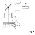
- Fig. 1 shows schematically the essential elements of an X-ray analysis device.
- the X-radiation emitted by a source 17 is modified by means of optical elements 18 and exposes an object 19 of special X-radiation.
- the X-ray beam is focused onto the detector by means of optical elements 18.
- the array detector is equipped with an X-ray sensitive single detector 1 , a first stage 2 of an evaluation (ASIC), a carrier 3 and a piezo drive 4 , wherein the single detector 1 is contacted by bumps 5 with the first stage 2 of the transmitter and firmly connected.
- ASIC evaluation
- the connection between the single detector 1 and the carrier 3 is realized by means of a flexible connection 6 , which includes electrical connections from the first stage 2 of the transmitter to a further stage of the transmitter, which may be located, for example, on the carrier 3.
- a flexible connection 6 which includes electrical connections from the first stage 2 of the transmitter to a further stage of the transmitter, which may be located, for example, on the carrier 3.
- the mass of the components to be moved is kept low, so that the shift can be done quickly and easily by using a piezoelectric drive 4, on the other hand, by the Mitverschieben the first stage 2 of the evaluation a low noise preamplification and first digital processing of the detected signals take place and thus a good signal / noise ratio can be achieved.
- the displacement of the single detector 1 takes place in one or in two dimensions such that the radial distance r of the single detector 1 to the object 19 does not change. The movement is indicated by the arrow. Thus, there is no need to focus on a new level.
- the single detector 1 of Fig. 1 is shown here in a planar design. However, it is also conceivable to provide curved embodiments.
- the X-ray sensitive pixel elements 7 (!!! is not marked in any drawing !!!) of the single detector 1 are typically made of Si or other semiconductor materials such as GaAs, CdTe, CZT.
- the transmitter 2 is typically implemented in CMOS or Bi-CMOS technology, eg in 0.35 ⁇ m feature sizes.
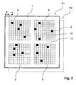
- FIG. 1 An overall detector 1 is shown in FIG . Since the individual sensor chips 8 , which are usually produced, are generally smaller than the desired single detector area, the single detector 1 is composed of a plurality of sensor chips 8. However, this has the consequence that, in addition to the defective pixel elements 9 contained in the sensor chips 8, edge regions 10 of the sensor chips 8 are additionally located within the individual detector area, from which information for the data record to be recorded can not be taken. Both the defective pixel elements 9 and the edge regions 10 of the sensor chips 8 therefore produce dead pixels 12 a, 12 b in a recorded data record 11 . In order to avoid distortions of information within a data set 11, defective pixel elements 9 in the data set are weighted with 0.
- blind pixel elements these also include pixel elements that generate strongly fluctuating signals or constantly reach their saturation value. Such pixel elements can be located by a 0-measurement.
- Common sensor chips include about 1,000 x 1,000 pixel elements. For the sake of simplicity, the sensor chips 8 shown in FIG. 2 have been shown with only 10 x 10 pixel elements.
- FIG. 3a shows a schematic representation of the distribution of dead pixels 12a, 12b in a data record 11, which was recorded by a single detector 1, as shown in FIG.
- the isolated dead pixels 12a which result from the defective pixel elements 9 of the single detector 1
- this is impractical if the radiation to be detected has to be focused on a specific plane, as is required, for example, in Bragg-Brentano geometry in X-ray diffractometry.
- the sensor chips 8 are therefore arranged in a plane.
- the single detector 1 is moved after a first recording of a first data set in a position P1 from this position P1 to a position P2, as shown in Fig. 2.
- a further data record 11 is recorded, which is superimposed with the first data record 11, so that a total data record 13 is formed.
- the width B of the blind edge regions of the sensor chips 8 in the method according to the invention is preferably an integer multiple of the width b of a pixel element, the width b of a pixel element moving in the order of 50 to 100 ⁇ m. In this way, it is possible to completely coincide a pixel element in position P1 with a pixel element in position P2 by shifting the single detector 1 by an integer multiple of a pixel element 7.
- Fig. 3b shows the distribution of the dead pixels 12 in the total data set 13, which is obtained from the data sets 11 of the measurements in the positions P1 and P2.
- the shift of the single detector 1 is chosen arbitrarily here and was 2x2 pixel elements. It can be seen from the overall data set 13 that the number of dead pixels 12 compared to the number of dead pixels 12a, 12b in the data set 11 of FIG. 3 is considerably reduced. With a suitable optimization of the displacement of the individual detector 1, a further reduction of the dead pixels 12 in the overall data set 13 can be achieved, ideally zero dead pixels 12. Likewise, the result by recording more records 11 in different positions of the single detector 1 and their superposition an overall data record 13 can be improved.
- the predetermined measurement time can be selected long enough for the recordings of the individual data records 11 to be made.
- XRD X-Ray Diffraction
- the different sensitivities of the individual pixel elements 7 become by a weighting of the individual pixels when superimposing the individual data sets considered.
- every pixel element can have a statistical error as well as an offset for the recorded measured value, which are stored in the Weighting of the respective pixel when superimposing the recorded data sets 11 be taken into account. This is for the data points to be overlaid in each case the offset is subtracted, the measured value according to the sensitivity of the respective pixel element 7 normalized and inversely to the size of the associated Statistical error is weighted, so for each pixel the overall weighting 1 or 100% results.
- sensor chips which have larger pixel elements in their edge regions (superpixel elements). These superpixel elements cause the resolution in these areas to be reduced. By means of the method according to the invention, this unpleasant effect can also be eliminated since, with a suitable displacement of the sensor chips 8, the areas which were previously measured by the superpixel elements are measured by a photosensitive pixel element 15 during at least one further measurement. This results in a more homogeneous spatial resolution over the entire detector surface.
- Fig. 4 this is shown schematically.
- a roughly structured rectangular single detector 8 is shifted diagonally to a position P2 (thin frame) around a sub-pixel element, in this case by half of a pixel element 7, after recording a first data set in a position P1 (bold frame). In this way, changes in the signal within a pixel can be detected, thereby increasing the spatial resolution of the entire data set.
- the advantages of the invention are particularly effective if one or several shifts by an integer multiple of a pixel element. 7 with one or more subsequent shifts by one subpixel be combined with each other. In this way one obtains using a conventional single detector 1 a total data set with a reduced number of dead pixels 12, ideally zero, and improved Spatial resolution.
- the application of the method according to the invention is not limited to rectangular sensor chips 8.
- Radially symmetrical sensor chips 14 with ring segments as pixel elements, as shown in FIG. 5 can also be used for this method.
- the displacement here takes place preferably in the form of a rotational movement about the midpoint of the radially symmetrical individual detector 14. For the calculation or optimization of the displacement, it makes sense to use polar coordinates in such radially symmetrical sensor chips.
- the defective or weighted with 0 pixel elements 9 are moved to adjacent squares 16 , so that the dead pixels of the first record in the second record by fotosenisitver pixel elements 15 are measured and thus constructively contribute to the overall data set.
- the X-ray analysis apparatus or the invention Method for operating an X-ray analyzer enabled simple way, in particular without displacement of the X-ray analyzer belonging to optical elements, a reduction of due to defective or dead pixels in the data set resulting from 0 weighted pixel elements.
- a reduction of due to defective or dead pixels in the data set resulting from 0 weighted pixel elements when using from multiple sensor chips composite single detector disturbing influences of the edge areas in the Creation of records are avoided.
Landscapes
- Chemical & Material Sciences (AREA)
- Crystallography & Structural Chemistry (AREA)
- Physics & Mathematics (AREA)
- Health & Medical Sciences (AREA)
- Life Sciences & Earth Sciences (AREA)
- Analytical Chemistry (AREA)
- Biochemistry (AREA)
- General Health & Medical Sciences (AREA)
- General Physics & Mathematics (AREA)
- Immunology (AREA)
- Pathology (AREA)
- Analysing Materials By The Use Of Radiation (AREA)
- Measurement Of Radiation (AREA)
Abstract
Description
Die Erfindung betrifft ein Verfahren zum Betrieb eines Röntgenanalysegerätes mit einer Quelle für Röntgenstrahlung, einem zu untersuchenden Objekt, das mit der Röntgenstrahlung beleuchtet wird, und einem flächigen zweidimensionalen Array-Detektor mit Pixel-Elementen zum ortsaufgelösten Nachweis der von dem Objekt ausgehenden Röntgenstrahlung, wodurch ein Datensatz, insbesondere in Form eines digitalisierten Diffraktogramms und/oder Spektrums erhalten wird. Des Weiteren betrifft die Erfindung ein Röntgenanalysegerät zum Durchführen des Verfahrens. The invention relates to a method for operating an X-ray analysis device with a source of x-radiation, an object to be examined, which coincides with the X-ray is illuminated, and a two-dimensional planar array detector with pixel elements for spatially resolved detection of the object outgoing X-rays, creating a record, especially in shape a digitized diffractogram and / or spectrum is obtained. Of Furthermore, the invention relates to an X-ray analysis apparatus for performing the Process.
Zweidimensionale Array-Detektoren, die in Röntgenanalysegeräten der oben genannten Art Verwendung finden sind unter Anderem aus Gerhard Lutz "Semiconductor radiation detectors", B. Mikulec et al. "Development of Segmented Semiconductor Arrays for Quantum Imaging" Elsevier Science, N. Wermes "Pixel detectors for particle physics and imaging applications" Elsevier Science Direct und Edwin M. Westbrook National Institute of Health Förderantrag www.brunel.ac.uk/research/rose/3D/publications.html bekannt. Derartige Array Detektoren bestehen aus einer Vielzahl an fotosensitiven Pixel-Elementen, die in Form eines Arrays auf einem Chip angeordnet sind. Der Sensor-Chip ist für gewöhnlich mittels Bump-Bonding mit einem ASIC (Application Specific Circuit) kontaktiert, der elektronische Kanäle, Verstärker und Diskriminatoren umfasst. Da die fotosensitiven Pixel-Elemente fest mit dem ASIC verbunden sind und ein Austausch eines fehlerhaften Pixel-Elements nicht möglich ist, stellen fehlerhafte, insbesondere blinde Pixel-Elemente ein großes technisches Problem dar. Es wird zwar versucht, die Anzahl der blinden Pixel-Elemente durch Fertigungsverbesserung zu reduzieren, aufgrund der großen Komplexität der Hybridfertigung (Sensor, Bump-Bonds, hochintegriertes ASIC) wird es jedoch auf absehbare Zeit nur sehr teure 100 % funktionierende Pixel-Detektoren geben. Für gewöhnlich nimmt man deshalb das Vorhandensein von vereinzelten blinden Pixel-Elementen und die dadurch auftretenden fehlenden Informationen in den entsprechenden Bereichen in Kauf.Two-dimensional array detectors used in X-ray analyzers of the above mentioned type are among others from Gerhard Lutz "Semiconductor radiation detectors ", B. Mikulec et al." Development of Segmented Semiconductor Arrays for Quantum Imaging "Elsevier Science, N. Wermes" Pixel detectors for particle physics and imaging applications "Elsevier Science Direct and Edwin M. Westbrook's National Institute of Health grant application www.brunel.ac.uk/research/rose/3D/publications.html known. Such an array Detectors consist of a large number of photosensitive pixel elements, which in Form of an array are arranged on a chip. The sensor chip is for usually by bump bonding with an ASIC (Application Specific Circuit) which includes electronic channels, amplifiers and discriminators. There the photosensitive pixel elements are fixedly connected to the ASIC and a Replacing a defective pixel element is not possible, make erroneous, especially blind pixel elements is a big technical problem. It will while trying to figure out the number of blind pixel elements To reduce manufacturing improvement, due to the great complexity of However, hybrid production (sensor, bump bonds, highly integrated ASIC) will be hampered For the foreseeable future, only very expensive 100% functioning pixel detectors will be available. For therefore, one usually takes the presence of isolated blind people Pixel elements and the resulting missing information in the corresponding areas in purchase.
Um den dadurch resultierenden störenden Effekt von beispielsweise schwarzen Bildbereichen (tote Pixel) zu vermeiden ist es bekannt, mehrere Pixel zu einem Superpixel zusammenzufassen. Durch dieses Verfahren wird jedoch die Auflösung der entsprechenden Aufnahmen verschlechtert. Möchte man Effekte beobachten, die in der Größenordnung eines Pixel-Elements liegen, können einzelne blinde Pixel-Elemente zu einer gravierenden Datenverfälschung führen, da möglicherweise genau die Bereiche der toten Pixel wichtige Informationen enthalten würden. To the resulting disturbing effect of, for example, black To avoid image areas (dead pixels) it is known to make several pixels into one To summarize super pixels. By this method, however, the Resolution of the corresponding pictures deteriorated. Do you want effects can observe, which are in the order of a pixel element individual blind pixel elements lead to serious data corruption, there may be just the areas of dead pixels important information would contain.
Neben zweidimensionalen Array-Detektoren sind eindimensionale Detektoren bekannt (H. Göbel, Adv. In X-Ray Analysis 22 (1978) 255-265), die mit Hilfe eines Goniometers durch Veränderung des 20-Wertes über den für die Messung interessanten Bereich verfahren werden können, so dass bestimmte Messbereiche von verschiedenen Pixeln erfasst werden können. Mit dieser Methode sind jedoch lediglich eindimensionale Aufnahmen möglich. Des Weiteren muss bei einer derartigen Anordnung die Optik zum Fokussieren der Strahlung auf den Detektor mit dem Detektor verfahren werden, was eine aufwändige und besonders stabile Konstruktion des Aufbaus erfordert.In addition to two-dimensional array detectors one-dimensional detectors are known (H. Göbel, Adv. In X-Ray Analysis 22 (1978) 255-265), which are moved by means of a goniometer by changing the 20 value over the range of interest for the measurement so that certain ranges can be detected by different pixels. With this method, however, only one-dimensional recordings are possible. Furthermore, in such an arrangement, the optics for focusing the radiation on the detector must be moved with the detector, which requires a complex and particularly stable construction of the structure.
Aufgabe der vorliegenden Erfindung ist es daher, ein Verfahren zum Betrieb eines Röntgenanalysegeräts mit einem zweidimensionalen Array-Detektor mit Pixel-Elementen vorzuschlagen, das es erlaubt, trotz des Vorhandenseins blinder Pixel-Elemente im Detektor, die Anzahl der toten Pixel im Datensatz zu reduzieren beziehungsweise zu vermeiden und so einen möglichst vollständigen Datensatz zu erhalten. Des Weiteren soll ein Röntgenanalysegerät vorgeschlagen werden, mit dem dieses Verfahren ausgeführt werden kann.Object of the present invention is therefore to provide a method for operating a X-ray analysis device with a two-dimensional array detector with pixel elements to propose that, despite the presence of blind pixel elements in the detector to reduce the number of dead pixels in the record or to avoid and as complete a record as possible to obtain. Furthermore, an X-ray analysis device is to be proposed, with which this method can be carried out.
Diese Aufgabe wird erfindungsgemäß durch ein Verfahren zum Betrieb eines
Röntgenanalysegeräts gelöst, das sich durch folgende Schritte auszeichnet:
Durch das Verschieben des Detektors zwischen den Aufnahmen zweier Datensätze verschieben sich schadhaften Pixel-Elemente relativ zu dem zu untersuchenden Objekt, so dass mit einer relativ hohen Wahrscheinlichkeit die vom Objekt ausgehende Strahlung, die bei der ersten Aufnahme auf schadhafte Pixel-Elemente getroffen ist, nach dem Verschieben bei der Aufnahme des zweiten Datensatzes auf ein fotosensitives Pixel-Element trifft. Durch die Überlagerung der beiden aufgenommenen Datensätze kann eine effizientere Detektion der Röntgenstrahlung erfolgen und die Anzahl toter Pixel im Gesamtdatensatz reduziert werden.By moving the detector between the recordings of two data sets move defective pixel elements relative to the one to be examined Object, so that with a relatively high probability that of the object outgoing radiation, the first time you take on defective pixel elements is taken, after moving when recording the second record encounters a photosensitive pixel element. Due to the superimposition of the Both recorded data records can be a more efficient detection of X-rays and reduces the number of dead pixels in the overall data set become.
Bei einer bevorzugten Variante des erfindungsgemäßen Verfahrens werden vor Schritt d) die Schritte b) bis c) mit variierender Verschiebung einmal oder mehrfach wiederholt. Hierdurch kann die Anzahl der toten Pixel im Datensatz beliebig reduziert werden.In a preferred variant of the method according to the invention are Step d) the steps b) to c) with varying displacement once or several times repeated. This allows the number of dead pixels in the record to be arbitrary be reduced.
Eine Weiterbildung dieser Variante sieht vor, dass die Datensätze während einer kontinuierlichen, vorzugsweise periodischen Verschiebung und/oder Drehung des Detektors aufgenommen werden. Der Gesamtdatensatz umfasst dann die aufintegrierten Daten zwischen zwei Positionen des Detektors.A development of this variant provides that the data records during a continuous, preferably periodic displacement and / or rotation of the Detector be recorded. The total data set then includes the integrated data between two positions of the detector.
Mit der Verschiebung und/oder Drehung des Detektors werden zwischen zwei Aufnahmen von Datensätzen vorzugsweise weniger als 10 Pixel überstrichen, so dass ein möglichst großer Überlapp der mehrfach vermessenen Bereiche realisiert wird.With the displacement and / or rotation of the detector are between two shots of records preferably swept less than 10 pixels, so that realizes the largest possible overlap of the multiply measured areas becomes.
In einer besonders bevorzugten Variante des Verfahrens wird der Detektor daher zwischen zwei Aufnahmen von aufeinander folgenden Datensätzen um genau ein Pixel-Element verschoben.In a particularly preferred variant of the method, the detector therefore becomes between two shots of consecutive records by exactly one Moved pixel element.
Eine weitere Aufgabe der Erfindung ist es, ein Verfahren zum Betrieb eines Röntgenanalysegeräts vorzuschlagen, das die Messung eines Datensatzes mit einer Auflösung erlaubt, die größer ist als die Ausmaße der einzelnen Pixel-Elemente. A further object of the invention is a method for operating an X-ray analysis device to propose that the measurement of a record with a Resolution greater than the dimensions of each pixel element.
Eine weitere Variante des erfindungsgemäßen Verfahrens sieht daher vor, dass zwischen zwei Aufnahmen von aufeinander folgenden Datensätzen der Detektor um einen Bruchteil, vorzugsweise 1 / n eines Pixel-Elements, verschoben wird, wobei n ∈ N , vorzugsweise n < 10. Durch diese Verschiebung des Detektors um ein Subpixel kann die Ortsauflösung erhöht werden. Dies ist insbesondere für Detektoren mit großen Pixel-Elementen vorteilhaft beziehungsweise für die Aufnahme sehr kleiner Strukturen. Die Auflösung des Detektors wird hierdurch derart verbessert, dass Strukturen innerhalb eines Pixel-Elements detektiert werden können. Um eine einheitliche Auflösung über den gesamten Detektor-Bereich zu bekommen, müssen n Verschiebungen mit den entsprechenden Aufnahmen durchgeführt werden.A further variant of the method according to the invention therefore provides that the detector is shifted by a fraction, preferably 1 / n, of a pixel element between two recordings of successive data records, where n ∈ N, preferably n <10 Detector to a subpixel, the spatial resolution can be increased. This is particularly advantageous for detectors with large pixel elements or for the recording of very small structures. The resolution of the detector is thereby improved so that structures within a pixel element can be detected. In order to obtain a uniform resolution over the entire detector range, n shifts must be carried out with the corresponding recordings.
In einer vorteilhaften Variante des Verfahrens umfassen die Verschiebungen des Detektors unterschiedliche Richtungen in der Detektor-Fläche. Die Verschiebung des Detektors kann dann innerhalb der ganzen Fläche des Detektors erfolgen, so dass eine Optimierung bezüglich der Lage der toten Pixel vereinfacht wird.In an advantageous variant of the method, the displacements of the Detector different directions in the detector surface. The postponement of the detector can then be done within the entire area of the detector, so that optimization with respect to the position of the dead pixels is simplified.
Da bei dem erfindungsgemäßen Verfahren einige Bereiche des Datensatzes, insbesondere die Randbereiche, weniger oft aufgenommen werden, als der zentrale Bereich des Datensatzes, ist es vorteilhaft, wenn in Schritt d) die Pixel der Randbereiche des gesamten Datensatzes, zu denen nicht die Datensätze aller Einzelaufnahmen beitragen, entsprechend dem Inversen ihrer Aufnahmehäufigkeit gewichtet werden. Für jedes Pixel ergibt sich dann eine mittlere Signalintensität.As in the inventive method some areas of the data set, in particular the peripheral areas are less often taken than the central one Area of the record, it is advantageous if in step d) the pixels of the border areas of the entire record, which does not include the records of all individual recordings weighted according to the inverse of their admission frequency become. For each pixel then results in a mean signal intensity.
In einer besonders bevorzugten Variante des erfindungsgemäßen Verfahrens werden jedem Pixel-Element individuell eine Empfindlichkeit und/oder ein statistischer Fehler und/oder ein Offset für den aufgenommenen Messwert zugeordnet, die in Schritt d) in einer Gewichtung des jeweiligen Pixels bei der Überlagerung der aufgenommenen Datensätze berücksichtigt werden. Die Aufnahmen der einzelnen Datensätze werden somit nicht durch die variierende Empfindlichkeit und/oder den statistischen Fehler beziehungsweise durch einen Offset verfälscht. In a particularly preferred variant of the method according to the invention Each pixel element is individually a sensitivity and / or a statistical Associated error and / or offset for the recorded reading, in step d) in a weighting of the respective pixel in the overlay taken into account. The shots of the individual Data sets are thus not affected by the varying sensitivity and / or falsified the statistical error or offset.
Die Überlagerung der aufgenommenen Einzeldatensätze erfolgt vorzugsweise derart, dass für die zu überlagernden Datenpunkte jeweils der Offset subtrahiert, der Messwert entsprechend der Empfindlichkeit des jeweiligen Pixel-Elements normiert und invers zur Größe des zugeordneten statistischen Fehlers gewichtet wird, wobei für jedes Pixel die Gesamtwichtung 1 beziehungsweise 100 % ergibt.The superimposition of the recorded individual data sets is preferably carried out such that for each of the data points to be overlaid the offset is subtracted, the measured value according to the sensitivity of the respective pixel element normalized and inversely weighted to the size of the associated statistical error where the overall weighting for each pixel is 1 or 100%.
In einer Variante des erfindungsgemäßen Verfahrens werden die Beiträge einzelner Pixel-Elemente bei der Überlagerung der Datensätze in Schritt d) fest mit 0 gewichtet, insbesondere bei schadhaften Pixel-Elementen, von denen bekannt ist, dass sie blind sind, stark fluktuierende Signale erzeugen oder dauernd ihren Sättigungswert anzeigen. Aufgrund der stark verfälschenden Auswirkungen derartiger Pixel-Elemente erscheint es vorteilhaft, diese mit 0 zu wichten und die Werte der entsprechenden Pixel für den Gesamtdatensatz aus den verbleibenden Datensätzen zu gewinnen.In a variant of the method according to the invention, the contributions are individual Pixel elements in the overlay of the data records in step d) fixed with 0 weighted, especially with defective pixel elements, which are known that they are blind, generate strongly fluctuating signals or constantly their saturation value Show. Due to the strong distorting effects of such Pixel elements, it seems advantageous to weight these with 0 and the values of the corresponding pixels for the entire data set from the remaining data sets to win.
Um tote Pixel im Gesamtdatensatz zu vermeiden, muss jedes Pixel mindestens einmal von einem nicht mit 0 gewerteten Pixel-Element aufgenommen werden. Es ist daher vorteilhaft, die Trajektorien der jeweiligen Verschiebungen an die räumliche Verteilung der schadhaften Pixel-Elemente anzupassen, insbesondere derart, dass möglichst kein Datenpunkt des Gesamtdatensatzes ausschließlich aus der Überlagerung von Signalbeiträgen schadhafter Pixel-Elemente besteht.To avoid dead pixels in the overall data set, each pixel must be at least once taken by a non-0 pixel element. It is therefore advantageous, the trajectories of the respective shifts to the spatial Adjust the distribution of defective pixel elements, especially such that as far as possible no data point of the entire data set exclusively the superposition of signal contributions of defective pixel elements.
Aus fertigungstechnischen Gründen ist es von Vorteil, wenn der Detektor aus mehreren jeweils über blinde Randbereiche aneinander angrenzenden Sensorchips zusammengesetzt ist, und dass die blinden Randbereiche wie schadhafte Pixel-Elemente behandelt werden. Obwohl derartig zusammengesetzte Detektoren viele nicht fotosensitiven Bereiche aufweisen, ist es durch das erfindungsgemäße Verfahren möglich, Gesamtdatensätze aufzunehmen, die keine Löcher aufgrund der fehlenden aktiven Pixel-Elemente an den entsprechenden Randbereichen der Sensorchips aufweisen. For manufacturing reasons, it is advantageous if the detector several each over blind border areas adjacent to each other Sensor chips is composed, and that the blind edge areas like damaged pixel elements are treated. Although such composite detectors have many non-photosensitive areas is it is possible by the inventive method, total data sets which does not have holes due to the lack of active pixel elements have the corresponding edge regions of the sensor chips.
Vorzugsweise werden die Trajektorien der jeweiligen Verschiebungen so gewählt, dass der gesamte statistische Fehler des Gesamtdatensatzes minimiert wird. Auf diese Weise können tote Pixel beziehungsweise mit 0 gewichtete Pixel auf möglichst viele verschiedene Positionen verteilt und Doppelblindmessungen vermieden werden.Preferably, the trajectories of the respective shifts are chosen that the overall statistical error of the entire data set is minimized. On This way, dead pixels or 0 weighted pixels on as possible distributed many different positions and avoided double-blind measurements become.
Die Erfindung betrifft des Weiteren ein Röntgenanalysegerät mit einer Quelle für
Röntgenstrahlung an einem zu untersuchenden Objekt, das mit der Röntgenstrahlung
beleuchtet wird und einem flächigen zweidimensionalen Array-Detektor
mit Pixel-Elementen zum ortsaufgelösten Nachweis der von dem Objekt ausgehenden
Röntgenstrahlung, wodurch ein Datensatz, insbesondere in Form eines
digitalisierten Diffraktogramms und/oder Spektrums, erhalten wird. Das erfindungsgemäße
Röntgenanalysegerät zeichnet sich dadurch aus, dass es Mittel
zum
Vorzugsweise ist das Röntgenanalysegerät zur Durchführung des zuvor beschriebenen Verfahrens eingerichtet. Preferably, the X-ray analysis apparatus is for carrying out the previously described Set up procedure.
Eine vorteilhafte Ausführungsform des erfindungsgemäßen Röntgenanalysegeräts sieht einen Piezoantrieb zum Verschieben des Detektors vor. Mit einem Piezoantrieb sind Verschiebungen auf µm-Skala und darunter realisierbar, so dass nahezu beliebige Verschiebungen des Detektors möglich sind.An advantageous embodiment of the X-ray analysis device according to the invention provides a piezo drive to move the detector. With a piezo drive Shifts on μm scale and below are realizable, so that almost Any shifts of the detector are possible.
Eine weitere Ausführungsform des Röntgenanalysegerätes sieht vor, dass der Array-Detektor zusammen mit einer ersten Stufe einer Auswerte-Elektronik auf einem während der Messung nicht bewegten Träger beweglich angeordnet ist, wobei die erste Stufe über eine flexible Verbindung mit einer weiteren Stufe der Auswerte-Elektronik für Signalübertragung elektrisch verbunden ist. Auf diese Weise kann ein schneller Vorverstärker sehr nahe am Detektor angebracht werden, wodurch sich eine Verbesserung des Signal/Rausch-Verhältnisses ergibt. Durch die flexible Verbindung der ersten Stufe mit einer weiteren Stufe der Auswerte-Elektronik wird die Beweglichkeit des Detektors gewährleistet.A further embodiment of the X-ray analysis device provides that the Array detector along with a first stage of evaluation electronics a carrier which is not moved during the measurement is movably arranged, the first stage via a flexible connection with another stage of the Evaluation electronics for signal transmission is electrically connected. To this Way, a fast preamplifier can be attached very close to the detector, resulting in an improvement of the signal-to-noise ratio. The flexible connection of the first stage with another stage of the evaluation electronics the mobility of the detector is ensured.
Eine Weiterbildung des erfindungsgemäßen Röntgenanalysegeräts sieht vor, dass die flexible Verbindung eine dünne Folie, vorzugsweise eine Polyimidfolie mit integrierten Leiterbahnen umfasst.A development of the X-ray analysis device according to the invention provides that the flexible connection a thin film, preferably a polyimide film with integrated Includes printed conductors.
In einer speziellen Ausführungsform des erfindungsgemäßen Röntgenanalysegeräts beträgt die Breite B der blinden Randbereiche ein ganzzahliges Vielfaches der Breite b eines Pixel-Elements. Die aufgrund der nichtsensitiven Randbereiche im ersten Einzeldatensatz fehlenden Datenpunkte können dann durch eine Verschiebung des Detektors um eine ganzzahlige Anzahl an Pixel-Elementen erhalten werden.In a specific embodiment of the X-ray analysis device according to the invention the width B of the blind edge regions is an integer multiple of Width b of a pixel element. Due to the non-sensitive edge areas in the first single data record missing data points can then by a shift of the detector to obtain an integer number of pixel elements become.
Weitere Vorteile der Erfindung ergeben sich aus der Beschreibung und der Zeichnung. Ebenso können die vorstehend genannten und die weiter aufgeführten Merkmale je für sich oder zu mehreren in beliebigen Kombinationen Verwendung finden. Die gezeigten und beschriebenen Ausführungsformen sind nicht als abschließende Aufzählung zu verstehen, sondern haben vielmehr beispielhaften Charakter für die Schilderung der Erfindung. Further advantages of the invention will become apparent from the description and the drawings. Likewise, the aforementioned and further listed Characteristics are used individually or in combination in any combination Find. The embodiments shown and described are not exhaustive Enumerating to understand, but rather have exemplary Character for the description of the invention.
Es zeigen
- Fig. 1
- eine schematische Darstellung der wesentlichen Elemente eines Röntgenanalysegeräts mit einem erfindungsgemäßen Array-Detektor;
- Fig. 2
- einen aus mehreren Sensorchips bestehender Einzeldetektor mit schadhaften Pixel-Elementen;
- Fig. 3a
- eine schematische Darstellung der Verteilung toter Pixel in einem mit dem Einzeldetektor aus Fig. 2 aufgenommenen Datensatz;
- Fig. 3b
- eine schematische Darstellung der Verteilung toter Pixel in einem Gesamtdatensatz , der aus einer Überlagerung von zwei mit dem Einzeldetektor aus Fig. 2 aufgenommenen Einzeldatensätzen erhalten wurde;
- Fig. 4
- eine Verschiebung eines Array-Detektors um ein Subpixel-Element; und
- Fig. 5
- eine Verschiebung schadhafter Pixel-Elemente bei einem rotationssymmetrisch aufgebauten Einzeldetektor.
- Fig. 1
- a schematic representation of the essential elements of an X-ray analysis device with an array detector according to the invention;
- Fig. 2
- a single detector consisting of several sensor chips with defective pixel elements;
- Fig. 3a
- a schematic representation of the distribution of dead pixels in a recorded with the single detector of Figure 2 record.
- Fig. 3b
- a schematic representation of the distribution of dead pixels in a total data set, which was obtained from a superposition of two recorded with the single detector of Figure 2 individual data sets;
- Fig. 4
- a shift of an array detector about a sub-pixel element; and
- Fig. 5
- a shift defective pixel elements in a rotationally symmetrical single detector.
Fig. 1 zeigt schematischen die wesentlichen Elemente eines Röntgenanalysegeräts.
Die von einer Quelle 17 emittierte Röntgenstrahlung wird mittels optischer
Elemente 18 modifiziert und setzt ein Objekt 19 spezieller Röntgenstrahlung aus.
In Bragg-Brentano wird z.B. der Röntgenstrahl mittels optischer Elemente 18 auf
den Detektor fokussiert. Mittels eines erfindungsgemäßen Array-Detektors wird die
von dem Objekt 19 ausgehende Röntgenstrahlung detektiert. Dabei kann es sich
sowohl um Streu-, Transmissions- oder Beugungsstrahlung handeln. Der Array-Detektor
ist mit einem röntgenempfindlichen Einzeldetektor 1, einer ersten Stufe 2
einer Auswerteelektronik (ASIC), einem Träger 3 und einem Piezoantrieb 4
ausgestattet, wobei der Einzeldetektor 1 mittels Bumps 5 mit der ersten Stufe 2
der Auswerteelektronik kontaktiert und fest verbunden ist. Die Verbindung
zwischen dem Einzeldetektor 1 und dem Träger 3 ist mittels einer flexiblen
Verbindung 6 realisiert, welche elektrische Verbindungen von der ersten Stufe 2
der Auswerteelektronik zu einer weiteren Stufe der Auswerteelektronik, die sich
beispielsweise auf dem Träger 3 befinden kann, beinhaltet. Durch Anlegen einer
elektrischen Spannung an die Piezoelemente des Piezoantriebs 4 kann der
Einzeldetektor 1 mit der ersten Stufe 2 der Auswerteelektronik gegenüber dem
Träger 3 und einem Objekt 19 in der Ebene, in der sich der Einzeldetektor 1
befindet, verschoben werden. Dieses Verschieben kann aufgrund der Verwendung
eines Piezoantriebs 4 höchst präzise, mit einem geringen Hub und mit einer hohen
Geschwindigkeit ausgeführt werden. Das erfindungsgemäße Verfahren sieht vor,
dass bei dem Verschieben des Einzeldetektors 1 nicht der gesamte Detektor, sondern
lediglich der Einzeldetektor 1 mit der damit verbundenen ersten Stufe 2 der
Auswerteelektronik verschoben wird. Damit wird einerseits die Masse der zu verschiebenden
Bauteile gering gehalten, so dass die Verschiebung schnell und auf
einfache Weise durch Einsatz eines Piezoantriebs 4 erfolgen kann, andererseits
kann durch das Mitverschieben der ersten Stufe 2 der Auswerteelektronik eine
rauscharme Vorverstärkung und erste digitale Verarbeitung der detektierten
Signale erfolgen und somit ein gutes Signal/Rauschverhältnis erzielt werden. Die
Verschiebung des Einzeldetektors 1 erfolgt dabei in einer oder in zwei
Dimensionen derart, dass sich der radiale Abstand r des Einzeldetektors 1 zum
Objekt 19 nicht verändert. Die Bewegung wird durch den Pfeil angedeutet. Somit
besteht keine Notwendigkeit, eine Fokussierung auf eine neue Ebene vorzunehmen.
Der Einzeldetektor 1 aus Fig. 1 ist hier in einer ebenen Bauweise dargestellt.
Es ist jedoch auch denkbar, gekrümmte Ausführungsformen vorzusehen.
Die Röntgenstrahlungs-empfindliche Pixel-Elemente 7 (!!!ist in keiner Zeichnung
markiert!!!) des Einzeldetektors 1 bestehen typisch aus Si oder anderen
Halbleitermaterialien wie zum Beispiel GaAs, CdTe, CZT. Die Auswerteelektronik
2 ist typisch in CMOS oder Bi-CMOS Technologie, z.B. in 0.35 µm Strukturgrößen,
implementiert. Fig. 1 shows schematically the essential elements of an X-ray analysis device. The X-radiation emitted by a
Ein Gesamtdetektor 1 ist in Fig. 2 dargestellt. Da die einzelnen Sensorenchips 8,
die üblicherweise hergestellt werden, im Allgemeinen kleiner sind als die
gewünschte Einzeldetektorfläche, ist der Einzeldetektor 1 aus mehreren
Sensorchips 8 zusammengesetzt. Dies hat jedoch zur Folge, dass sich neben den
in den Sensorchips 8 enthaltenen schadhaften Pixel-Elementen 9 zusätzlich noch
Randbereiche 10 der Sensorchips 8 innerhalb der Einzeldetektorfläche befinden,
aus denen keine Informationen für den aufzunehmenden Datensatz entnommen
werden können. Sowohl die schadhaften Pixel-Elemente 9 als auch die
Randbereiche 10 der Sensorchips 8 produzieren daher tote Pixel12a, 12b in
einem aufgenommenen Datensatz 11. Um Verfälschungen von Informationen
innerhalb eines Datensatzes 11 zu vermeiden, werden schadhafte Pixel-Elemente
9 im Datensatz mit 0 gewichtet. Dazu zählen neben blinden Pixel-Elementen auch
Pixel-Elemente, die stark fluktuierende Signale erzeugen oder dauernd ihren
Sättigungswert erreichen. Derartige Pixel-Elemente können durch eine 0-Messung
ausfindig gemacht werden. Gängige Sensorchips umfassen etwa 1.000 x 1.000
Pixel-Elemente. Der Einfachheit halber wurden die in Fig. 2 gezeigten Sensorchips
8 mit lediglich 10 x 10 Pixel-Elementen dargestellt.An
Fig. 3a zeigt eine schematische Darstellung der Verteilung toter Pixel 12a, 12b in
einem Datensatz 11, der von einem Einzeldetektor 1 aufgenommen wurde, wie er
in Fig. 2 dargestellt ist. Neben den vereinzelten toten Pixeln 12a, die aus den
schadhaften Pixel-Elementen 9 des Einzeldetektors 1 resultieren, kann man
deutlich die störenden Effekte der Randbereiche 10 der Sensorchips 8 erkennen,
die sich als Streifen toter Pixel 12b im Datensatz 11 bemerkbar machen. Um
derartige negative Randeffekte zu vermeiden, ist aus der Hochenergiephysik
bekannt, die Sensorchips 8 in einer Stufengeometrie anzuordnen, so dass der
Randbereich 10 eines Einzeldetektors 8 von einem weiteren Einzeldetektor 8
überdeckt wird. Auf diese Weise wird die Größe der gesamten Randbereiche 10
zumindest reduziert. Dies ist jedoch nicht praktikabel, wenn die zu detektierende
Strahlung auf eine bestimmte Ebene fokussiert werden muss, wie es
beispielsweise bei der Bragg-Brentano-Geometrie in der Röntgendiffraktometrie
erforderlich ist. FIG. 3a shows a schematic representation of the distribution of
Bei dem erfindungsgemäßen Verfahren sind die Sensorchips 8 daher in einer
Ebene angeordnet. Der Einzeldetektor 1 wird nach einer ersten Aufnahme eines
ersten Datensatzes in einer Position P1 von dieser Position P1 in eine Position P2
verfahren, wie in Fig. 2 gezeigt. In Position P2 wird ein weiterer Datensatz 11
aufgenommen, der mit dem ersten Datensatz 11 überlagert wird, so dass ein
Gesamtdatensatz 13 entsteht. Die Breite B der blinden Randbereiche der
Sensorchips 8 beträgt bei dem erfindungsgemäßen Verfahrens vorzugsweise ein
ganzzahliges Vielfaches der Breite b eines Pixel-Elements, wobei die Breite b
eines Pixel-Elements sich in der Größenordnung von 50 bis 100 µm bewegt. Auf
diese Weise ist es möglich ein Pixel-Element in Position P1 mit einem Pixel-Element
in Position P2 durch die Verschiebung des Einzeldetektors 1 um ein
ganzzahliges Vielfaches eines Pixel-Elements 7 vollständig in Deckung zu
bringen.In the method according to the invention, the
Fig. 3b zeigt die Verteilung der toten Pixel 12 im Gesamtdatensatz 13, der aus
den Datensätzen 11 der Messungen in den Positionen P1 und P2 erhalten wird.
Die Verschiebung des Einzeldetektors 1 ist hier willkürlich gewählt und betrug 2x2
Pixel-Elemente. Aus dem Gesamtdatensatz 13 kann man erkennen, dass die Anzahl
der toten Pixel 12 gegenüber der Anzahl der toten Pixel 12a, 12b im Datensatz
11 aus Fig. 3 erheblich reduziert ist. Bei einer geeigneten Optimierung der
Verschiebung des Einzeldetektors 1 kann eine weitere Reduzierung der toten
Pixel 12 im Gesamtdatensatz 13 erreicht werden, idealer Weise zu Null toten
Pixeln 12. Ebenso kann das Ergebnis durch Aufnahme weiterer Datensätze 11 in
verschiedenen Positionen des Einzeldetektors 1 und deren Überlagerung zu
einem Gesamtdatensatz 13 verbessert werden. Da sich durch die Aufnahme
mehrerer Datensätze 11 die Messzeit verlängert, ist bei der Anwendung des
erfindungsgemäßen Verfahrens zu beachten, dass die vorgegebene Messzeit
lange genug gewählt werden kann, dass die Aufnahmen der einzelnen Datensätze
11 erfolgen können. Bei XRD (X-Ray Diffraction) beispielsweise ist dies in den
meisten Fällen ohne Probleme realisierbar, so dass die Vorteile der Erfindung hier
besonders gut zur Geltung kommen. Fig. 3b shows the distribution of the dead pixels 12 in the total data set 13, which is obtained from the data sets 11 of the measurements in the positions P1 and P2. The shift of the
Die unterschiedlichen Empfindlichkeiten der einzelnen Pixel-Elemente 7 werden
durch eine Gewichtung der einzelnen Pixel bei der Überlagerung der Einzeldatensätze
berücksichtigt. Ebenso kann jedem Pixel-Element ein statistischer Fehler
sowie ein Offset für den aufgenommenen Messwert zugeordnet werden, die in der
Gewichtung des jeweiligen Pixels bei der Überlagerung der aufgenommenen Datensätze
11 berücksichtigt werden. Dabei wird für die zu überlagernden Datenpunkte
jeweils der Offset subtrahiert, der Messwert entsprechend der Empfindlichkeit
des jeweiligen Pixel-Elements 7 normiert und invers zur Größe des zugeordneten
statistischen Fehlers gewichtet wird, so dass sich für jedes Pixel die Gesamtwichtung
1 bzw. 100% ergibt.The different sensitivities of the individual pixel elements 7 become
by a weighting of the individual pixels when superimposing the individual data sets
considered. Likewise, every pixel element can have a statistical error
as well as an offset for the recorded measured value, which are stored in the
Weighting of the respective pixel when superimposing the recorded
Neben den in Fig. 2 dargestellten Sensorchips, die mit in ihrer Größe äquivalenten
Pixel-Elementen 7 ausgestattet sind, sind unter anderem Sensorchips bekannt,
die in ihren Randbereichen größere Pixel-Elemente aufweisen (Superpixel-Elemente).
Diese Superpixel-Elemente bewirken, dass die Auflösung in diesen
Bereichen verringert ist. Durch das erfindungsgemäße Verfahren lässt sich auch
dieser unangenehme Effekt beheben, da bei geeigneter Verschiebung der
Sensorchips 8 die Bereiche, die zuvor durch die Superpixel-Elemente vermessen
wurden, bei mindestens einer weiteren Messung durch ein fotosensitives Pixel-Element
15 vermessen wird. Somit ergibt sich über die gesamte Detektorfläche
eine homogenere Ortsauflösung.In addition to the sensor chips shown in FIG. 2, which are equipped with pixel elements 7 which are equivalent in size, sensor chips are known which have larger pixel elements in their edge regions (superpixel elements). These superpixel elements cause the resolution in these areas to be reduced. By means of the method according to the invention, this unpleasant effect can also be eliminated since, with a suitable displacement of the
Aus Fig. 3b ist außerdem ersichtlich, dass der vermessene Bereich des Gesamtdatensatzes
13 (dünner Rahmen) größer ist als der Bereich, der durch den
Datensatz 11 erfasst wird (fetter Rahmen). Mit dem erfindungsgemäßen Verfahren
können demnach sowohl störende Einflüsse der Randbereiche 10 innerhalb eines
Einzeldetektors 1, eine Verringerung von toten Pixeln 12 im Gesamtdatensatz 13
als auch gleichzeitig eine Vergrößerung des Aufnahmebereichs realisiert werden.From Fig. 3b is also seen that the measured area of the entire data set
13 (thin frame) is larger than the area covered by the
Aus technologischen Gründen sowie aus Kostengründen finden oft grob strukturierten
Pixel-Detektoren Verwendung, bei denen die Anzahl der Kanäle verringert
werden kann. Allerdings weisen diese für viele Anwendungen nur eine unzureichende
Ortsauflösung auf. Das erfindungsgemäße Verfahren ermöglicht die
Verwendung solcher grob strukturierter, kostengünstiger Pixel-Detektoren bei
einer verbesserten Ortsauflösung. In Fig. 4 ist dies schematisch dargestellt. Ein
grob strukturierter rechteckigen Einzeldetektors 8 wird nach der Aufnahme eines
ersten Datensatzes in einer Position P1 (fetter Rahmen) um ein Subpixel-Element,
in diesem Fall um die Hälfte eines Pixel-Elements 7, diagonal in eine Position P2
(dünner Rahmen) verschoben. Auf diese Weise können Änderungen des Signals
innerhalb eines Pixels detektiert werden, wodurch die Ortsauflösung des
Gesamtdatensatzes erhöht wird.For technological and cost reasons, coarse-structured pixel detectors are often used where the number of channels can be reduced. However, these have for many applications only an insufficient spatial resolution. The method according to the invention makes it possible to use such coarsely structured, cost-effective pixel detectors with improved spatial resolution. In Fig. 4 this is shown schematically. A roughly structured rectangular
Besonders gut kommen die Vorteile der Erfindung zur Geltung, wenn eine oder mehrere Verschiebungen um ein ganzzahliges Vielfaches eines Pixel-Elements 7 mit einer oder mehreren darauf folgenden Verschiebungen um einen Subpixel miteinander kombiniert werden. Auf diese Weise erhält man unter Verwendung eines konventionellen Einzeldetektors 1 einen Gesamtdatensatz mit einer verringerten Anzahl an toten Pixeln 12, idealerweise Null, und einer verbesserten Ortsauflösung.The advantages of the invention are particularly effective if one or several shifts by an integer multiple of a pixel element. 7 with one or more subsequent shifts by one subpixel be combined with each other. In this way one obtains using a conventional single detector 1 a total data set with a reduced number of dead pixels 12, ideally zero, and improved Spatial resolution.
Die Anwendung des erfindungsgemäßen Verfahrens ist nicht auf rechteckige
Sensorchips 8 beschränkt. Auch radial symmetrische Sensorchips 14 mit
Ringsegmenten als Pixel-Elemente, wie in Fig. 5 gezeigt, können für dieses Verfahren
eingesetzt werden. Die Verschiebung erfolgt hier vorzugsweise in Form
einer Drehbewegung um den Mittelpunkt des radial symmetrischen Einzeldetektors
14. Für die Berechnung beziehungsweise Optimierung der Verschiebung
bietet es sich an, bei derartigen radial symmetrischen Sensorchips Polarkoordinaten
zu verwenden. Die schadhaften beziehungsweise die mit 0 gewichteten
Pixel-Elemente 9 werden auf benachbarte Plätze 16 verschoben, so dass die toten
Pixel des ersten Datensatzes, im zweiten Datensatz mittels fotosenisitver Pixel-Elemente
15 vermessen werden und somit konstruktiv zu dem Gesamtdatensatz
beitragen können. The application of the method according to the invention is not limited to
Das erfindungsgemäße Röntgenanalysegerät beziehungsweise das erfindungsgemäße Verfahren zum Betrieb eines Röntgenanalysegeräts ermöglicht auf einfache Weise, insbesondere ohne Verschiebung der zum Röntgenanalysegerät gehörenden optischen Elementen, eine Verringerung der aufgrund von schadhaften oder mit 0 gewichteten Pixel-Elementen entstehenden toten Pixel im Datensatz. Ebenso können bei der Verwendung von aus mehreren Sensorchips zusammengesetzten Einzeldetektors störende Einflüsse der Randbereiche bei der Erstellung von Datensätzen vermieden werden. Darüber hinaus ergibt sich ein vergrößerter Aufnahmebereich und bei geeigneter Wahl der Verschiebung des Einzeldetektors eine verbesserte Ortsauflösung der Messung. The X-ray analysis apparatus according to the invention or the invention Method for operating an X-ray analyzer enabled simple way, in particular without displacement of the X-ray analyzer belonging to optical elements, a reduction of due to defective or dead pixels in the data set resulting from 0 weighted pixel elements. Similarly, when using from multiple sensor chips composite single detector disturbing influences of the edge areas in the Creation of records are avoided. In addition, there is a enlarged shooting range and with a suitable choice of the shift of Single detector improved spatial resolution of the measurement.
- 11
- Einzeldetektor bestehend aus einem oder mehreren Sensorchips 8Single detector consisting of one or more sensor chips 8th
- 22
- ersten Stufe einer Auswerteelektronikfirst stage of an evaluation
- 33
- Trägercarrier
- 44
- Piezoantriebpiezo drive
- 55
- Bumpsbumps
- 66
- flexible Verbindungflexible connection
- 77
- Pixel-ElementePixel elements
- 88th
- Sensorchipsensor chip
- 99
- schadhafte Pixel-Elementedamaged pixel elements
- 1010
- Randbereichborder area
- 1111
- Datensatzrecord
- 1212
- tote Pixeldead pixels
- 1313
- GesamtdatensatzOverall record
- 1414
- radial symmetrischer Einzeldetektorradially symmetrical single detector
- 1515
- fotosensitive Pixel-Elementephotosensitive pixel elements
- 1616
- Plätze der verschobene schadhafte Pixel-ElementePlaces of displaced damaged pixel elements
- 1717
- Quelle für RöntgenstrahlungSource of X-rays
- 1818
- optische Elementeoptical elements
- 1919
- Objektobject
- P1P1
- erste Positionfirst position
- P2P2
- zweite Positionsecond position
- BB
- Breite der blinden RandbereicheWidth of the blind border areas
- bb
- Breite eines Pixel-ElementsWidth of a pixel element
Claims (20)
gekennzeichnet durch folgende Schritte:
characterized by the following steps:
dadurch gekennzeichnet, dass Mittel zum
characterized in that means for
Applications Claiming Priority (2)
| Application Number | Priority Date | Filing Date | Title |
|---|---|---|---|
| DE102004025121A DE102004025121A1 (en) | 2004-05-21 | 2004-05-21 | Method for operating an X-ray analysis device with two-dimensional array detector and X-ray analysis device for carrying out the method |
| DE102004025121 | 2004-05-21 |
Publications (3)
| Publication Number | Publication Date |
|---|---|
| EP1598663A2 true EP1598663A2 (en) | 2005-11-23 |
| EP1598663A3 EP1598663A3 (en) | 2007-09-19 |
| EP1598663B1 EP1598663B1 (en) | 2008-12-24 |
Family
ID=34936239
Family Applications (1)
| Application Number | Title | Priority Date | Filing Date |
|---|---|---|---|
| EP05009958A Active EP1598663B1 (en) | 2004-05-21 | 2005-05-06 | Method and apparatus for X-ray analysis with a two-dimensional array-detector |
Country Status (3)
| Country | Link |
|---|---|
| US (1) | US7136454B2 (en) |
| EP (1) | EP1598663B1 (en) |
| DE (2) | DE102004025121A1 (en) |
Cited By (1)
| Publication number | Priority date | Publication date | Assignee | Title |
|---|---|---|---|---|
| EP3569148A1 (en) * | 2018-05-17 | 2019-11-20 | Siemens Healthcare GmbH | Method of recording an image data set with a x-ray detector |
Families Citing this family (19)
| Publication number | Priority date | Publication date | Assignee | Title |
|---|---|---|---|---|
| JP2009523498A (en) * | 2006-01-16 | 2009-06-25 | コーニンクレッカ フィリップス エレクトロニクス エヌ ヴィ | Smart radiation detector module |
| US7920676B2 (en) * | 2007-05-04 | 2011-04-05 | Xradia, Inc. | CD-GISAXS system and method |
| DE102007042144A1 (en) * | 2007-09-05 | 2009-03-12 | Smiths Heimann Gmbh | Method for improving material recognition in an X-ray inspection system and X-ray inspection system |
| KR100923097B1 (en) * | 2008-01-15 | 2009-10-22 | (주)이우테크놀로지 | X-ray photographing device |
| US8265369B2 (en) * | 2009-04-16 | 2012-09-11 | Apteryx, Inc. | Apparatus and method for virtual flaw removal from X-ray sensitive plates |
| US20100303208A1 (en) * | 2009-05-29 | 2010-12-02 | Oliver Baruth | Method for recording an x-ray image, x-ray detector and x-ray system |
| JP5534756B2 (en) * | 2009-09-16 | 2014-07-02 | キヤノン株式会社 | Image processing apparatus, image processing method, image processing system, and program |
| US9116248B2 (en) * | 2011-02-17 | 2015-08-25 | Analogic Corporation | Detector array having effective size larger than actual size |
| CN105264360B (en) | 2013-04-04 | 2019-04-26 | 伊利诺斯工具制品有限公司 | Spiral computerized tomographic imaging |
| CA2904111C (en) | 2013-04-12 | 2017-05-16 | Illnois Tool Works Inc. | High-resolution computed tomography |
| US9022651B2 (en) * | 2013-07-12 | 2015-05-05 | Bruker Axs, Inc. | X-ray diffraction-based defective pixel correction method using an active pixel array sensor |
| JP6242185B2 (en) | 2013-11-22 | 2017-12-06 | 株式会社リガク | Correction information generation method and correction information generation apparatus |
| JP5944369B2 (en) * | 2013-11-26 | 2016-07-05 | 株式会社リガク | X-ray diffraction apparatus and X-ray diffraction measurement method |
| JP6135526B2 (en) | 2014-01-30 | 2017-05-31 | 株式会社リガク | Image processing method and image processing apparatus |
| EP3211456A4 (en) | 2014-10-24 | 2018-07-11 | Rigaku Corporation | Data processing device, method for determining characteristics of pixels, data processing method, and program |
| DE102015213911B4 (en) * | 2015-07-23 | 2019-03-07 | Siemens Healthcare Gmbh | Method for generating an X-ray image and data processing device for carrying out the method |
| DE102017205096B3 (en) * | 2017-03-27 | 2018-08-02 | Siemens Healthcare Gmbh | Acquisition of images with a radiation detector |
| US20230316467A1 (en) * | 2022-04-05 | 2023-10-05 | Baker Hughes Holdings Llc | Digital Detector Array Correction |
| DE102022209048A1 (en) | 2022-08-31 | 2024-02-29 | Carl Zeiss Microscopy Gmbh | Overlapping pixel binning in camera images |
Family Cites Families (10)
| Publication number | Priority date | Publication date | Assignee | Title |
|---|---|---|---|---|
| US5491738A (en) * | 1993-03-15 | 1996-02-13 | The United States Of America As Represented By The Administrator Of The National Aeronautics And Space Administration | X-ray diffraction apparatus |
| US5847398A (en) | 1997-07-17 | 1998-12-08 | Imarad Imaging Systems Ltd. | Gamma-ray imaging with sub-pixel resolution |
| US6064717A (en) * | 1997-11-21 | 2000-05-16 | Rigaku/Usa, Inc. | Unrestricted motion apparatus and method for x-ray diffraction analysis |
| DE19800946A1 (en) * | 1998-01-13 | 1999-07-22 | Siemens Ag | Volume computer tomography system |
| US6118846A (en) * | 1999-02-23 | 2000-09-12 | Direct Radiography Corp. | Bad pixel column processing in a radiation detection panel |
| DE10043474B4 (en) * | 2000-09-04 | 2007-08-09 | Siemens Ag | A detector for generating an image of incident radiation |
| DE10047366A1 (en) * | 2000-09-25 | 2002-05-08 | Siemens Ag | Radiation detector comprises a detector line which has one or more parallel pixel lines with a number of adjacent detector elements |
| US6408047B1 (en) * | 2000-10-04 | 2002-06-18 | Rigaku/Msc, Inc. | Method of providing high throughput protein crystallography |
| DE10244181A1 (en) * | 2002-09-23 | 2004-04-01 | Siemens Ag | Image forming method in computer tomography, by filtering data output from detector array and back-projecting, with rays weighted based on position in beam |
| DE10307752B4 (en) * | 2003-02-14 | 2007-10-11 | Siemens Ag | X-ray detector |
-
2004
- 2004-05-21 DE DE102004025121A patent/DE102004025121A1/en not_active Ceased
-
2005
- 2005-04-21 US US11/110,900 patent/US7136454B2/en active Active
- 2005-05-06 EP EP05009958A patent/EP1598663B1/en active Active
- 2005-05-06 DE DE502005006309T patent/DE502005006309D1/en active Active
Non-Patent Citations (1)
| Title |
|---|
| H. GÖBEL, ADV. IN X-RAY ANALYSIS, vol. 22, 1978, pages 255 - 265 |
Cited By (1)
| Publication number | Priority date | Publication date | Assignee | Title |
|---|---|---|---|---|
| EP3569148A1 (en) * | 2018-05-17 | 2019-11-20 | Siemens Healthcare GmbH | Method of recording an image data set with a x-ray detector |
Also Published As
| Publication number | Publication date |
|---|---|
| DE502005006309D1 (en) | 2009-02-05 |
| US7136454B2 (en) | 2006-11-14 |
| EP1598663B1 (en) | 2008-12-24 |
| EP1598663A3 (en) | 2007-09-19 |
| US20050259790A1 (en) | 2005-11-24 |
| DE102004025121A1 (en) | 2005-12-15 |
Similar Documents
| Publication | Publication Date | Title |
|---|---|---|
| EP1598663B1 (en) | Method and apparatus for X-ray analysis with a two-dimensional array-detector | |
| DE19604802C2 (en) | Imaging system and method for generating a cross-sectional image of an object | |
| DE60204764T2 (en) | METHOD AND DEVICE FOR MEASURING THE POSITION, FORM, SIZE AND INTENSITY DISTRIBUTION OF AN EFFECTIVE X-RAY FILM FOCUS | |
| EP2761282B1 (en) | Method and device for detecting the structure of moving single items, in particular for detecting foreign particles in liquid or paste-like products | |
| DE602004012080T2 (en) | IDENTIFYING IONIZING RADIATION TO DUAL ENERGY SCANNING BASIS | |
| DE10244176A1 (en) | X-ray detector for use in digital imaging, especially CT applications, has a multi-layer structure with interleaved support, fluorescing and photo-sensor layers to permit energy-resolved radiation detection | |
| DE102007042299A1 (en) | Parquetable multilayer detector | |
| WO2010119019A1 (en) | Detector arrangement and x-ray tomography device for performing phase-contrast measurements and method for performing a phase-contrast measurement | |
| DE19526930B4 (en) | Detector Signal Integration in Volumetric CT Scanner Detector Arrays | |
| DE3734300A1 (en) | SPECTRAL IMAGING SYSTEM | |
| DE102014117251A1 (en) | X-ray topography device | |
| DE102008002887A1 (en) | Detector array and device | |
| DE202018006876U1 (en) | Confocal three-dimensional measuring device and associated Nipkow disk with multiple hole diameters | |
| CH616581A5 (en) | ||
| DE4310622A1 (en) | Device for micro-imaging using ionizing radiation | |
| DE3410885A1 (en) | ERROR-CORRECTED ROD LITHOGRAPHY | |
| EP0065803B1 (en) | X-rays investigation apparatus | |
| DE102004028392A1 (en) | Centroid device and method for sub-pixel resolution of X-ray images | |
| DE102015218585B4 (en) | X-ray detector with analog summing circuit | |
| DE102011085080A1 (en) | Method and device for detecting x-ray quanta | |
| EP1347287A1 (en) | Simultaneous multi-focus coherent X-ray scattering (CXRS) | |
| DE19913929A1 (en) | Equipment determining properties of band of paper, comprises source of electromagnetic or particulate radiation passing through or reflected by band to detector array with irregular subdivision | |
| DE10164245A1 (en) | Gap compensating method in multi-plate volumetric CT scanners and associated apparatus | |
| DE10157065A1 (en) | Method and device for providing additional computed tomography imaging modes | |
| DE102006014288A1 (en) | Method of analysis using an energy loss spectrometer and a transmission electron microscope equipped therewith |
Legal Events
| Date | Code | Title | Description |
|---|---|---|---|
| PUAI | Public reference made under article 153(3) epc to a published international application that has entered the european phase |
Free format text: ORIGINAL CODE: 0009012 |
|
| AK | Designated contracting states |
Kind code of ref document: A2 Designated state(s): AT BE BG CH CY CZ DE DK EE ES FI FR GB GR HU IE IS IT LI LT LU MC NL PL PT RO SE SI SK TR |
|
| AX | Request for extension of the european patent |
Extension state: AL BA HR LV MK YU |
|
| PUAL | Search report despatched |
Free format text: ORIGINAL CODE: 0009013 |
|
| AK | Designated contracting states |
Kind code of ref document: A3 Designated state(s): AT BE BG CH CY CZ DE DK EE ES FI FR GB GR HU IE IS IT LI LT LU MC NL PL PT RO SE SI SK TR |
|
| AX | Request for extension of the european patent |
Extension state: AL BA HR LV MK YU |
|
| 17P | Request for examination filed |
Effective date: 20071018 |
|
| 17Q | First examination report despatched |
Effective date: 20080110 |
|
| AKX | Designation fees paid |
Designated state(s): DE GB NL |
|
| GRAP | Despatch of communication of intention to grant a patent |
Free format text: ORIGINAL CODE: EPIDOSNIGR1 |
|
| GRAS | Grant fee paid |
Free format text: ORIGINAL CODE: EPIDOSNIGR3 |
|
| GRAA | (expected) grant |
Free format text: ORIGINAL CODE: 0009210 |
|
| AK | Designated contracting states |
Kind code of ref document: B1 Designated state(s): DE GB NL |
|
| REG | Reference to a national code |
Ref country code: GB Ref legal event code: FG4D Free format text: NOT ENGLISH |
|
| REF | Corresponds to: |
Ref document number: 502005006309 Country of ref document: DE Date of ref document: 20090205 Kind code of ref document: P |
|
| PLBE | No opposition filed within time limit |
Free format text: ORIGINAL CODE: 0009261 |
|
| STAA | Information on the status of an ep patent application or granted ep patent |
Free format text: STATUS: NO OPPOSITION FILED WITHIN TIME LIMIT |
|
| 26N | No opposition filed |
Effective date: 20090925 |
|
| PGFP | Annual fee paid to national office [announced via postgrant information from national office to epo] |
Ref country code: GB Payment date: 20210525 Year of fee payment: 17 |
|
| GBPC | Gb: european patent ceased through non-payment of renewal fee |
Effective date: 20220506 |
|
| PG25 | Lapsed in a contracting state [announced via postgrant information from national office to epo] |
Ref country code: GB Free format text: LAPSE BECAUSE OF NON-PAYMENT OF DUE FEES Effective date: 20220506 |
|
| PGFP | Annual fee paid to national office [announced via postgrant information from national office to epo] |
Ref country code: NL Payment date: 20230519 Year of fee payment: 19 Ref country code: DE Payment date: 20230519 Year of fee payment: 19 |
|
| P01 | Opt-out of the competence of the unified patent court (upc) registered |
Effective date: 20231116 |