EP1598312A1 - Method for fabricating three-dimensional microstructure by fib-cvd and drawing system for three-dimensional microstructure - Google Patents
Method for fabricating three-dimensional microstructure by fib-cvd and drawing system for three-dimensional microstructure Download PDFInfo
- Publication number
- EP1598312A1 EP1598312A1 EP04711478A EP04711478A EP1598312A1 EP 1598312 A1 EP1598312 A1 EP 1598312A1 EP 04711478 A EP04711478 A EP 04711478A EP 04711478 A EP04711478 A EP 04711478A EP 1598312 A1 EP1598312 A1 EP 1598312A1
- Authority
- EP
- European Patent Office
- Prior art keywords
- fib
- dimensional nanostructure
- nanostructure
- fabricating
- cvd
- Prior art date
- Legal status (The legal status is an assumption and is not a legal conclusion. Google has not performed a legal analysis and makes no representation as to the accuracy of the status listed.)
- Withdrawn
Links
Images



Classifications
-
- B—PERFORMING OPERATIONS; TRANSPORTING
- B81—MICROSTRUCTURAL TECHNOLOGY
- B81C—PROCESSES OR APPARATUS SPECIALLY ADAPTED FOR THE MANUFACTURE OR TREATMENT OF MICROSTRUCTURAL DEVICES OR SYSTEMS
- B81C1/00—Manufacture or treatment of devices or systems in or on a substrate
-
- B—PERFORMING OPERATIONS; TRANSPORTING
- B81—MICROSTRUCTURAL TECHNOLOGY
- B81C—PROCESSES OR APPARATUS SPECIALLY ADAPTED FOR THE MANUFACTURE OR TREATMENT OF MICROSTRUCTURAL DEVICES OR SYSTEMS
- B81C99/00—Subject matter not provided for in other groups of this subclass
-
- B—PERFORMING OPERATIONS; TRANSPORTING
- B33—ADDITIVE MANUFACTURING TECHNOLOGY
- B33Y—ADDITIVE MANUFACTURING, i.e. MANUFACTURING OF THREE-DIMENSIONAL [3D] OBJECTS BY ADDITIVE DEPOSITION, ADDITIVE AGGLOMERATION OR ADDITIVE LAYERING, e.g. BY 3D PRINTING, STEREOLITHOGRAPHY OR SELECTIVE LASER SINTERING
- B33Y50/00—Data acquisition or data processing for additive manufacturing
-
- B—PERFORMING OPERATIONS; TRANSPORTING
- B33—ADDITIVE MANUFACTURING TECHNOLOGY
- B33Y—ADDITIVE MANUFACTURING, i.e. MANUFACTURING OF THREE-DIMENSIONAL [3D] OBJECTS BY ADDITIVE DEPOSITION, ADDITIVE AGGLOMERATION OR ADDITIVE LAYERING, e.g. BY 3D PRINTING, STEREOLITHOGRAPHY OR SELECTIVE LASER SINTERING
- B33Y50/00—Data acquisition or data processing for additive manufacturing
- B33Y50/02—Data acquisition or data processing for additive manufacturing for controlling or regulating additive manufacturing processes
-
- B—PERFORMING OPERATIONS; TRANSPORTING
- B81—MICROSTRUCTURAL TECHNOLOGY
- B81C—PROCESSES OR APPARATUS SPECIALLY ADAPTED FOR THE MANUFACTURE OR TREATMENT OF MICROSTRUCTURAL DEVICES OR SYSTEMS
- B81C99/00—Subject matter not provided for in other groups of this subclass
- B81C99/0075—Manufacture of substrate-free structures
- B81C99/0095—Aspects relating to the manufacture of substrate-free structures, not covered by groups B81C99/008 - B81C99/009
-
- C—CHEMISTRY; METALLURGY
- C23—COATING METALLIC MATERIAL; COATING MATERIAL WITH METALLIC MATERIAL; CHEMICAL SURFACE TREATMENT; DIFFUSION TREATMENT OF METALLIC MATERIAL; COATING BY VACUUM EVAPORATION, BY SPUTTERING, BY ION IMPLANTATION OR BY CHEMICAL VAPOUR DEPOSITION, IN GENERAL; INHIBITING CORROSION OF METALLIC MATERIAL OR INCRUSTATION IN GENERAL
- C23C—COATING METALLIC MATERIAL; COATING MATERIAL WITH METALLIC MATERIAL; SURFACE TREATMENT OF METALLIC MATERIAL BY DIFFUSION INTO THE SURFACE, BY CHEMICAL CONVERSION OR SUBSTITUTION; COATING BY VACUUM EVAPORATION, BY SPUTTERING, BY ION IMPLANTATION OR BY CHEMICAL VAPOUR DEPOSITION, IN GENERAL
- C23C16/00—Chemical coating by decomposition of gaseous compounds, without leaving reaction products of surface material in the coating, i.e. chemical vapour deposition [CVD] processes
- C23C16/04—Coating on selected surface areas, e.g. using masks
- C23C16/047—Coating on selected surface areas, e.g. using masks using irradiation by energy or particles
-
- C—CHEMISTRY; METALLURGY
- C23—COATING METALLIC MATERIAL; COATING MATERIAL WITH METALLIC MATERIAL; CHEMICAL SURFACE TREATMENT; DIFFUSION TREATMENT OF METALLIC MATERIAL; COATING BY VACUUM EVAPORATION, BY SPUTTERING, BY ION IMPLANTATION OR BY CHEMICAL VAPOUR DEPOSITION, IN GENERAL; INHIBITING CORROSION OF METALLIC MATERIAL OR INCRUSTATION IN GENERAL
- C23C—COATING METALLIC MATERIAL; COATING MATERIAL WITH METALLIC MATERIAL; SURFACE TREATMENT OF METALLIC MATERIAL BY DIFFUSION INTO THE SURFACE, BY CHEMICAL CONVERSION OR SUBSTITUTION; COATING BY VACUUM EVAPORATION, BY SPUTTERING, BY ION IMPLANTATION OR BY CHEMICAL VAPOUR DEPOSITION, IN GENERAL
- C23C16/00—Chemical coating by decomposition of gaseous compounds, without leaving reaction products of surface material in the coating, i.e. chemical vapour deposition [CVD] processes
- C23C16/44—Chemical coating by decomposition of gaseous compounds, without leaving reaction products of surface material in the coating, i.e. chemical vapour deposition [CVD] processes characterised by the method of coating
- C23C16/4418—Methods for making free-standing articles
-
- C—CHEMISTRY; METALLURGY
- C23—COATING METALLIC MATERIAL; COATING MATERIAL WITH METALLIC MATERIAL; CHEMICAL SURFACE TREATMENT; DIFFUSION TREATMENT OF METALLIC MATERIAL; COATING BY VACUUM EVAPORATION, BY SPUTTERING, BY ION IMPLANTATION OR BY CHEMICAL VAPOUR DEPOSITION, IN GENERAL; INHIBITING CORROSION OF METALLIC MATERIAL OR INCRUSTATION IN GENERAL
- C23C—COATING METALLIC MATERIAL; COATING MATERIAL WITH METALLIC MATERIAL; SURFACE TREATMENT OF METALLIC MATERIAL BY DIFFUSION INTO THE SURFACE, BY CHEMICAL CONVERSION OR SUBSTITUTION; COATING BY VACUUM EVAPORATION, BY SPUTTERING, BY ION IMPLANTATION OR BY CHEMICAL VAPOUR DEPOSITION, IN GENERAL
- C23C16/00—Chemical coating by decomposition of gaseous compounds, without leaving reaction products of surface material in the coating, i.e. chemical vapour deposition [CVD] processes
- C23C16/44—Chemical coating by decomposition of gaseous compounds, without leaving reaction products of surface material in the coating, i.e. chemical vapour deposition [CVD] processes characterised by the method of coating
- C23C16/48—Chemical coating by decomposition of gaseous compounds, without leaving reaction products of surface material in the coating, i.e. chemical vapour deposition [CVD] processes characterised by the method of coating by irradiation, e.g. photolysis, radiolysis, particle radiation
-
- H—ELECTRICITY
- H01—ELECTRIC ELEMENTS
- H01J—ELECTRIC DISCHARGE TUBES OR DISCHARGE LAMPS
- H01J37/00—Discharge tubes with provision for introducing objects or material to be exposed to the discharge, e.g. for the purpose of examination or processing thereof
- H01J37/30—Electron-beam or ion-beam tubes for localised treatment of objects
- H01J37/305—Electron-beam or ion-beam tubes for localised treatment of objects for casting, melting, evaporating, or etching
- H01J37/3053—Electron-beam or ion-beam tubes for localised treatment of objects for casting, melting, evaporating, or etching for evaporating or etching
- H01J37/3056—Electron-beam or ion-beam tubes for localised treatment of objects for casting, melting, evaporating, or etching for evaporating or etching for microworking, e. g. etching of gratings or trimming of electrical components
-
- H—ELECTRICITY
- H01—ELECTRIC ELEMENTS
- H01J—ELECTRIC DISCHARGE TUBES OR DISCHARGE LAMPS
- H01J37/00—Discharge tubes with provision for introducing objects or material to be exposed to the discharge, e.g. for the purpose of examination or processing thereof
- H01J37/30—Electron-beam or ion-beam tubes for localised treatment of objects
- H01J37/317—Electron-beam or ion-beam tubes for localised treatment of objects for changing properties of the objects or for applying thin layers thereon, e.g. for ion implantation
-
- B—PERFORMING OPERATIONS; TRANSPORTING
- B82—NANOTECHNOLOGY
- B82Y—SPECIFIC USES OR APPLICATIONS OF NANOSTRUCTURES; MEASUREMENT OR ANALYSIS OF NANOSTRUCTURES; MANUFACTURE OR TREATMENT OF NANOSTRUCTURES
- B82Y40/00—Manufacture or treatment of nanostructures
-
- H—ELECTRICITY
- H01—ELECTRIC ELEMENTS
- H01J—ELECTRIC DISCHARGE TUBES OR DISCHARGE LAMPS
- H01J2237/00—Discharge tubes exposing object to beam, e.g. for analysis treatment, etching, imaging
- H01J2237/30—Electron or ion beam tubes for processing objects
- H01J2237/304—Controlling tubes
- H01J2237/30405—Details
- H01J2237/30411—Details using digital signal processors [DSP]
Definitions
- the present invention relates to a method for fabricating a three-dimensional (3D) nanostructure by FIB-CVD, wherein the nanostructure having an outer diameter in the order of ⁇ m to nm is formed into an arbitrary size, shape, or surface roughness by the CVD method using focused-ion-beam (FIB), and a drawing system thereof.
- FIB focused-ion-beam
- the methods for fabricating the 3D nanostructure by CVD include those using light (laser), focused-electron-beam (FEB), or FIB, in which the 3D structure is fabricated from a deposition vertical to a substrate or tapered in the vertical direction in fabricating such as a diffraction grating or a microlens (see Patent Document 1).
- a 2.5-dimensional nanostructure can be fabricated conventionally by irradiating beam on the surface of a substrate using a raster-scan method and controlling scan frequency thereof to control the height of the structure, it has been impossible to fabricate a 3D nanostructure, especially that without a support such as a terrace structure or a hollow structure.
- the present invention is intended to provide a fabrication method of the nanostructure by FIB-CVD which enables the fabrication of the 3D nanostructure, especially that without a support such as a terrace structure or a hollow structure, and a drawing system thereof.
- the present invention provides the following:
- an arbitrary 3D nanostructure is fabricated by controlling a focused-ion-beam apparatus to determine the irradiation position and time of the focused ion beam based on a 3D model of the 3D nanostructure designed using an electronic computer.
- cross-sectional shapes of the 3D nanostructure model divided in a vertical direction are firstly calculated to generate discrete drawing data of a multilayer structure.
- controlling the beam intensity, the irradiation time, or the time interval of irradiation enables to control the multilayer structure in terms of the height of a layer, the surface roughness of the structure, the fabrication time or the like.
- a hollow structure without a support underneath may be fabricated.
- the cross-sectional shapes of the drawing target are calculated, the discrete drawing data of the multilayer structure is generated, and the beam is irradiated sequentially to drawing voxel coordinates based on the data.
- the important factors here are the drawing voxel coordinates (position, overlapping), the dwell time of the beam, the beam intensity, and the drawing order.
- those having the hollow or overhang structures especially take the drawing order of the voxels important. Irradiating the beam first to a hollow portion totally does not make sense. Therefore, searching the drawing voxels is required for determining the drawing order in which the hollow portion is drawn later.
- a surround-voxel search method which searches simply the connection relationship between the drawing voxel and surrounding voxels
- a supportable-voxel search method which preferentially searches a portion that may serve as a support structure
- the supportable-voxel search method involves searching whether the voxel supportable of the drawing voxel is present in the vicinity thereof.
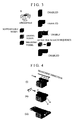
- Fig. 3 is a schematic diagram illustrating drawing of the 3D nanostructure by the supportable-voxel search method according to the present invention
- Fig. 4 is a schematic diagram illustrating the drawing order of the supportable-voxel search method according to the present invention.
- a supportable voxel (gray) is present in the five positions surrounding the drawing voxel B. If the supportable voxel is present in any one of the five positions, the drawing voxel is enabled. The drawn voxel does not simply turn to be the supportable voxel. It is because the supportable voxel has to satisfy certain conditions.
- the result of searching the structure similar to that used in the surround-voxel search method applying the supportable-voxel search method is as shown in Fig. 4. That is, the search starts from the upstream of an arrow indicating the searching direction, as shown in Fig. 4, to draw the base portion. In this process, the overhang portion on the upstream is left undrawn because the portion has no supporting base in the vicinity thereof.
- the area having the base (voxels 31, 32, and 33) is enabled.
- Fig. 4 The result of searching the structure similar to that used in the surround-voxel search method applying the supportable-voxel search method is as shown in Fig. 4. That is, the search starts from the upstream of an arrow indicating the searching direction, as shown in Fig. 4, to draw the base portion. In this
- the voxel (voxel 42) on the upstream is enabled in the second round of searching.
- the overhang portion is drawn in the direction parallel to the base and extending outwardly.
- the similar orders and directions of drawing are applied on the upstream and downstream of searching.
- Fig. 5 shows a drawn result by the surround-voxel search method according to the present invention.
- the drawing is performed by applying the surround-voxel search method to a 3D drawing apparatus.
- the drawing density is represented by overlapping (%) of the diameter on the basis of the effective deposition diameter (that is, the pillar diameter).
- the irradiation pitch is 3 nm.
- the searching direction is from the right to the left on the paper.
- the irradiation pitch is made narrower from 95% to 98%, the deposition on the substrate on the upstream of searching (the right side) becomes less, resulting in the better condition.
- the deposition on the substrate or the side surface of the pillar is still found on the downstream of searching (the left side). It is apparently because of the asymmetrical characteristics of the directions and orders of drawing on the upstream and downstream, as described above.
- Fig. 6 shows a drawn result by the supportable-voxel search method according to the present invention.
- Fig. 6 shows the result using the similar method to that applied in Fig. 5 by changing the drawing pitch from 95% to 98%. While the upstream of searching exhibits good result with less deposition on the substrate when the irradiation pitch is narrowed from 95% to 98%, the both sides exhibit similar deposition results with substantially no deposition on the substrate or the side surface of the pillar at the irradiation pitch of 98%. The symmetric characteristics of the direction and order of drawing of the supportable-voxel search method are apparently brought out. However, it is understood that the upstream exhibits the better deposition result. It does not depend on the difference in the amount of gas flow, examined by exchanging the X- and Y-axes.
- Fig. 7 is a block diagram of a fabrication apparatus of the 3D nanostructure illustrating the embodiment of the present invention
- Fig. 8 is an SIM image of a compound-eye microlens mold fabricated by a drawing apparatus illustrating the embodiment of the present invention
- Fig. 9 is an SIM image of a microring with a diameter of approximately 4.2 ⁇ m.
- reference numeral 101 denotes an Si substrate
- 102 denotes a DLC (Diamond Like Carbon) pillar as a deposition structure
- 103 denotes the 3D nanostructure formed on the DLC pillar 102
- 104 denotes a gas nozzle to inject phenanthrene gas (a melting point: 99 °C, a boiling point: 340 °C) as a reaction gas
- 105 denotes the phenanthrene gas
- 106 denotes an FIB apparatus
- 107 denotes the FIB
- 108 denotes a scanning direction of the FIB 107
- 109 denotes a computer-controlled drawing device, which is provided with a CPU (Central Processing Unit) 109A, interfaces 109B and 109D, a memory 109C prestoring 3D positional data, a beam irradiation position, an irradiation direction and an irradiation time, an input/output device 109E, and a display device
- the arbitrary 3D structure can be fabricated using the focused ion beam (FIB).
- the arbitrary 3D structure was fabricated by converting a surface model created by a 3D-CAD into scan data, followed by drawing the structure discretely using FIB-CVD.
- the amount of deposition is controlled by changing the dwell time, the amount of the beam current, or a drawing interval of the ion beam 107 irradiated on the substrate 101.
- the drawing apparatus of the present invention targets on fabricating the 3D structure having the overhang shape as the end goal, that can be achieved using a vector-scan method.
- a 3D-DLC structure was fabricated by irradiating the Ga + ion beam 107 on the Si substrate 101 in the phenanthrene gas 105 atmosphere.
- Fig. 8 is the SIM image of the compound-eye microlens mold fabricated using the drawing apparatus of the present invention.
- the lens takes a semi-spherical shape with about 2.5 ⁇ m in diameter and about 0.8 ⁇ m in height.
- Fig. 9 is the SIM image of the microring with about 4.2 ⁇ m in diameter, wherein the overhang structure can be fabricated.
- the surface roughness of the 3D structure can be controlled at the nm level by changing the drawing interval.
- Fig. 10 is the SIM image illustrating the 3D nanostructure (spaceship shape) fabricated using the drawing apparatus of the present invention.
- the 3D nanostructure of the spaceship shape is formed by fabricating the pillar structure with a diameter of about 0.8 ⁇ m using the phenanthrene gas irradiated on the Si substrate, followed by fabricating a horizontal plate structure. And then, the overhang structure having a disc-like shape with a diameter of about 8 ⁇ m is fabricated.
- the fabrication condition was: a 30 kV Ga + ion beam, the beam current of about 10 pA, and the fabrication time of about 1 hour.
- the drawing data of the structure is indicated by the digital points and thus the surface roughness of the 3D structure formed by FIB-CVD depends on the resolution of a digital-analog converter (D/A converter). Therefore, to realize the surface smoothness of the 3D structure by increasing the resolution, an analog interpolation is performed sequentially for the data between the digital data points. That is, in the drawing method of the 3D structure according to the present invention, it is preferable to realize the surface smoothness of the 3D structure using the analog interpolation method to perform the analog interpolation between the points drawn by the 3D digital drawing method.
- a raster-scan method shown in Fig. 11, for example is the common scanning method which scans every point, it takes time to fabricate the structure due to the method requiring to scan every point. Since it is important to fabricate the structure in a short time when fabricated by FIB, the raster-scan method is not preferable.
- the vector-scan method as shown in Fig. 12, can reduce the time to fabricate the structure because the method only requires scanning the drawing points.
- the present invention applies the vector-scan method as the basic method for the drawing system.
- the present invention applies the method to sequentially interpolate the data between the discrete drawing points.
- the resolution higher than that of the D/A converter can be realized to improve the surface smoothness.
- the method using only the D/A converter can be referred to as a digital drawing method
- the method which can perform the analog interpolation of the data i.e., the analog interpolation method, is applied herein.
- the 3D structure obtained by the method of the present invention is characterized by being the 3D structure having the terrace or hollow structure in the ⁇ m to nm order.
- the 3D nanostructured mold can be an example of the 3D nanostructure having the hollow structure.
- a 3D microcube mold without the hollow structure can be fabricated.
- the 3D nanostructure including the terrace or hollow structure in the ⁇ m to nm order can be fabricated with the arbitrary size, shape, and surface roughness. Therefore, micro optical elements such as the microlens, micro mechanical elements such as nanotweezers, or a microsystem can be fabricated.
- the fabrication method of the 3D nanostructure and the drawing system of the 3D nanostructure by FIB-CVD according to the present invention are suitable for the 3D nanostructure or a fabrication tool of the 3D nanostructured mold which enables the fabrication of the 3D nanostructure having the terrace or hollow structure in the ⁇ m or nm order with the arbitrary size, shape, or surface roughness.
Landscapes
- Chemical & Material Sciences (AREA)
- Engineering & Computer Science (AREA)
- Materials Engineering (AREA)
- Manufacturing & Machinery (AREA)
- Organic Chemistry (AREA)
- Metallurgy (AREA)
- Mechanical Engineering (AREA)
- General Chemical & Material Sciences (AREA)
- Chemical Kinetics & Catalysis (AREA)
- Microelectronics & Electronic Packaging (AREA)
- Analytical Chemistry (AREA)
- Toxicology (AREA)
- Health & Medical Sciences (AREA)
- Physics & Mathematics (AREA)
- Plasma & Fusion (AREA)
- Chemical Vapour Deposition (AREA)
- Micromachines (AREA)
- Image Generation (AREA)
Abstract
Description
Claims (7)
- A method of fabricating a three-dimensional nanostructure by FIB-CVD, wherein a focused ion beam is controlled to determine a beam irradiation position or time based on discrete drawing data of a multilayer structure generated by calculating a cross-sectional shape divided in a vertical direction of a three-dimensional nanostructure model designed using an electronic computer.
- The method of fabricating the three-dimensional nanostructure by FIB-CVD according to Claim 1, wherein a height of a layer, surface roughness or a fabrication time of the multilayer structure is controlled by controlling a beam intensity, an irradiation time, or a time interval of irradiation.
- The method of fabricating the three-dimensional nanostructure by FIB-CVD according to Claim 1, wherein a hollow structure without a support underneath is fabricated by sorting a drawing order of the discrete drawing data by a condition of whether a supporting layer being present underneath.
- The method of fabricating the three-dimensional nanostructure by FIB-CVD according to Claim 1, wherein surface smoothness of the nanostructure due to increased resolution is realized by performing an analog interpolation sequentially for data between digital data points as drawing data.
- The method of fabricating the three-dimensional nanostructure by FIB-CVD according to Claim 1, wherein the three-dimensional nanostructure is the three-dimensional nanostructure having a terrace or hollow structure in the µm to nm order.
- The method of fabricating the three-dimensional nanostructure by FIB-CVD according to Claim 1 or 5, wherein the three-dimensional nanostructure is a three-dimensionally nanostructured mold.
- A drawing system of a three-dimensional nanostructure by FIB-CVD, wherein drawing of a three-dimensionally divided model incorporating a growing mode depending on a spatial drawing position is performed, to realize the free-designed three-dimensional drawing by FIB-CVD using the method of fabricating the three-dimensional nanostructure by FIB-CVD according to Claim 1.
Applications Claiming Priority (3)
| Application Number | Priority Date | Filing Date | Title |
|---|---|---|---|
| JP2003054361 | 2003-02-28 | ||
| JP2003054361 | 2003-02-28 | ||
| PCT/JP2004/001626 WO2004076343A1 (en) | 2003-02-28 | 2004-02-16 | Method for fabricating three-dimensional microstructure by fib-cvd and drawing system for three-dimensional microstructure |
Publications (2)
| Publication Number | Publication Date |
|---|---|
| EP1598312A1 true EP1598312A1 (en) | 2005-11-23 |
| EP1598312A4 EP1598312A4 (en) | 2008-03-26 |
Family
ID=32923459
Family Applications (1)
| Application Number | Title | Priority Date | Filing Date |
|---|---|---|---|
| EP04711478A Withdrawn EP1598312A4 (en) | 2003-02-28 | 2004-02-16 | METHOD FOR MANUFACTURING A THREE DIMENSIONAL MICROSTRUCTURE BY FIB-CVC AND SYSTEM FOR DRAWING THE MICROSTRUCTURE |
Country Status (7)
| Country | Link |
|---|---|
| US (1) | US20060292709A1 (en) |
| EP (1) | EP1598312A4 (en) |
| JP (1) | JP4269028B2 (en) |
| KR (1) | KR100709514B1 (en) |
| CN (1) | CN100415636C (en) |
| TW (1) | TWI244463B (en) |
| WO (1) | WO2004076343A1 (en) |
Cited By (1)
| Publication number | Priority date | Publication date | Assignee | Title |
|---|---|---|---|---|
| WO2010112827A3 (en) * | 2009-03-31 | 2010-12-02 | The Secretary Of State For Business Innovation And Skills Of Her Majesty's Britannic Government | Method and apparatus for producing three dimensional nano and micro scale structures |
Families Citing this family (16)
| Publication number | Priority date | Publication date | Assignee | Title |
|---|---|---|---|---|
| JP4485323B2 (en) * | 2004-11-04 | 2010-06-23 | 独立行政法人科学技術振興機構 | Method for manufacturing nerve regeneration electrode device and nerve regeneration electrode device |
| JP2007069325A (en) * | 2005-09-08 | 2007-03-22 | Japan Science & Technology Agency | Manufacturing method of micro electromagnetic device and micro electromagnetic device manufactured thereby |
| JP2007069329A (en) * | 2005-09-08 | 2007-03-22 | Japan Science & Technology Agency | Manufacturing method of micro three-dimensional structure operation tool and micro three-dimensional structure operation tool manufactured thereby |
| JP4672534B2 (en) * | 2005-11-29 | 2011-04-20 | 独立行政法人科学技術振興機構 | Micro electron emitter fabrication method and micro electron emitter fabricated using the same |
| KR100936114B1 (en) * | 2008-02-18 | 2010-01-11 | 연세대학교 산학협력단 | Manufacturing method of nanosensor using airborne nanowires formed by focused ion beam-chemical vapor deposition |
| US20150013901A1 (en) * | 2013-07-11 | 2015-01-15 | Hsio Technologies, Llc | Matrix defined electrical circuit structure |
| CN103924192A (en) * | 2014-04-21 | 2014-07-16 | 上海理工大学 | Preparation method of metallic silver thin film with nanometer microcavity structure |
| WO2016057034A1 (en) | 2014-10-08 | 2016-04-14 | Hewlett-Packard Development Company, L.P. | Fabricating a three-dimensional object |
| EP3151264A1 (en) * | 2015-10-02 | 2017-04-05 | FEI Company | Adaptive beam current for high throughput patterning |
| JP2017020106A (en) | 2015-07-02 | 2017-01-26 | エフ・イ−・アイ・カンパニー | Adaptive beam current for high-throughput pattern formation |
| EP3159910A1 (en) * | 2015-10-20 | 2017-04-26 | FEI Company | Adaptive control for charged particle beam processing |
| US11534945B2 (en) * | 2018-11-26 | 2022-12-27 | Directed Energy Materials LLC | Bragg-peak three-dimensional manufacturing with resins |
| CN110605392B (en) * | 2019-09-24 | 2020-06-30 | 浙江大学 | Metal entity printing method for alternately performing outer wall surfacing and internal filling |
| CN113390914B (en) * | 2020-03-13 | 2022-10-14 | 中国科学院上海硅酸盐研究所 | Method for representing three-dimensional microstructure of ceramic coating material based on focused ion beam |
| CN111646428B (en) * | 2020-06-15 | 2023-03-10 | 河南大学 | A method for constructing 3D micro/nanostructures |
| CN113865958A (en) * | 2021-09-22 | 2021-12-31 | 卡尔蔡司(上海)管理有限公司 | Method for producing three-dimensional structures |
Family Cites Families (12)
| Publication number | Priority date | Publication date | Assignee | Title |
|---|---|---|---|---|
| US4983830A (en) * | 1989-06-29 | 1991-01-08 | Seiko Instruments Inc. | Focused ion beam apparatus having charged particle energy filter |
| US5017317A (en) * | 1989-12-04 | 1991-05-21 | Board Of Regents, The Uni. Of Texas System | Gas phase selective beam deposition |
| US5504340A (en) * | 1993-03-10 | 1996-04-02 | Hitachi, Ltd. | Process method and apparatus using focused ion beam generating means |
| JP4137317B2 (en) * | 1999-10-07 | 2008-08-20 | 独立行政法人科学技術振興機構 | Micro three-dimensional structure, manufacturing method thereof, and manufacturing apparatus thereof |
| JP4223672B2 (en) * | 2000-10-31 | 2009-02-12 | エスアイアイ・ナノテクノロジー株式会社 | Beam-shaped film pattern forming method |
| JP4704595B2 (en) * | 2001-04-17 | 2011-06-15 | エスアイアイ・ナノテクノロジー株式会社 | Method of growing fine three-dimensional structure by CVD and focused ion beam apparatus |
| JP4199440B2 (en) * | 2001-06-29 | 2008-12-17 | 日本電気株式会社 | Method for forming ultra-strength elastic diamond-like carbon |
| JP4688400B2 (en) * | 2001-12-04 | 2011-05-25 | エスアイアイ・ナノテクノロジー株式会社 | Probe for scanning probe microscope |
| US6887450B2 (en) * | 2002-01-02 | 2005-05-03 | Zyvex Corporation | Directional assembly of carbon nanotube strings |
| US8093144B2 (en) * | 2002-05-24 | 2012-01-10 | Massachusetts Institute Of Technology | Patterning of nanostructures |
| JP2004209626A (en) * | 2002-11-14 | 2004-07-29 | Seiko Instruments Inc | Three-dimensional microstructure manufacturing method and manufacturing apparatus |
| JP4936530B2 (en) * | 2007-05-15 | 2012-05-23 | キヤノン株式会社 | Manufacturing method of three-dimensional photonic crystal |
-
2004
- 2004-02-16 KR KR1020057016114A patent/KR100709514B1/en not_active Expired - Fee Related
- 2004-02-16 CN CNB2004800081234A patent/CN100415636C/en not_active Expired - Fee Related
- 2004-02-16 JP JP2005502831A patent/JP4269028B2/en not_active Expired - Fee Related
- 2004-02-16 WO PCT/JP2004/001626 patent/WO2004076343A1/en not_active Ceased
- 2004-02-16 US US10/546,988 patent/US20060292709A1/en not_active Abandoned
- 2004-02-16 EP EP04711478A patent/EP1598312A4/en not_active Withdrawn
- 2004-02-18 TW TW093103842A patent/TWI244463B/en not_active IP Right Cessation
Cited By (1)
| Publication number | Priority date | Publication date | Assignee | Title |
|---|---|---|---|---|
| WO2010112827A3 (en) * | 2009-03-31 | 2010-12-02 | The Secretary Of State For Business Innovation And Skills Of Her Majesty's Britannic Government | Method and apparatus for producing three dimensional nano and micro scale structures |
Also Published As
| Publication number | Publication date |
|---|---|
| US20060292709A1 (en) | 2006-12-28 |
| CN1764596A (en) | 2006-04-26 |
| CN100415636C (en) | 2008-09-03 |
| TWI244463B (en) | 2005-12-01 |
| WO2004076343A1 (en) | 2004-09-10 |
| KR20050107475A (en) | 2005-11-11 |
| JP4269028B2 (en) | 2009-05-27 |
| TW200417507A (en) | 2004-09-16 |
| KR100709514B1 (en) | 2007-04-20 |
| JPWO2004076343A1 (en) | 2006-06-01 |
| EP1598312A4 (en) | 2008-03-26 |
Similar Documents
| Publication | Publication Date | Title |
|---|---|---|
| US20060292709A1 (en) | Method for fabricatiing three-dimensional microstructure by fib-cvd and drawing system for three-dimensional microstruture | |
| Bruchhaus et al. | Comparison of technologies for nano device prototyping with a special focus on ion beams: A review | |
| JP4137317B2 (en) | Micro three-dimensional structure, manufacturing method thereof, and manufacturing apparatus thereof | |
| Xie et al. | Development of three-dimensional atomic force microscope for sidewall structures imaging with controllable scanning density | |
| US7267731B2 (en) | Method and system for fabricating three-dimensional microstructure | |
| CN101746709B (en) | Method for forming microscopic structures on a substrate | |
| US20070207318A1 (en) | Catalytically Grown Mano-Bent Nanostructure and Method for Making the Same | |
| CN100467367C (en) | Carbon nanotube array structure and preparation method thereof | |
| Wu et al. | An intelligent AFM scanning strategy based on autonomous exploration | |
| JP2005083857A (en) | Nanotube probe and manufacturing method | |
| CN107365979A (en) | Nano object deposits the attachment of structure to beam | |
| Jenke et al. | Toward local growth of individual nanowires on three-dimensional microstructures by using a minimally invasive catalyst templating method | |
| KR101411332B1 (en) | Implanted-ion assisted growth method of metal oxide Nanowire and pattening device using the method | |
| EP1141753B1 (en) | Method for producing optical fibers with subwavelength apertures | |
| US6600856B1 (en) | Lensed optical fibers and unique micropipettes with subwavelength apertures | |
| JP5032546B2 (en) | Method for manufacturing scanning microsensor having scanning tip and alignment mark on back surface thereof | |
| Fadaly | Epitaxy of Hexagonal SiGe Alloys for Light Emission | |
| Ritter | A landmark-based method for the geometrical 3D calibration of scanning microscopes | |
| Lee et al. | InAs Nanowires Elevated on Si (001) by Nanopedestals for CMOS-Compatible Fabrication | |
| Gott | Defects in self-catalysed III-V nanowires | |
| Bespalova | Experimental measurement of Young’s modulus of gallium phosphide nanowires by atomic force microscopy | |
| Matsui | Focuse Elecoconced | |
| Lee et al. | In-situ fabrication of nanostructures by photo-enhanced chemical vapor deposition using optical near field | |
| Kaito | Three-Dimensional Nanofabrication Using Focused Ion Beams | |
| Xu | Localized growth and characterization of silicon nanowires |
Legal Events
| Date | Code | Title | Description |
|---|---|---|---|
| PUAI | Public reference made under article 153(3) epc to a published international application that has entered the european phase |
Free format text: ORIGINAL CODE: 0009012 |
|
| 17P | Request for examination filed |
Effective date: 20050825 |
|
| AK | Designated contracting states |
Kind code of ref document: A1 Designated state(s): AT BE BG CH CY CZ DE DK EE ES FI FR GB GR HU IE IT LI LU MC NL PT RO SE SI SK TR |
|
| AX | Request for extension of the european patent |
Extension state: AL LT LV MK |
|
| DAX | Request for extension of the european patent (deleted) | ||
| RBV | Designated contracting states (corrected) |
Designated state(s): DE FR GB IT |
|
| RIN1 | Information on inventor provided before grant (corrected) |
Inventor name: KONDO, KAZUSHIGESEIKO INSTRUMENTS ASHIGARA Inventor name: MATSUI, SHINJI Inventor name: HOSHINO, TAKAYUKI |
|
| A4 | Supplementary search report drawn up and despatched |
Effective date: 20080222 |
|
| RAP1 | Party data changed (applicant data changed or rights of an application transferred) |
Owner name: MATSUI, SHINJI |
|
| 17Q | First examination report despatched |
Effective date: 20080806 |
|
| RAP1 | Party data changed (applicant data changed or rights of an application transferred) |
Owner name: SII NANOTECHNOLOGY INC. |
|
| STAA | Information on the status of an ep patent application or granted ep patent |
Free format text: STATUS: THE APPLICATION IS DEEMED TO BE WITHDRAWN |
|
| 18D | Application deemed to be withdrawn |
Effective date: 20090217 |