EP1596372A1 - Magnetic recording media - Google Patents
Magnetic recording media Download PDFInfo
- Publication number
- EP1596372A1 EP1596372A1 EP04255243A EP04255243A EP1596372A1 EP 1596372 A1 EP1596372 A1 EP 1596372A1 EP 04255243 A EP04255243 A EP 04255243A EP 04255243 A EP04255243 A EP 04255243A EP 1596372 A1 EP1596372 A1 EP 1596372A1
- Authority
- EP
- European Patent Office
- Prior art keywords
- underlayer
- interlayer
- overlayer
- magnetic recording
- oxide
- Prior art date
- Legal status (The legal status is an assumption and is not a legal conclusion. Google has not performed a legal analysis and makes no representation as to the accuracy of the status listed.)
- Withdrawn
Links
- 239000010410 layer Substances 0.000 claims abstract description 115
- 239000011229 interlayer Substances 0.000 claims abstract description 74
- 229910045601 alloy Inorganic materials 0.000 claims abstract description 49
- 239000000956 alloy Substances 0.000 claims abstract description 49
- 229910052751 metal Inorganic materials 0.000 claims abstract description 36
- 239000002184 metal Substances 0.000 claims abstract description 36
- 239000000758 substrate Substances 0.000 claims abstract description 30
- 230000003647 oxidation Effects 0.000 claims abstract description 28
- 238000007254 oxidation reaction Methods 0.000 claims abstract description 28
- 238000004544 sputter deposition Methods 0.000 claims abstract description 26
- 238000000034 method Methods 0.000 claims abstract description 24
- QVGXLLKOCUKJST-UHFFFAOYSA-N atomic oxygen Chemical compound [O] QVGXLLKOCUKJST-UHFFFAOYSA-N 0.000 claims abstract description 22
- 229910052760 oxygen Inorganic materials 0.000 claims abstract description 22
- 239000001301 oxygen Substances 0.000 claims abstract description 22
- 238000004519 manufacturing process Methods 0.000 claims abstract description 15
- 239000000314 lubricant Substances 0.000 claims description 20
- 229910052791 calcium Inorganic materials 0.000 claims description 7
- 229910052712 strontium Inorganic materials 0.000 claims description 7
- 229910052746 lanthanum Inorganic materials 0.000 claims description 6
- 229910052744 lithium Inorganic materials 0.000 claims description 6
- 229910052749 magnesium Inorganic materials 0.000 claims description 6
- 229910052748 manganese Inorganic materials 0.000 claims description 6
- 229910052758 niobium Inorganic materials 0.000 claims description 6
- 229910052700 potassium Inorganic materials 0.000 claims description 6
- 229910052706 scandium Inorganic materials 0.000 claims description 6
- 229910052708 sodium Inorganic materials 0.000 claims description 6
- 229910052719 titanium Inorganic materials 0.000 claims description 6
- 229910052720 vanadium Inorganic materials 0.000 claims description 6
- 229910052727 yttrium Inorganic materials 0.000 claims description 6
- 229910052726 zirconium Inorganic materials 0.000 claims description 6
- 239000010409 thin film Substances 0.000 description 47
- 239000002245 particle Substances 0.000 description 17
- 239000000463 material Substances 0.000 description 15
- 239000011651 chromium Substances 0.000 description 13
- 150000002739 metals Chemical class 0.000 description 12
- 208000037824 growth disorder Diseases 0.000 description 11
- 238000000151 deposition Methods 0.000 description 9
- 239000002019 doping agent Substances 0.000 description 9
- 238000010899 nucleation Methods 0.000 description 9
- 230000000694 effects Effects 0.000 description 8
- 230000006911 nucleation Effects 0.000 description 8
- 229910001149 41xx steel Inorganic materials 0.000 description 7
- 239000010408 film Substances 0.000 description 7
- 239000000843 powder Substances 0.000 description 7
- 230000009286 beneficial effect Effects 0.000 description 5
- OKTJSMMVPCPJKN-UHFFFAOYSA-N Carbon Chemical compound [C] OKTJSMMVPCPJKN-UHFFFAOYSA-N 0.000 description 4
- 229910000943 NiAl Inorganic materials 0.000 description 4
- NPXOKRUENSOPAO-UHFFFAOYSA-N Raney nickel Chemical compound [Al].[Ni] NPXOKRUENSOPAO-UHFFFAOYSA-N 0.000 description 4
- 229910052799 carbon Inorganic materials 0.000 description 4
- 238000013500 data storage Methods 0.000 description 4
- 230000008021 deposition Effects 0.000 description 4
- 239000000203 mixture Substances 0.000 description 4
- 238000005546 reactive sputtering Methods 0.000 description 4
- 230000008901 benefit Effects 0.000 description 3
- 238000005266 casting Methods 0.000 description 3
- 229910017052 cobalt Inorganic materials 0.000 description 3
- 239000010941 cobalt Substances 0.000 description 3
- GUTLYIVDDKVIGB-UHFFFAOYSA-N cobalt atom Chemical compound [Co] GUTLYIVDDKVIGB-UHFFFAOYSA-N 0.000 description 3
- 239000007789 gas Substances 0.000 description 3
- 238000001513 hot isostatic pressing Methods 0.000 description 3
- 230000008018 melting Effects 0.000 description 3
- 238000007670 refining Methods 0.000 description 3
- 238000005204 segregation Methods 0.000 description 3
- 238000003860 storage Methods 0.000 description 3
- VYZAMTAEIAYCRO-UHFFFAOYSA-N Chromium Chemical compound [Cr] VYZAMTAEIAYCRO-UHFFFAOYSA-N 0.000 description 2
- 229910000531 Co alloy Inorganic materials 0.000 description 2
- VYPSYNLAJGMNEJ-UHFFFAOYSA-N Silicium dioxide Chemical group O=[Si]=O VYPSYNLAJGMNEJ-UHFFFAOYSA-N 0.000 description 2
- 229910052782 aluminium Inorganic materials 0.000 description 2
- XAGFODPZIPBFFR-UHFFFAOYSA-N aluminium Chemical compound [Al] XAGFODPZIPBFFR-UHFFFAOYSA-N 0.000 description 2
- 229910052804 chromium Inorganic materials 0.000 description 2
- 150000001875 compounds Chemical class 0.000 description 2
- 238000005137 deposition process Methods 0.000 description 2
- 239000011521 glass Substances 0.000 description 2
- 238000002844 melting Methods 0.000 description 2
- 238000004663 powder metallurgy Methods 0.000 description 2
- 238000009987 spinning Methods 0.000 description 2
- 230000008961 swelling Effects 0.000 description 2
- 239000013077 target material Substances 0.000 description 2
- 239000011248 coating agent Substances 0.000 description 1
- 238000000576 coating method Methods 0.000 description 1
- 229910052681 coesite Inorganic materials 0.000 description 1
- 238000011109 contamination Methods 0.000 description 1
- 238000007796 conventional method Methods 0.000 description 1
- 229910052906 cristobalite Inorganic materials 0.000 description 1
- 230000007423 decrease Effects 0.000 description 1
- 238000000280 densification Methods 0.000 description 1
- 230000005684 electric field Effects 0.000 description 1
- 238000005516 engineering process Methods 0.000 description 1
- 239000011261 inert gas Substances 0.000 description 1
- 150000002500 ions Chemical class 0.000 description 1
- 238000002955 isolation Methods 0.000 description 1
- 229910001004 magnetic alloy Inorganic materials 0.000 description 1
- 238000010309 melting process Methods 0.000 description 1
- 229910044991 metal oxide Inorganic materials 0.000 description 1
- 150000004706 metal oxides Chemical class 0.000 description 1
- 238000012986 modification Methods 0.000 description 1
- 230000004048 modification Effects 0.000 description 1
- 230000000704 physical effect Effects 0.000 description 1
- 239000000376 reactant Substances 0.000 description 1
- 239000004065 semiconductor Substances 0.000 description 1
- 238000000926 separation method Methods 0.000 description 1
- 239000000377 silicon dioxide Substances 0.000 description 1
- 229910052682 stishovite Inorganic materials 0.000 description 1
- 238000000427 thin-film deposition Methods 0.000 description 1
- 229910052905 tridymite Inorganic materials 0.000 description 1
Images


Classifications
-
- G—PHYSICS
- G11—INFORMATION STORAGE
- G11B—INFORMATION STORAGE BASED ON RELATIVE MOVEMENT BETWEEN RECORD CARRIER AND TRANSDUCER
- G11B5/00—Recording by magnetisation or demagnetisation of a record carrier; Reproducing by magnetic means; Record carriers therefor
- G11B5/84—Processes or apparatus specially adapted for manufacturing record carriers
- G11B5/851—Coating a support with a magnetic layer by sputtering
-
- G—PHYSICS
- G11—INFORMATION STORAGE
- G11B—INFORMATION STORAGE BASED ON RELATIVE MOVEMENT BETWEEN RECORD CARRIER AND TRANSDUCER
- G11B5/00—Recording by magnetisation or demagnetisation of a record carrier; Reproducing by magnetic means; Record carriers therefor
- G11B5/62—Record carriers characterised by the selection of the material
- G11B5/64—Record carriers characterised by the selection of the material comprising only the magnetic material without bonding agent
- G11B5/65—Record carriers characterised by the selection of the material comprising only the magnetic material without bonding agent characterised by its composition
- G11B5/658—Record carriers characterised by the selection of the material comprising only the magnetic material without bonding agent characterised by its composition containing oxygen, e.g. molecular oxygen or magnetic oxide
-
- G—PHYSICS
- G11—INFORMATION STORAGE
- G11B—INFORMATION STORAGE BASED ON RELATIVE MOVEMENT BETWEEN RECORD CARRIER AND TRANSDUCER
- G11B5/00—Recording by magnetisation or demagnetisation of a record carrier; Reproducing by magnetic means; Record carriers therefor
- G11B5/62—Record carriers characterised by the selection of the material
- G11B5/73—Base layers, i.e. all non-magnetic layers lying under a lowermost magnetic recording layer, e.g. including any non-magnetic layer in between a first magnetic recording layer and either an underlying substrate or a soft magnetic underlayer
- G11B5/7368—Non-polymeric layer under the lowermost magnetic recording layer
- G11B5/7369—Two or more non-magnetic underlayers, e.g. seed layers or barrier layers
-
- G—PHYSICS
- G11—INFORMATION STORAGE
- G11B—INFORMATION STORAGE BASED ON RELATIVE MOVEMENT BETWEEN RECORD CARRIER AND TRANSDUCER
- G11B5/00—Recording by magnetisation or demagnetisation of a record carrier; Reproducing by magnetic means; Record carriers therefor
- G11B5/62—Record carriers characterised by the selection of the material
- G11B5/73—Base layers, i.e. all non-magnetic layers lying under a lowermost magnetic recording layer, e.g. including any non-magnetic layer in between a first magnetic recording layer and either an underlying substrate or a soft magnetic underlayer
- G11B5/7368—Non-polymeric layer under the lowermost magnetic recording layer
- G11B5/7379—Seed layer, e.g. at least one non-magnetic layer is specifically adapted as a seed or seeding layer
-
- G—PHYSICS
- G11—INFORMATION STORAGE
- G11B—INFORMATION STORAGE BASED ON RELATIVE MOVEMENT BETWEEN RECORD CARRIER AND TRANSDUCER
- G11B5/00—Recording by magnetisation or demagnetisation of a record carrier; Reproducing by magnetic means; Record carriers therefor
- G11B5/84—Processes or apparatus specially adapted for manufacturing record carriers
- G11B5/8404—Processes or apparatus specially adapted for manufacturing record carriers manufacturing base layers
Definitions
- the present invention relates generally to the field of sputtering and, more particularly to magnetic recording media and methods for manufacturing such media. Certain embodiments relate to refining the grain structure of magnetic recording media using nucleating oxide-particle doped thin film materials.
- sputtering is widely used in a variety of fields to provide thin film material deposition of a precisely controlled thickness with an atomically smooth surface, for example to coat semiconductors and/or to form films on surfaces of magnetic recording media.
- a cathodic sputter target is positioned in a vacuum chamber partially filled with an inert gas atmosphere, and is exposed to an electric field to generate a plasma. Ions within this plasma collide with a surface of the sputter target causing the sputter target to emit atoms from the sputter target surface.
- the voltage difference between the cathodic sputter target and an anodic substrate that is to be coated causes the emitted atoms to form the desired film on the surface of the substrate.
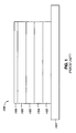
- FIG. 1 illustrates a typical thin film stack for conventional magnetic recording media.
- non-magnetic substrate 101 which is typically aluminum or glass.
- Seed layer 102 the first deposited layer, typically forces the shape and orientation of the grain structure of higher layers, and is commonly comprised of NiP or NiAl.
- a non-magnetic underlayer 104 which often includes one to three discrete layers, is deposited, where the underlayer is typically a chromium-based alloy, such as CrMo, or CrTi.
- Interlayer 105 which includes one or two separate layers, is formed above underlayer 104, where interlayer 105 is cobalt-based and slightly magnetic.
- Overlayer 106 which is magnetic and may include two or three separate layers, is deposited on top of interlayer 105, and carbon lubricant layer 108 is formed over overlayer 106.
- the amount of data that can be stored per unit area on a magnetic recording medium is inversely proportional to the size of the microstructure of the overlayer.
- Microstructure size corresponds to the size of a grain of the thin film, where a grain is a collection of molecules typically comprising 20 to 50 atoms.
- Microstructure uniformity a measure of the physical segregation of the grains, also contributes to increased data storage potential.
- One known technique for refining the grain size, and consequently increasing the storage potential of magnetic recording media is through the use of oxidic grain nucleation sites at the seed layer.
- an oxide particle deposited as a seed layer on the substrate acts as nucleating sites for subsequently deposited layers, reducing grain size and increasing data storage potential. Due to complexities in the sputter target manufacturing process, it is difficult to add oxides to a cast target, since the oxide particles are liberated from a parent metal during the melting and casting process. An alternate method of depositing an oxide particle film on a substrate to reduce grain size is therefore quite desirable.
- U.S. Patent Nos. 6,524,724 and 6,620,531 are seen to describe techniques for reducing grain size at the overlayer by depositing an oxide particle film as a seed layer, below the underlayer.
- an oxide particle film as a seed layer, below the underlayer.
- grain size in the additional layers also increases, and physical segregation between the grains decreases.
- oxide particle seeding techniques grain size at the underlayer may be reduced, but grain size at the overlayer tends to be markedly larger. Accordingly, conventional techniques for reducing grain size may have a beneficial effect on layers of the thin film stack adjacent to the seed layer, but the beneficial effect of oxide-doping the seed layer is mitigated in the overlayers, where grain size is most crucial.
- This invention seeks to provide improved magnetic recording media and methods for manufacturing same.
- the amount of data that can be stored per unit area on magnetic recording media corresponds to the grain density of the magnetic overlayer.
- nucleating oxide particles have been shown to effectively refine the microstructure of a thin film near the seed layer, several problems remain.
- certain embodiments of the present invention address disadvantages found in conventional sputter targets and sputter target manufacturing methods, particularly with those disadvantages which relate to the deposition of oxide-doped thin films and the densification of grains at the magnetic overlayer of a magnetic recording medium.
- the present invention is a magnetic recording medium.
- the magnetic recording medium includes a substrate, and at least a first underlayer formed over the substrate, where the first underlayer is comprised of a Cr-based alloy, such as CrMo or CrTi.
- the magnetic recording medium also includes at least a first interlayer formed over the first underlayer, where the first interlayer is comprised of a Co-based alloy, and at least a first overlayer formed over the first interlayer, where the first overlayer is magnetic and is comprised of a Co-based alloy.
- At least one of the first underlayer, the first interlayer and/or the first overlayer are doped with an X-oxide, where X is a metal with an oxidation potential of less than -0.6 eV.
- a magnetic recording medium embodying the present invention includes a refined microstructure with nucleating oxide sites contained within the thin film stack, where the thin film is sputtered from oxide-doped sputter target.
- Grain refinement can be applied to all layers of the magnetic stack, including any layer or layers of the underlayer, interlayer, and/or overlayer.
- nucleation sites can be sputtered on as a "flash" seed layer, which refines thin films which are to be sputtered above, or the nucleation sites may be contained within the thin films themselves.
- This type of refinement can be used for standard longitudinal media, vertical media, and anti-ferromagnetically-coupled (“AFC”) media, increasing storage density in most instances.
- AFC anti-ferromagnetically-coupled
- a lubricant layer is formed over the first overlayer, where the lubricant layer is comprised of C or a C-based alloy.
- the lubricant layer protects the overlayer from damage caused by physical contact between a read-write head and the overlayer itself, which may be spinning at thousands of rotations per minute.
- a seed layer is formed between the substrate and the first underlayer.
- a seed layer may be able to further reduce grain size and effectuate a uniform physical segregation of grains, by forcing the shape and orientation of the grain structure of subsequently deposited layers.
- a typical seed layer is comprised of NiP or NiAl.
- the at least one of the first underlayer, the first interlayer and/or the first overlayer comprise less than 4 At% X-oxide.
- One advantage of the present invention is that the nucleating oxide material need only comprise up to a small atomic percentage of the thin film, ensuring that physical properties of the thin film metal or alloy are otherwise not affected.
- X is a metal with a high oxidation potential, selected from the group consisting of Li, Na, K, Ca, Sr, Mg, Sc, Y, La, Ti, Zr, V, Nb, and Mn.
- the overall effect of the dopants and grain growth stunting is the same for each layer in the stack which contains the nucleating oxide materials.
- the sputter chamber needs no additional oxygen atmosphere, since the oxide is deposited alongside the parent metal or alloy, forcing grains to nucleate more readily and in greater numbers.
- a magnetic recording medium is manufactured by sputtering at least a first underlayer over a substrate layer, where the first underlayer is comprised of a Cr-based alloy, and sputtering at least a first interlayer over the first underlayer, where the first interlayer is comprised of a Co-based alloy, such as CoCrTa. Furthermore, the magnetic recording medium is manufactured by sputtering at least a first overlayer over the first interlayer, where the first overlayer is magnetic and is comprised of a Co-based alloy, such as CoCrPtB.
- At least one of the first underlayer, the first interlayer and/or the first overlayer are doped with X, where X is a metal with an oxidation potential of less than -0.6 eV.
- the at least one of the first underlayer, the first interlayer and/or the first overlayer are reactively sputtered in the presence of oxygen.
- Reactive sputtering is a deposition process in which species sputtered off the target material are chemically reacted with other species in the gas mixture to form a compound to be deposited, such as the case where Si is sputtered in plasma containing oxygen, resulting in the deposition of SiO 2 .
- a sputter target comprising a metal with a high oxidation potential is sputtered into a fine-grained oxide in a thin film, using either ambient, latent oxygen found naturally in the sputter chamber, or with controlled amounts of oxygen released into the chamber.
- the resulting deposited thin film has a refined grain size, enabled by the presence of fine oxide particles within the thin film.
- a magnetic recording medium is manufactured by sputtering at least a first underlayer over a substrate, where the first underlayer is comprised of a Cr-based alloy, and sputtering at least a first interlayer over the first underlayer, where the first interlayer is comprised of a Co-based alloy.
- the magnetic recording medium is manufactured by sputtering at least a first overlayer over the first interlayer, where the first overlayer is magnetic and is comprised of a Co-based alloy.
- At least one of the first underlayer, the first interlayer and/or the first overlayer are doped with an X-oxide, where X is a metal with an oxidation potential of less than -0.6 eV.
- the present invention is a magnetic recording medium.
- the magnetic recording medium at least a first underlayer formed over a substrate, where the first underlayer is comprised of a Cr-based alloy, such as CrMo or CrTi.
- the magnetic recording medium also includes at least a first interlayer formed over the first underlayer, where the first interlayer is comprised of a Co-based alloy, and at least a first overlayer formed over the first interlayer, where the first overlayer is magnetic and is comprised of a Co-based alloy.
- At least one of the first underlayer, the first interlayer and/or the first overlayer are doped with an X-oxide, where X is a metal with an oxidation potential of less than -0.6 eV.
- Embodiments of the present invention thus provide a magnetic recording medium with a dense grain structure at the overlayer, to increase potential data storage capabilities.
- Embodiments of the present invention allow for increased data storage of a magnetic recording medium by refining the grain size of the overlayer through oxide-particle doping of layers of the thin film stack which are deposited over a seed layer.
- the magnetic recording medium includes a substrate, and at least one underlayer formed over the substrate, where the underlayer is comprised of a Cr-based alloy, such as CrMo or CrTi.
- the magnetic recording medium also includes at least one interlayer formed over the underlayer, where the interlayer is comprised of a Co-based alloy, and at least one overlayer formed over the interlayer, where the overlayer is magnetic and is comprised of a Co-based alloy.
- At least one layer from the underlayer, the interlayer and/or the overlayer is doped with an X-oxide, where X is a metal with an oxidation potential of less than -0.6 eV.
- magnetic recording medium 400 includes substrate 401, which is typically aluminum or glass. Seed layer 402 is formed over substrate 401, where seed layer 402 forces the shape and orientation of the grain structure of subsequently deposited thin film layers. Typically, seed layer 402 is comprised of NiP or NiAl. In an alternate arrangements of the present invention, seed layer 402 is omitted.
- Underlayer 404 is formed over seed layer 402, or over substrate 401 if seed layer 402 is omitted. Although underlayer 404 is depicted as one layer, in an alternate aspect of the present invention underlayer 404 is three layers. Underlayer 404 is comprised of a chromium-based alloy, such as CrMo or CrTi, and may also further comprise an oxide.
- a chromium-based alloy such as CrMo or CrTi
- Interlayer 405 is formed over underlayer 404. Interlayer 405 is illustrated as one layer, however in an additional arrangement, interlayer 405 is three layers. Interlayer 405 is comprised of a cobalt-based alloy such as CoCrTa, and may also further comprise an oxide. Interlayer 406 is slightly magnetic.
- Overlayer 406 is formed over interlayer 405.
- overlayer 406 is shown as one layer.
- overlayer 405 is three layers.
- Overlayer 406 is comprised of a cobalt-based alloy such as CoCrPtB, and may also further comprise an oxide.
- Carbon lubricant layer 408 is formed over overlayer 406, where the lubricant layer is comprised of C or a C-based alloy. Carbon lubricant layer 408 protects overlayer 406 from damage caused by physical contact between a read-write head (not depicted) and overlayer 408 itself. In the alternate, carbon lubricant layer 408 is omitted.
- At least one layer from underlayer 404, interlayer 405 and/or overlayer 406 is doped with an X-oxide, where X is a metal with a high affinity for oxidation.
- X is a metal with a high affinity for oxidation.
- Metals with a high affinity for oxidation are metals with an oxidation potential of less than -0.6 eV. These metals effectuate the stunting of grain growth by depositing an oxide-doped nucleation site within a thin film.
- oxide-doping thin film layers above the seed layer the beneficial effect of grain growth stunting is not limited to layers which are adjacent to an oxide-doped seed layer.
- Table 1 lists several examples of stable and commercially available metals with a high affinity for oxidation. Table 1 is not an exhaustive list, but one of ordinary skill in the art would understand that metals having similar characteristics as those described below may also qualify as metals with a high affinity for oxidation.
- Element Oxidation Potential Li (to Li + ) -1.96 Na (to Na + ) -2.71 K (to K + ) -2.931 Ca (to Ca 2+ ) -2.868 Sr (to Sr 2+ ) -2.899 Mg (to Mg 2+ ) -2.372 Sc (to Sc 3+ ) -2.077 Y (to Y 3+ ) -2.372 La (to La 3+ ) -2.379 Ti (to Ti 2+ ) -1.630 Zr (to Zr 4+ ) -1.45 V (to V 2+ ) -1.175 Nb (to Nb 3+ ) -1.099 Mn (to Mn 2+ ) -1.185
- the magnetic recording medium includes a dense grain structure with nucleating oxide sites contained within the thin film stack above the seed layer, where the thin film is sputtered from oxide-doped sputter target.
- Grain refinement can be applied to all layers of the magnetic stack, including any layer or layers of the underlayer, interlayer, and/or overlayer. In each of these cases, nucleation sites can be sputtered on as a "flash" seed layer, which refines thin films which are to be sputtered above, or the nucleation sites may be contained within the thin films themselves. This type of refinement can be used for standard longitudinal media, vertical media, and AFC media, increasing storage density in most instances.
- the above-described thin films are deposited on substrate 401 utilizing sputtering processes recognized by those skilled in the material science art, using X-oxide doped sputter targets.
- Powder metallurgy is used to create these X-oxide doped sputter target, to avoid the problems relating to the liberation of oxygen from a parent metal during melting or casting.
- a mass of powder is formed into a shape or "can,” then consolidated to form inter-particle metallurgical bonds.
- elemental powders including an X-oxide powder
- X-oxide powder are mixed to produce a homogeneous blend
- the powders are encapsulated in a metal container, and the container is out-gassed to avoid contamination of the materials by any residual gas.
- a hot isostatic pressing (HIP) occurs on the container, in which heat and isostatic pressure are applied on the vessel to consolidate the powder, turning loose powder into a densified matter known as a "HIP'ed can.”
- the HIP'ed can is then machined, to create multiple X-oxide doped targets, which are then sputtered.
- the oxygen molecules are temporarily liberated from X, and remain within the vacuum chamber.
- the liberated oxygen molecules are attracted to X due to the high oxidation potential, and the X-oxide is reformed on the surface of the thin film.
- the sputter chamber needs no additional oxygen atmosphere, since the oxide is deposited alongside the parent metal or alloy, forcing grains to nucleate more readily and in greater numbers.
- X is selected from the group consisting of Li, Na, K, Ca, Sr, Mg, Sc, Y, La, Ti, Zr, V, Nb, and Mn.
- Metals with a high oxidation potential are more apt to remain in the oxide form, stunting grain grown rather than being absorbed into the totality of the parent phases.
- the overall effect of the dopants and grain growth stunting is the same for each layer in the stack which contains the nucleating oxide materials.
- Metal oxides can be added to existing alloys in quantities ranging from as little as 100 ppm, to several volume percent, depending on the thin film to be sputtered, and the dopant composition. Specifically, some alloys require only minute amounts of dopant to nucleate grains and retard grain growth, while other alloys will require larger quantities of dopant to achieve the same effect.
- the underlayer, interlayer and/or overlayer or layers which are doped with X-oxide comprise less than 4 At% X-oxide. The overall effect of the dopants and the grain growth stunting is the same for each layer in the stack which contains the nucleating oxide materials.
- SNR signal-to-noise ratio
- FIG. 5 is a flowchart which illustrates a method for manufacturing a magnetic recording medium, according to another aspect of the present invention.
- a magnetic recording medium is manufactured by sputtering at least one underlayer over a substrate layer, where the underlayer is comprised of a Cr-based alloy, and by sputtering at least one interlayer over the underlayer, where the interlayer is comprised of a Co-based alloy.
- the magnetic recording medium is manufactured by sputtering at least one overlayer over the interlayer, where the overlayer is comprised of a Co-based alloy.
- At least layer from the underlayer, the interlayer and/or the overlayer are doped with X, where X is a metal with an oxidation potential of less than -0.6 eV.
- the X-doped layer or layers are reactively sputtered in the presence of oxygen.
- the manufacturing process begins (step S501), and it is decided whether a seed layer should or should not be deposited (step S502).
- a seed layer typically comprised of NiP or NiAl, may be useful to force the shape and orientation of the grain structure of subsequently deposited layers. If a seed layer is desired, the seed layer is sputtered on a substrate (step S503). If a seed layer is not desired, a seed layer is not sputtered, and the process continues to step S504.
- An underlayer is sputtered over the seed layer, where the underlayer comprises a Cr-based alloy, such as CrMo or CrTi (step S504). Since thin film stacks often contain up to three underlayers, after the underlayer is sputtered it is decided whether an additional underlayer should or should not be deposited (step S505). If another underlayer is to be deposited, an additional underlayer is sputtered (step S504).
- a Cr-based alloy such as CrMo or CrTi
- step S506 If no more underlayers are to be deposited (step S505), an interlayer is sputtered (step S506).
- the interlayer is cobalt-based, and slightly magnetic. Since thin film stacks typically include two interlayers, after the interlayer is deposited it is determined whether to deposit an additional interlayer (step S507). If another interlayer is to be deposited, an additional interlayer is sputtered (step S506).
- a overlayer is sputtered (step S509). Typically, two or three of the cobalt-based overlayers are sputtered for each magnetic recording medium. If another overlayer is to be deposited (step S510), the additional overlayer is sputtered (step S509). Otherwise, it is determined whether a lubricant layer should be deposited (step S511).
- the lubricant layer is sputtered (step S512).
- a lubricant layer is formed over the first overlayer, where the lubricant layer is comprised of C or a C-based alloy.
- the lubricant layer protects the overlayer from damage caused by physical contact between a read-write had and the overlayer itself, which may be spinning at thousands of rotations per minute. If no lubricant layer is desired, of if a lubricant layer has already been deposited, the process ends (step S514).
- At least one layer from the interlayer, the underlayer, and/or the overlayer are doped with X, where X is a metal with an oxidation potential of less than -0.6 eV.
- X is a metal with an oxidation potential of less than -0.6 eV.
- the X-doped layer or layers are reactively sputtered in the presence of oxygen.
- Reactive sputtering is the deposition process in which a species, such as X, is sputtered off the target material and chemically reacted with other species, such as oxygen, in the gas mixture to form a compound to be deposited.
- a sputter target comprising a metal with a high affinity for oxidation is sputtered into a fine-grained oxide in a thin film, using either ambient, latent oxygen found naturally in the sputter chamber, or with controlled amounts of oxygen released into the chamber.
- the resulting deposited thin film has a refined grain size, enabled by the presence of fine oxide particles within the thin film.
- embodiments of the present invention facilitate the doping of high oxidation materials in thin films of magnetic recording material.
- one or more metals with high oxidation potential are included in the parent alloy or metal as dopants, in levels of 100 ppm up to several atomic percent. These metals are transformed upon sputtering into a fine-grained oxide form using either ambient, latent oxygen found naturally in small quantities in the sputter chamber, or with controlled amounts of oxygen released into the chamber.
- latent chamber oxygen or added oxygen will be determined by the type of dopant used, with more easily oxidized metals such as Sr or Ca requiring less oxygen to react.
- Layers which are not X-doped may be sputtered using conventional, non-reactive sputtering techniques.
- Metals with a high affinity for oxidation or with high oxidation potentials effectuate the stunting of grain growth by depositing an oxide-doped nucleation site within a thin film.
- oxide-doping thin film layers above the seed layer the beneficial effect of grain growth stunting is not limited to layers which are adjacent to an oxide-doped seed layer. Because of these advantages, grain grown is reduced because of the high density of grains, constraining swelling of each individual grain to under 60 ⁇ .
- At least one layer of the underlayer, the interlayer and/or the overlayer which is doped with X-oxide comprises less than 4 At% X-oxide.
- X is selected from the group consisting of Li, Na, K, Ca, Sr, Mg, Sc, Y, La, Ti, Zr, V, Nb, and Mn.
- the overall result of this method is a refinement of grain sizes, enabled by the presence of very small nucleating oxide particles, either on the surface of the substrate in a seed layer, or within the parent film itself, containing reactively-formed oxide particles.
- the columnar grains are markedly refined. If the thin film is X-doped, including the reactant inside the parent film, the grain structure may be improved, with the added benefit of improved grain separation, and improved SNR.
- a magnetic recording medium is manufactured by sputtering at least one underlayer over a substrate, where the underlayer is comprised of a Cr-based alloy, and sputtering at least one interlayer over the underlayer, where the interlayer is comprised of a Co-based alloy.
- the magnetic recording medium is manufactured by sputtering at least one overlayer over the interlayer, where the overlayer is comprised of a Co-based alloy.
- At least one layer of the underlayer, the interlayer and/or the overlayer are doped with an X-oxide, where X is a metal with an oxidation potential of less than -0.6 eV.
- a lubricant layer is formed over the first overlayer, where the lubricant layer is comprised of C or a C-based alloy.
- a seed layer is formed between the substrate and the first underlayer.
- the at least one of the first underlayer, the first interlayer and/or the first overlayer comprise less than 4 At% X-oxide. The overall effect of the dopants and grain growth stunting is the same for each layer in the stack which contains the nucleating oxide materials.
- X is selected from the group consisting of Li, Na, K, Ca, Sr, Mg, Sc, Y, La, Ti, Zr, V, Nb, and Mn.
- the present invention is a magnetic recording medium.
- the magnetic recording medium includes at least a first underlayer formed over a substrate, where the first underlayer is comprised of a Cr-based alloy, such as CrMo or CrTi.
- the magnetic recording medium also includes at least a first interlayer formed over the first underlayer, where the first interlayer is comprised of a Co-based alloy, and at least a first overlayer formed over the first interlayer, where the first overlayer is magnetic and is comprised of a Co-based alloy.
- At least one of the first underlayer, the first interlayer and/or the first overlayer are doped with an X-oxide, where X is a metal with an oxidation potential of less than -0.6 eV.
Abstract
Description
- The present invention relates generally to the field of sputtering and, more particularly to magnetic recording media and methods for manufacturing such media. Certain embodiments relate to refining the grain structure of magnetic recording media using nucleating oxide-particle doped thin film materials.
- The process of sputtering is widely used in a variety of fields to provide thin film material deposition of a precisely controlled thickness with an atomically smooth surface, for example to coat semiconductors and/or to form films on surfaces of magnetic recording media. In the sputtering process, a cathodic sputter target is positioned in a vacuum chamber partially filled with an inert gas atmosphere, and is exposed to an electric field to generate a plasma. Ions within this plasma collide with a surface of the sputter target causing the sputter target to emit atoms from the sputter target surface. The voltage difference between the cathodic sputter target and an anodic substrate that is to be coated causes the emitted atoms to form the desired film on the surface of the substrate.
- During the production of conventional magnetic recording media, layers of thin films are sequentially sputtered onto a substrate by multiple sputter targets, where each sputter target is comprised of a different material, resulting in the deposition of a thin film "stack." Figure 1 illustrates a typical thin film stack for conventional magnetic recording media. At the base of the stack is
non-magnetic substrate 101, which is typically aluminum or glass.Seed layer 102, the first deposited layer, typically forces the shape and orientation of the grain structure of higher layers, and is commonly comprised of NiP or NiAl. Next, anon-magnetic underlayer 104, which often includes one to three discrete layers, is deposited, where the underlayer is typically a chromium-based alloy, such as CrMo, or CrTi.Interlayer 105, which includes one or two separate layers, is formed aboveunderlayer 104, whereinterlayer 105 is cobalt-based and slightly magnetic.Overlayer 106, which is magnetic and may include two or three separate layers, is deposited on top ofinterlayer 105, andcarbon lubricant layer 108 is formed overoverlayer 106. - The amount of data that can be stored per unit area on a magnetic recording medium is inversely proportional to the size of the microstructure of the overlayer. Microstructure size corresponds to the size of a grain of the thin film, where a grain is a collection of molecules typically comprising 20 to 50 atoms. Microstructure uniformity, a measure of the physical segregation of the grains, also contributes to increased data storage potential.
- One known technique for refining the grain size, and consequently increasing the storage potential of magnetic recording media, is through the use of oxidic grain nucleation sites at the seed layer. As depicted in Figure 2, an oxide particle deposited as a seed layer on the substrate acts as nucleating sites for subsequently deposited layers, reducing grain size and increasing data storage potential. Due to complexities in the sputter target manufacturing process, it is difficult to add oxides to a cast target, since the oxide particles are liberated from a parent metal during the melting and casting process. An alternate method of depositing an oxide particle film on a substrate to reduce grain size is therefore quite desirable.
- U.S. Patent Nos. 6,524,724 and 6,620,531 are seen to describe techniques for reducing grain size at the overlayer by depositing an oxide particle film as a seed layer, below the underlayer. As depicted in Figure 3, as additional thin film layers are deposited on an oxide-particle enriched seed layer and the distance from the seed layer increases, grain size in the additional layers also increases, and physical segregation between the grains decreases. Using these oxide particle seeding techniques, grain size at the underlayer may be reduced, but grain size at the overlayer tends to be markedly larger. Accordingly, conventional techniques for reducing grain size may have a beneficial effect on layers of the thin film stack adjacent to the seed layer, but the beneficial effect of oxide-doping the seed layer is mitigated in the overlayers, where grain size is most crucial.
- This invention seeks to provide improved magnetic recording media and methods for manufacturing same.
- The amount of data that can be stored per unit area on magnetic recording media corresponds to the grain density of the magnetic overlayer. Although nucleating oxide particles have been shown to effectively refine the microstructure of a thin film near the seed layer, several problems remain. In this regard, certain embodiments of the present invention address disadvantages found in conventional sputter targets and sputter target manufacturing methods, particularly with those disadvantages which relate to the deposition of oxide-doped thin films and the densification of grains at the magnetic overlayer of a magnetic recording medium.
- According to one aspect, the present invention is a magnetic recording medium. The magnetic recording medium includes a substrate, and at least a first underlayer formed over the substrate, where the first underlayer is comprised of a Cr-based alloy, such as CrMo or CrTi. The magnetic recording medium also includes at least a first interlayer formed over the first underlayer, where the first interlayer is comprised of a Co-based alloy, and at least a first overlayer formed over the first interlayer, where the first overlayer is magnetic and is comprised of a Co-based alloy. At least one of the first underlayer, the first interlayer and/or the first overlayer are doped with an X-oxide, where X is a metal with an oxidation potential of less than -0.6 eV.
- A magnetic recording medium embodying the present invention includes a refined microstructure with nucleating oxide sites contained within the thin film stack, where the thin film is sputtered from oxide-doped sputter target. Grain refinement can be applied to all layers of the magnetic stack, including any layer or layers of the underlayer, interlayer, and/or overlayer. In each of these cases, nucleation sites can be sputtered on as a "flash" seed layer, which refines thin films which are to be sputtered above, or the nucleation sites may be contained within the thin films themselves. This type of refinement can be used for standard longitudinal media, vertical media, and anti-ferromagnetically-coupled ("AFC") media, increasing storage density in most instances.
- A lubricant layer is formed over the first overlayer, where the lubricant layer is comprised of C or a C-based alloy. The lubricant layer protects the overlayer from damage caused by physical contact between a read-write head and the overlayer itself, which may be spinning at thousands of rotations per minute.
- A seed layer is formed between the substrate and the first underlayer. A seed layer may be able to further reduce grain size and effectuate a uniform physical segregation of grains, by forcing the shape and orientation of the grain structure of subsequently deposited layers. A typical seed layer is comprised of NiP or NiAl.
- The at least one of the first underlayer, the first interlayer and/or the first overlayer comprise less than 4 At% X-oxide. One advantage of the present invention is that the nucleating oxide material need only comprise up to a small atomic percentage of the thin film, ensuring that physical properties of the thin film metal or alloy are otherwise not affected.
- X is a metal with a high oxidation potential, selected from the group consisting of Li, Na, K, Ca, Sr, Mg, Sc, Y, La, Ti, Zr, V, Nb, and Mn. The overall effect of the dopants and grain growth stunting is the same for each layer in the stack which contains the nucleating oxide materials. In the situation where X-oxide doped sputter targets are used to sputter nucleating oxide materials, the sputter chamber needs no additional oxygen atmosphere, since the oxide is deposited alongside the parent metal or alloy, forcing grains to nucleate more readily and in greater numbers.
- According to a second aspect of the present invention, a magnetic recording medium is manufactured by sputtering at least a first underlayer over a substrate layer, where the first underlayer is comprised of a Cr-based alloy, and sputtering at least a first interlayer over the first underlayer, where the first interlayer is comprised of a Co-based alloy, such as CoCrTa. Furthermore, the magnetic recording medium is manufactured by sputtering at least a first overlayer over the first interlayer, where the first overlayer is magnetic and is comprised of a Co-based alloy, such as CoCrPtB. At least one of the first underlayer, the first interlayer and/or the first overlayer are doped with X, where X is a metal with an oxidation potential of less than -0.6 eV. The at least one of the first underlayer, the first interlayer and/or the first overlayer are reactively sputtered in the presence of oxygen.
- Reactive sputtering is a deposition process in which species sputtered off the target material are chemically reacted with other species in the gas mixture to form a compound to be deposited, such as the case where Si is sputtered in plasma containing oxygen, resulting in the deposition of SiO2. Using the manufacturing method of the present invention, a sputter target comprising a metal with a high oxidation potential is sputtered into a fine-grained oxide in a thin film, using either ambient, latent oxygen found naturally in the sputter chamber, or with controlled amounts of oxygen released into the chamber. The resulting deposited thin film has a refined grain size, enabled by the presence of fine oxide particles within the thin film.
- According to a third aspect of the present invention, a magnetic recording medium is manufactured by sputtering at least a first underlayer over a substrate, where the first underlayer is comprised of a Cr-based alloy, and sputtering at least a first interlayer over the first underlayer, where the first interlayer is comprised of a Co-based alloy. Moreover, the magnetic recording medium is manufactured by sputtering at least a first overlayer over the first interlayer, where the first overlayer is magnetic and is comprised of a Co-based alloy. At least one of the first underlayer, the first interlayer and/or the first overlayer are doped with an X-oxide, where X is a metal with an oxidation potential of less than -0.6 eV.
- According to a fourth aspect, the present invention is a magnetic recording medium. The magnetic recording medium at least a first underlayer formed over a substrate, where the first underlayer is comprised of a Cr-based alloy, such as CrMo or CrTi. The magnetic recording medium also includes at least a first interlayer formed over the first underlayer, where the first interlayer is comprised of a Co-based alloy, and at least a first overlayer formed over the first interlayer, where the first overlayer is magnetic and is comprised of a Co-based alloy. At least one of the first underlayer, the first interlayer and/or the first overlayer are doped with an X-oxide, where X is a metal with an oxidation potential of less than -0.6 eV.
- Embodiments of the present invention thus provide a magnetic recording medium with a dense grain structure at the overlayer, to increase potential data storage capabilities. In particular, it is desirable to provide a method for sputtering a thin film stack, where the grain structure is controlled and made uniformly dense on layers of the thin film stack above the seed layer.
- In the following description of the preferred embodiment, reference is made to the accompanying drawings that form a part thereof, and in which is shown by way of illustration a specific embodiment in which the invention may be practiced. It is to be understood that other embodiments may be utilized and changes may be made without departing from the scope of the present invention.
- Referring now to the drawings in which like reference numbers represent corresponding parts throughout:
- Figure 1 depicts a typical thin film stack for conventional magnetic recording media;
- Figure 2 depicts the effect of conventional oxide particle doping of a seed layer on grain size;
- Figure 3 depicts the effect that distance from an oxide particle doped seed layer has on grain size;
- Figure 4 depicts a thin film stack according to one aspect of the present invention;
- Figure 5 is a flowchart which illustrates a method for manufacturing a magnetic recording medium, according to an additional aspect of the present invention; and
- Figure 6 illustrates the effect of reactive sputtering on thin film deposition, using a sputter target doped with a metal with a high oxidation potential sputtered in an oxygen-rich atmosphere.
-
- Embodiments of the present invention allow for increased data storage of a magnetic recording medium by refining the grain size of the overlayer through oxide-particle doping of layers of the thin film stack which are deposited over a seed layer.
- Figure 4 depicts a thin film stack of a magnetic recording medium according to one embodiment of the present invention. Briefly, the magnetic recording medium includes a substrate, and at least one underlayer formed over the substrate, where the underlayer is comprised of a Cr-based alloy, such as CrMo or CrTi. The magnetic recording medium also includes at least one interlayer formed over the underlayer, where the interlayer is comprised of a Co-based alloy, and at least one overlayer formed over the interlayer, where the overlayer is magnetic and is comprised of a Co-based alloy. At least one layer from the underlayer, the interlayer and/or the overlayer is doped with an X-oxide, where X is a metal with an oxidation potential of less than -0.6 eV.
- In more detail,
magnetic recording medium 400 includessubstrate 401, which is typically aluminum or glass.Seed layer 402 is formed oversubstrate 401, whereseed layer 402 forces the shape and orientation of the grain structure of subsequently deposited thin film layers. Typically,seed layer 402 is comprised of NiP or NiAl. In an alternate arrangements of the present invention,seed layer 402 is omitted. -
Underlayer 404 is formed overseed layer 402, or oversubstrate 401 ifseed layer 402 is omitted. Althoughunderlayer 404 is depicted as one layer, in an alternate aspect of thepresent invention underlayer 404 is three layers.Underlayer 404 is comprised of a chromium-based alloy, such as CrMo or CrTi, and may also further comprise an oxide. -
Interlayer 405 is formed overunderlayer 404.Interlayer 405 is illustrated as one layer, however in an additional arrangement,interlayer 405 is three layers.Interlayer 405 is comprised of a cobalt-based alloy such as CoCrTa, and may also further comprise an oxide.Interlayer 406 is slightly magnetic. -
Overlayer 406 is formed overinterlayer 405. In Figure 4,overlayer 406 is shown as one layer. In a further additional aspect of the present invention,overlayer 405 is three layers.Overlayer 406 is comprised of a cobalt-based alloy such as CoCrPtB, and may also further comprise an oxide. -
Carbon lubricant layer 408 is formed overoverlayer 406, where the lubricant layer is comprised of C or a C-based alloy.Carbon lubricant layer 408 protectsoverlayer 406 from damage caused by physical contact between a read-write head (not depicted) andoverlayer 408 itself. In the alternate,carbon lubricant layer 408 is omitted. - At least one layer from
underlayer 404,interlayer 405 and/oroverlayer 406 is doped with an X-oxide, where X is a metal with a high affinity for oxidation. Metals with a high affinity for oxidation are metals with an oxidation potential of less than -0.6 eV. These metals effectuate the stunting of grain growth by depositing an oxide-doped nucleation site within a thin film. By oxide-doping thin film layers above the seed layer, the beneficial effect of grain growth stunting is not limited to layers which are adjacent to an oxide-doped seed layer. - Table 1 lists several examples of stable and commercially available metals with a high affinity for oxidation. Table 1 is not an exhaustive list, but one of ordinary skill in the art would understand that metals having similar characteristics as those described below may also qualify as metals with a high affinity for oxidation.
Element Oxidation Potential (E°/V) Li (to Li+) -1.96 Na (to Na+) -2.71 K (to K+) -2.931 Ca (to Ca2+) -2.868 Sr (to Sr2+) -2.899 Mg (to Mg2+) -2.372 Sc (to Sc3+) -2.077 Y (to Y3+) -2.372 La (to La3+) -2.379 Ti (to Ti2+) -1.630 Zr (to Zr4+) -1.45 V (to V2+) -1.175 Nb (to Nb3+) -1.099 Mn (to Mn2+) -1.185 - The magnetic recording medium includes a dense grain structure with nucleating oxide sites contained within the thin film stack above the seed layer, where the thin film is sputtered from oxide-doped sputter target. Grain refinement can be applied to all layers of the magnetic stack, including any layer or layers of the underlayer, interlayer, and/or overlayer. In each of these cases, nucleation sites can be sputtered on as a "flash" seed layer, which refines thin films which are to be sputtered above, or the nucleation sites may be contained within the thin films themselves. This type of refinement can be used for standard longitudinal media, vertical media, and AFC media, increasing storage density in most instances.
- The above-described thin films are deposited on
substrate 401 utilizing sputtering processes recognized by those skilled in the material science art, using X-oxide doped sputter targets. Powder metallurgy is used to create these X-oxide doped sputter target, to avoid the problems relating to the liberation of oxygen from a parent metal during melting or casting. Using powder metallurgy, a mass of powder is formed into a shape or "can," then consolidated to form inter-particle metallurgical bonds. In more detail, elemental powders, including an X-oxide powder, are mixed to produce a homogeneous blend, the powders are encapsulated in a metal container, and the container is out-gassed to avoid contamination of the materials by any residual gas. A hot isostatic pressing (HIP) occurs on the container, in which heat and isostatic pressure are applied on the vessel to consolidate the powder, turning loose powder into a densified matter known as a "HIP'ed can." The HIP'ed can is then machined, to create multiple X-oxide doped targets, which are then sputtered. - During sputtering, the oxygen molecules are temporarily liberated from X, and remain within the vacuum chamber. When X deposits as a thin film on the substrate, the liberated oxygen molecules are attracted to X due to the high oxidation potential, and the X-oxide is reformed on the surface of the thin film. In the situation where X-oxide doped sputter targets are used to sputter nucleating oxide materials, the sputter chamber needs no additional oxygen atmosphere, since the oxide is deposited alongside the parent metal or alloy, forcing grains to nucleate more readily and in greater numbers.
- X is selected from the group consisting of Li, Na, K, Ca, Sr, Mg, Sc, Y, La, Ti, Zr, V, Nb, and Mn. Metals with a high oxidation potential are more apt to remain in the oxide form, stunting grain grown rather than being absorbed into the totality of the parent phases. The overall effect of the dopants and grain growth stunting is the same for each layer in the stack which contains the nucleating oxide materials.
- Metal oxides can be added to existing alloys in quantities ranging from as little as 100 ppm, to several volume percent, depending on the thin film to be sputtered, and the dopant composition. Specifically, some alloys require only minute amounts of dopant to nucleate grains and retard grain growth, while other alloys will require larger quantities of dopant to achieve the same effect. The underlayer, interlayer and/or overlayer or layers which are doped with X-oxide comprise less than 4 At% X-oxide. The overall effect of the dopants and the grain growth stunting is the same for each layer in the stack which contains the nucleating oxide materials.
- Grain growth is reduced because of the large numbers of small grains, constraining swelling of each individual grain to under 60Å. Furthermore, nucleating oxide materials have been shown to improve the signal-to-noise ratio ("SNR") of magnetic alloys as a result of better grain isolation, due to oxide particles coating the grain surfaces.
- Figure 5 is a flowchart which illustrates a method for manufacturing a magnetic recording medium, according to another aspect of the present invention. Briefly, a magnetic recording medium is manufactured by sputtering at least one underlayer over a substrate layer, where the underlayer is comprised of a Cr-based alloy, and by sputtering at least one interlayer over the underlayer, where the interlayer is comprised of a Co-based alloy. Furthermore, the magnetic recording medium is manufactured by sputtering at least one overlayer over the interlayer, where the overlayer is comprised of a Co-based alloy. At least layer from the underlayer, the interlayer and/or the overlayer are doped with X, where X is a metal with an oxidation potential of less than -0.6 eV. The X-doped layer or layers are reactively sputtered in the presence of oxygen.
- In more detail, the manufacturing process begins (step S501), and it is decided whether a seed layer should or should not be deposited (step S502). A seed layer, typically comprised of NiP or NiAl, may be useful to force the shape and orientation of the grain structure of subsequently deposited layers. If a seed layer is desired, the seed layer is sputtered on a substrate (step S503). If a seed layer is not desired, a seed layer is not sputtered, and the process continues to step S504.
- An underlayer is sputtered over the seed layer, where the underlayer comprises a Cr-based alloy, such as CrMo or CrTi (step S504). Since thin film stacks often contain up to three underlayers, after the underlayer is sputtered it is decided whether an additional underlayer should or should not be deposited (step S505). If another underlayer is to be deposited, an additional underlayer is sputtered (step S504).
- If no more underlayers are to be deposited (step S505), an interlayer is sputtered (step S506). The interlayer is cobalt-based, and slightly magnetic. Since thin film stacks typically include two interlayers, after the interlayer is deposited it is determined whether to deposit an additional interlayer (step S507). If another interlayer is to be deposited, an additional interlayer is sputtered (step S506).
- If no more interlayers are to be deposited, a overlayer is sputtered (step S509). Typically, two or three of the cobalt-based overlayers are sputtered for each magnetic recording medium. If another overlayer is to be deposited (step S510), the additional overlayer is sputtered (step S509). Otherwise, it is determined whether a lubricant layer should be deposited (step S511).
- If a lubricant layer is desired, the lubricant layer is sputtered (step S512). A lubricant layer is formed over the first overlayer, where the lubricant layer is comprised of C or a C-based alloy. The lubricant layer protects the overlayer from damage caused by physical contact between a read-write had and the overlayer itself, which may be spinning at thousands of rotations per minute. If no lubricant layer is desired, of if a lubricant layer has already been deposited, the process ends (step S514).
- At least one layer from the interlayer, the underlayer, and/or the overlayer are doped with X, where X is a metal with an oxidation potential of less than -0.6 eV. The X-doped layer or layers are reactively sputtered in the presence of oxygen.
- Reactive sputtering is the deposition process in which a species, such as X, is sputtered off the target material and chemically reacted with other species, such as oxygen, in the gas mixture to form a compound to be deposited. Using embodiments of present invention, a sputter target comprising a metal with a high affinity for oxidation is sputtered into a fine-grained oxide in a thin film, using either ambient, latent oxygen found naturally in the sputter chamber, or with controlled amounts of oxygen released into the chamber. The resulting deposited thin film has a refined grain size, enabled by the presence of fine oxide particles within the thin film. Based on limitations relating to melting and casting technology which make it very difficult to dope alloys with fine oxide powders, embodiments of the present invention facilitate the doping of high oxidation materials in thin films of magnetic recording material.
- As depicted in Figure 6, one or more metals with high oxidation potential, such as those listed in Table 1, are included in the parent alloy or metal as dopants, in levels of 100 ppm up to several atomic percent. These metals are transformed upon sputtering into a fine-grained oxide form using either ambient, latent oxygen found naturally in small quantities in the sputter chamber, or with controlled amounts of oxygen released into the chamber. The use of latent chamber oxygen or added oxygen will be determined by the type of dopant used, with more easily oxidized metals such as Sr or Ca requiring less oxygen to react.
- Layers which are not X-doped may be sputtered using conventional, non-reactive sputtering techniques.
- Metals with a high affinity for oxidation or with high oxidation potentials effectuate the stunting of grain growth by depositing an oxide-doped nucleation site within a thin film. By oxide-doping thin film layers above the seed layer, the beneficial effect of grain growth stunting is not limited to layers which are adjacent to an oxide-doped seed layer. Because of these advantages, grain grown is reduced because of the high density of grains, constraining swelling of each individual grain to under 60Å.
- At least one layer of the underlayer, the interlayer and/or the overlayer which is doped with X-oxide comprises less than 4 At% X-oxide. In a further preferred aspect, X is selected from the group consisting of Li, Na, K, Ca, Sr, Mg, Sc, Y, La, Ti, Zr, V, Nb, and Mn.
- The overall result of this method is a refinement of grain sizes, enabled by the presence of very small nucleating oxide particles, either on the surface of the substrate in a seed layer, or within the parent film itself, containing reactively-formed oxide particles. In the case of Cr underlayer films deposited on a reactively-sputtered, X-doped Cr seed layer, the columnar grains are markedly refined. If the thin film is X-doped, including the reactant inside the parent film, the grain structure may be improved, with the added benefit of improved grain separation, and improved SNR.
- According to another aspect of the present invention, a magnetic recording medium is manufactured by sputtering at least one underlayer over a substrate, where the underlayer is comprised of a Cr-based alloy, and sputtering at least one interlayer over the underlayer, where the interlayer is comprised of a Co-based alloy. Moreover, the magnetic recording medium is manufactured by sputtering at least one overlayer over the interlayer, where the overlayer is comprised of a Co-based alloy. At least one layer of the underlayer, the interlayer and/or the overlayer are doped with an X-oxide, where X is a metal with an oxidation potential of less than -0.6 eV.
- A lubricant layer is formed over the first overlayer, where the lubricant layer is comprised of C or a C-based alloy. A seed layer is formed between the substrate and the first underlayer. The at least one of the first underlayer, the first interlayer and/or the first overlayer comprise less than 4 At% X-oxide. The overall effect of the dopants and grain growth stunting is the same for each layer in the stack which contains the nucleating oxide materials.
- X is selected from the group consisting of Li, Na, K, Ca, Sr, Mg, Sc, Y, La, Ti, Zr, V, Nb, and Mn. These metals effectuate the stunting of grain growth by depositing an oxide-doped nucleation site within a thin film. By oxide-doping thin film layers above the seed layer, the beneficial effect of grain growth stunting is not limited to layers which are adjacent to an oxide-doped seed layer.
- According to another aspect, the present invention is a magnetic recording medium. The magnetic recording medium includes at least a first underlayer formed over a substrate, where the first underlayer is comprised of a Cr-based alloy, such as CrMo or CrTi. The magnetic recording medium also includes at least a first interlayer formed over the first underlayer, where the first interlayer is comprised of a Co-based alloy, and at least a first overlayer formed over the first interlayer, where the first overlayer is magnetic and is comprised of a Co-based alloy. At least one of the first underlayer, the first interlayer and/or the first overlayer are doped with an X-oxide, where X is a metal with an oxidation potential of less than -0.6 eV.
- The invention has been described with particular illustrative embodiments. It is to be understood that the invention is not limited to the above-described embodiments and that various changes and modifications may be made by those of ordinary skill in the art without departing from the spirit and scope of the invention.
Claims (10)
- A magnetic recording medium (400), comprising:wherein at least one of said first underlayer, said first interlayer and/or said first overlayer are doped with an X-oxide, and wherein X is a metal with an oxidation potential of less than -0.6 Electron Volts.at least a first underlayer (404) formed over a substrate (401), wherein said first underlayer is comprised of a Cr-based alloy;at least a first interlayer (405) formed over said first underlayer, wherein said first interlayer is comprised of a Co-based alloy; andat least a first overlayer (406) formed over said first interlayer, wherein said first overlayer is comprised of a Co-based alloy,
- A magnetic recording medium according to Claim 1, further comprising:a lubricant layer (408) formed over said first overlayer (406), said lubricant layer comprised of C or a C-based alloy.
- A magnetic recording medium according to Claim 1 or 2, further comprising:a seed layer (402) formed between said substrate (401) and said first underlayer (404).
- A magnetic recording medium according to Claim 1, 2 or 3, wherein the at least one of said first underlayer (404), said first interlayer (405) and/or said first overlayer (406) comprise less than 4 At% X-oxide
- A magnetic recording medium according to any preceding claim, wherein X is selected from the group consisting of Li, Na, K, Ca, Sr, Mg, Sc, Y, La, Ti, Zr, V, Nb, and Mn.
- A method for manufacturing a magnetic recording medium (400), comprising the steps of:wherein at least one of the first underlayer, the first interlayer and/or the first overlayer are doped with an X-oxide, and wherein X is a metal with an oxidation potential of less than -0.6 Electron Volts.sputtering at least a first underlayer (404) over a substrate, wherein the first underlayer is comprised of a Cr-based alloy;sputtering at least a first interlayer (405) over the first underlayer, wherein the first interlayer is comprised of a Co-based alloy; andsputtering at least a first overlayer (406) over the first interlayer, wherein the first overlayer is comprised of a Co-based alloy,
- A method for manufacturing a magnetic recording medium according to Claim 6, further comprising the steps of:sputtering a seed layer (402) on the substrate.
- A method for manufacturing a magnetic recording medium according to Claim 6 or 7, wherein the at least one of the first underlayer (404), the first interlayer (405) and/or the first overlayer (406) comprise less than 4 At% X.
- A method for manufacturing a magnetic recording medium according to Claim 6, 7 or 8, wherein X is selected from the group consisting of Li, Na, K, Ca, Sr, Mg, Sc, Y, La, Ti, Zr, V, Nb, and Mn.
- A method for manufacturing a magnetic recording medium (400) according to any of Claims 6-9, wherein the at least one of the first underlayer (404), the first interlayer (405) and/or the first overlayer (406) are reactively sputtered in the presence of oxygen.
Applications Claiming Priority (2)
| Application Number | Priority Date | Filing Date | Title |
|---|---|---|---|
| US10/841,556 US20050249981A1 (en) | 2004-05-10 | 2004-05-10 | Grain structure for magnetic recording media |
| US841556 | 2004-05-10 |
Publications (1)
| Publication Number | Publication Date |
|---|---|
| EP1596372A1 true EP1596372A1 (en) | 2005-11-16 |
Family
ID=34930605
Family Applications (1)
| Application Number | Title | Priority Date | Filing Date |
|---|---|---|---|
| EP04255243A Withdrawn EP1596372A1 (en) | 2004-05-10 | 2004-08-31 | Magnetic recording media |
Country Status (7)
| Country | Link |
|---|---|
| US (1) | US20050249981A1 (en) |
| EP (1) | EP1596372A1 (en) |
| JP (1) | JP2005322384A (en) |
| KR (1) | KR20050107725A (en) |
| CN (1) | CN1697028A (en) |
| SG (1) | SG117507A1 (en) |
| TW (1) | TW200537454A (en) |
Families Citing this family (6)
| Publication number | Priority date | Publication date | Assignee | Title |
|---|---|---|---|---|
| JP2006185489A (en) * | 2004-12-27 | 2006-07-13 | Fujitsu Ltd | Magnetic recording medium and magnetic storage device |
| JP2006268972A (en) | 2005-03-24 | 2006-10-05 | Hoya Corp | Perpendicular magnetic recording disk and its manufacturing method |
| CN100555418C (en) * | 2006-01-24 | 2009-10-28 | 鸿富锦精密工业(深圳)有限公司 | Perpendicular magnetic recording medium and manufacture method thereof |
| US9082442B2 (en) * | 2008-09-15 | 2015-07-14 | HGST Netherlands B.V. | System, method and apparatus for onset magnetic oxide layer for high performance perpendicular magnetic recording media |
| JP2011040153A (en) * | 2010-09-15 | 2011-02-24 | Wd Media Singapore Pte Ltd | Perpendicular magnetic recording disk, and manufacturing method of the same |
| US11763845B2 (en) * | 2021-12-08 | 2023-09-19 | Seagate Technology Llc | Magnetic stack including non-magnetic seed layer for hard disk drive media |
Citations (15)
| Publication number | Priority date | Publication date | Assignee | Title |
|---|---|---|---|---|
| EP0277885A2 (en) * | 1987-02-05 | 1988-08-10 | Sumitomo Electric Industries Limited | Process for preparing a superconducting thin film |
| US5354446A (en) * | 1988-03-03 | 1994-10-11 | Asahi Glass Company Ltd. | Ceramic rotatable magnetron sputtering cathode target and process for its production |
| WO1995003996A1 (en) * | 1993-07-28 | 1995-02-09 | University Of Houston | COMPOSITION AND METHOD FOR SYNTHESIS OF HIGH-TEMPERATURE HgBa-Ca-Cu-O (HBCCO) SUPERCONDUCTORS IN BULK AND THIN FILM |
| US5530467A (en) * | 1990-02-01 | 1996-06-25 | Kabushiki Kaisha Toshiba | Sputtering target, film resistor and thermal printer head |
| US5883050A (en) * | 1996-10-30 | 1999-03-16 | The University Of Kansas | Hg-based superconducting cuprate films |
| US6210545B1 (en) * | 1999-11-23 | 2001-04-03 | International Business Machines Corporation | Method for forming a perovskite thin film using a sputtering method with a fully oxidized perovskite target |
| EP1088787A1 (en) * | 1998-04-24 | 2001-04-04 | Chubu Chelest Co. Ltd. | Process for producing metal oxide, target comprising the metal oxide for forming thin metal oxide film, process for producing the same, and process for producing thin metal oxide film |
| US6245203B1 (en) * | 1997-10-01 | 2001-06-12 | Japan Energy Corporation | BaxSr1-xTiO3-y target materials for sputtering |
| EP1112988A1 (en) * | 1999-12-28 | 2001-07-04 | Furuya Metal Co., Ltd. | ZnS-series sintered material and method for producing the same, target using the ZnS-series sintered material, thin film, and optical recording medium using the thin film |
| EP1211679A1 (en) * | 1999-08-12 | 2002-06-05 | Nikko Materials Company, Limited | Light-transmitting film and sputtering target for forming the light-transmitting film |
| US20030064253A1 (en) * | 2001-08-31 | 2003-04-03 | Hiroyuki Uwazumi | Perpendicular magnetic recording medium and a method of manufacturing the same |
| US20030162055A1 (en) * | 2002-02-28 | 2003-08-28 | Bin Lu | Chemically ordered, cobalt-three platinum alloys for magnetic recording |
| US6620531B1 (en) * | 1999-12-20 | 2003-09-16 | Seagate Technology Llc | Magnetic recording media with oxidized seedlayer for reduced grain size and reduced grain size distribution |
| WO2004009865A1 (en) * | 2002-07-23 | 2004-01-29 | Heraeus, Inc. | FABRICATION OF B/C/N/O/Si DOPED SPUTTERING TARGETS |
| US20040016635A1 (en) * | 2002-07-19 | 2004-01-29 | Ford Robert B. | Monolithic sputtering target assembly |
Family Cites Families (31)
| Publication number | Priority date | Publication date | Assignee | Title |
|---|---|---|---|---|
| US3147112A (en) * | 1961-01-19 | 1964-09-01 | Du Pont | Ferromagnetic mn-ga alloy and method of production |
| US5846648A (en) * | 1994-01-28 | 1998-12-08 | Komag, Inc. | Magnetic alloy having a structured nucleation layer and method for manufacturing same |
| JPH0850715A (en) * | 1994-01-28 | 1996-02-20 | Komag Inc | Magnetic recording medium with low noise,high coercive forceand excellent squareness and formation of magnetic recordingmedium |
| US5620574A (en) * | 1994-08-26 | 1997-04-15 | Stormedia, Inc. | Method of fabricating sputter induced, micro-texturing of thin film, magnetic disc media |
| US5800931A (en) * | 1994-09-29 | 1998-09-01 | Carnegie Mellon University | Magnetic recording medium with a MgO sputter deposited seed layer |
| JP3544293B2 (en) * | 1997-07-31 | 2004-07-21 | 株式会社日鉱マテリアルズ | Mn alloy material for magnetic material, Mn alloy sputtering target and magnetic thin film |
| US6228515B1 (en) * | 1998-02-17 | 2001-05-08 | Korea Institute Of Science And Technology | Underlayer for use in a high density magnetic recording media |
| JP3087715B2 (en) * | 1998-02-19 | 2000-09-11 | 日本電気株式会社 | Magnetic disk drive |
| JP4082785B2 (en) * | 1998-05-15 | 2008-04-30 | 富士通株式会社 | Magnetic recording medium and method for manufacturing the same |
| WO2000068941A1 (en) * | 1999-05-11 | 2000-11-16 | Hitachi Maxell, Ltd. | Magnetic recording medium and its production method, and magnetic recorder |
| JP2000322726A (en) * | 1999-05-12 | 2000-11-24 | Fuji Electric Co Ltd | Magnetic recording medium, manufacture of the same and magnetic recording device |
| US6440589B1 (en) * | 1999-06-02 | 2002-08-27 | International Business Machines Corporation | Magnetic media with ferromagnetic overlay materials for improved thermal stability |
| US6524724B1 (en) * | 2000-02-11 | 2003-02-25 | Seagate Technology Llc | Control of magnetic film grain structure by modifying Ni-P plating of the substrate |
| SG99358A1 (en) * | 2000-02-23 | 2003-10-27 | Fuji Electric Co Ltd | Magnetic recording medium and method for producing same |
| JP2001236643A (en) * | 2000-02-23 | 2001-08-31 | Fuji Electric Co Ltd | Sputtering target for manufacturing magnetic recording medium, method of manufacturing magnetic recording medium by using the same, and magnetic recording medium |
| JP2001291230A (en) * | 2000-03-31 | 2001-10-19 | Sony Corp | Magnetic recording medium and its manufacturing method |
| SG91343A1 (en) * | 2000-07-19 | 2002-09-17 | Toshiba Kk | Perpendicular magnetic recording medium and magnetic recording apparatus |
| JP4309075B2 (en) * | 2000-07-27 | 2009-08-05 | 株式会社東芝 | Magnetic storage |
| US6821653B2 (en) * | 2000-09-12 | 2004-11-23 | Showa Denko Kabushiki Kaisha | Magnetic recording medium, process for producing the same, and magnetic recording and reproducing apparatus |
| JP2002100018A (en) * | 2000-09-25 | 2002-04-05 | Fujitsu Ltd | Magnetic recording medium, method for producing the same, and magnetic storage device |
| JP2002190108A (en) * | 2000-10-13 | 2002-07-05 | Fuji Electric Co Ltd | Magnetic recording medium and its production method |
| JP2002133645A (en) * | 2000-10-20 | 2002-05-10 | Fuji Electric Co Ltd | Magnetic recording medium and its manufacturing method |
| US20020106297A1 (en) * | 2000-12-01 | 2002-08-08 | Hitachi Metals, Ltd. | Co-base target and method of producing the same |
| JP3993786B2 (en) * | 2001-06-29 | 2007-10-17 | 富士通株式会社 | Magnetic recording medium |
| US6818331B2 (en) * | 2001-08-28 | 2004-11-16 | Showa Denko Kabushiki Kaisha | Magnetic recording medium, production process thereof, and magnetic recording and reproducing apparatus |
| JP2003099911A (en) * | 2001-09-26 | 2003-04-04 | Fujitsu Ltd | Magnetic recording medium and its manufacturing method |
| US6926977B2 (en) * | 2001-10-22 | 2005-08-09 | Showa Denko Kabushiki Kaisha | Magnetic recording medium, production process thereof, and magnetic recording and reproducing apparatus |
| US6567236B1 (en) * | 2001-11-09 | 2003-05-20 | International Business Machnes Corporation | Antiferromagnetically coupled thin films for magnetic recording |
| JP4157707B2 (en) * | 2002-01-16 | 2008-10-01 | 株式会社東芝 | Magnetic memory |
| US6723450B2 (en) * | 2002-03-19 | 2004-04-20 | Hitachi Global Storage Technologies Netherlands B.V. | Magnetic recording medium with antiparallel coupled ferromagnetic films as the recording layer |
| AU2003291159A1 (en) * | 2002-12-09 | 2004-06-30 | Honeywell International Inc. | High purity nickel/vanadium sputtering components; and methods of making sputtering components |
-
2004
- 2004-05-10 US US10/841,556 patent/US20050249981A1/en not_active Abandoned
- 2004-08-04 SG SG200404513A patent/SG117507A1/en unknown
- 2004-08-11 TW TW093124097A patent/TW200537454A/en unknown
- 2004-08-19 CN CNA2004100577922A patent/CN1697028A/en active Pending
- 2004-08-27 KR KR1020040067799A patent/KR20050107725A/en not_active Application Discontinuation
- 2004-08-31 EP EP04255243A patent/EP1596372A1/en not_active Withdrawn
-
2005
- 2005-03-16 JP JP2005074426A patent/JP2005322384A/en active Pending
Patent Citations (15)
| Publication number | Priority date | Publication date | Assignee | Title |
|---|---|---|---|---|
| EP0277885A2 (en) * | 1987-02-05 | 1988-08-10 | Sumitomo Electric Industries Limited | Process for preparing a superconducting thin film |
| US5354446A (en) * | 1988-03-03 | 1994-10-11 | Asahi Glass Company Ltd. | Ceramic rotatable magnetron sputtering cathode target and process for its production |
| US5530467A (en) * | 1990-02-01 | 1996-06-25 | Kabushiki Kaisha Toshiba | Sputtering target, film resistor and thermal printer head |
| WO1995003996A1 (en) * | 1993-07-28 | 1995-02-09 | University Of Houston | COMPOSITION AND METHOD FOR SYNTHESIS OF HIGH-TEMPERATURE HgBa-Ca-Cu-O (HBCCO) SUPERCONDUCTORS IN BULK AND THIN FILM |
| US5883050A (en) * | 1996-10-30 | 1999-03-16 | The University Of Kansas | Hg-based superconducting cuprate films |
| US6245203B1 (en) * | 1997-10-01 | 2001-06-12 | Japan Energy Corporation | BaxSr1-xTiO3-y target materials for sputtering |
| EP1088787A1 (en) * | 1998-04-24 | 2001-04-04 | Chubu Chelest Co. Ltd. | Process for producing metal oxide, target comprising the metal oxide for forming thin metal oxide film, process for producing the same, and process for producing thin metal oxide film |
| EP1211679A1 (en) * | 1999-08-12 | 2002-06-05 | Nikko Materials Company, Limited | Light-transmitting film and sputtering target for forming the light-transmitting film |
| US6210545B1 (en) * | 1999-11-23 | 2001-04-03 | International Business Machines Corporation | Method for forming a perovskite thin film using a sputtering method with a fully oxidized perovskite target |
| US6620531B1 (en) * | 1999-12-20 | 2003-09-16 | Seagate Technology Llc | Magnetic recording media with oxidized seedlayer for reduced grain size and reduced grain size distribution |
| EP1112988A1 (en) * | 1999-12-28 | 2001-07-04 | Furuya Metal Co., Ltd. | ZnS-series sintered material and method for producing the same, target using the ZnS-series sintered material, thin film, and optical recording medium using the thin film |
| US20030064253A1 (en) * | 2001-08-31 | 2003-04-03 | Hiroyuki Uwazumi | Perpendicular magnetic recording medium and a method of manufacturing the same |
| US20030162055A1 (en) * | 2002-02-28 | 2003-08-28 | Bin Lu | Chemically ordered, cobalt-three platinum alloys for magnetic recording |
| US20040016635A1 (en) * | 2002-07-19 | 2004-01-29 | Ford Robert B. | Monolithic sputtering target assembly |
| WO2004009865A1 (en) * | 2002-07-23 | 2004-01-29 | Heraeus, Inc. | FABRICATION OF B/C/N/O/Si DOPED SPUTTERING TARGETS |
Also Published As
| Publication number | Publication date |
|---|---|
| US20050249981A1 (en) | 2005-11-10 |
| TW200537454A (en) | 2005-11-16 |
| JP2005322384A (en) | 2005-11-17 |
| KR20050107725A (en) | 2005-11-15 |
| CN1697028A (en) | 2005-11-16 |
| SG117507A1 (en) | 2005-12-29 |
Similar Documents
| Publication | Publication Date | Title |
|---|---|---|
| KR100853003B1 (en) | Enhanced oxygen non-stoichiometry compensation for thin films | |
| US7494617B2 (en) | Enhanced formulation of cobalt alloy matrix compositions | |
| US8394243B1 (en) | Sputtered cobalt oxide for perpendicular magnetic recording medium with low media noise | |
| JP2006299400A (en) | Sputter target, magnetic recording medium, and magnetic recording medium manufacturing method | |
| US20130213803A1 (en) | Fe-Pt-Based Sputtering Target with Dispersed C Grains | |
| KR20080052134A (en) | Ni-x, ni-y, and ni-x-y alloys with or without oxides as sputter targets for perpendicular magnetic recording | |
| EP1637625A2 (en) | Target material. | |
| JP2000282229A (en) | CoPt SPUTTERING TARGET, ITS PRODUCTION, MAGNETIC RECORDING FILM AND CoPt MAGNETIC RECORDING MEDIUM | |
| US20070099032A1 (en) | Deposition of enhanced seed layer using tantalum alloy based sputter target | |
| KR20060131609A (en) | Enhanced oxide-containing sputter target alloy compositions | |
| JPS60157715A (en) | Magnetic recording medium | |
| JP2005322384A (en) | Magnetic recording medium and its manufacturing method | |
| JP2009155722A (en) | Ni-W BASED SINTERED TARGET MATERIAL | |
| US20110129692A1 (en) | Magnetic alloy materials with hcp stabilized microstructure, magnetic recording media comprising same, and fabrication method therefor | |
| US20070285839A1 (en) | Perpendicular magnetic recording medium and method of manufacturing the same | |
| US20080166255A1 (en) | High density, low oxygen re and re-based consolidated powder materials for use as deposition sources & methods of making same | |
| KR20070017571A (en) | A method for manufacturing a sputter target | |
| EP1942202A2 (en) | High density, low oxygen Re and Re-based consolidated powder materials for use as deposition sources & methods of making the same | |
| JPH0817032A (en) | Magnetic recording medium and its production | |
| CN112106134B (en) | Sputtering target for magnetic recording medium | |
| JP2802851B2 (en) | Target material and method for producing the same | |
| CN101295516A (en) | Hexagonal close-packed ceramic seedlayers for perpendicular magnetic recording media | |
| JP2001101641A (en) | Magnetic recording medium, its manufacturing method and magnetic recording device | |
| JPH02227815A (en) | Magnetic recording medium and production thereof | |
| JPH04229411A (en) | Magnetic recording medium and production thereof |
Legal Events
| Date | Code | Title | Description |
|---|---|---|---|
| PUAI | Public reference made under article 153(3) epc to a published international application that has entered the european phase |
Free format text: ORIGINAL CODE: 0009012 |
|
| AK | Designated contracting states |
Kind code of ref document: A1 Designated state(s): AT BE BG CH CY CZ DE DK EE ES FI FR GB GR HU IE IT LI LU MC NL PL PT RO SE SI SK TR |
|
| AX | Request for extension of the european patent |
Extension state: AL HR LT LV MK |
|
| REG | Reference to a national code |
Ref country code: HK Ref legal event code: DE Ref document number: 1078375 Country of ref document: HK |
|
| 17P | Request for examination filed |
Effective date: 20060227 |
|
| AKX | Designation fees paid |
Designated state(s): AT BE BG CH CY CZ DE DK EE ES FI FR GB GR HU IE IT LI LU MC NL PL PT RO SE SI SK TR |
|
| 17Q | First examination report despatched |
Effective date: 20060424 |
|
| 17Q | First examination report despatched |
Effective date: 20060424 |
|
| STAA | Information on the status of an ep patent application or granted ep patent |
Free format text: STATUS: THE APPLICATION IS DEEMED TO BE WITHDRAWN |
|
| 18D | Application deemed to be withdrawn |
Effective date: 20090303 |
|
| REG | Reference to a national code |
Ref country code: HK Ref legal event code: WD Ref document number: 1078375 Country of ref document: HK |