EP1637625A2 - Target material. - Google Patents
Target material. Download PDFInfo
- Publication number
- EP1637625A2 EP1637625A2 EP05254682A EP05254682A EP1637625A2 EP 1637625 A2 EP1637625 A2 EP 1637625A2 EP 05254682 A EP05254682 A EP 05254682A EP 05254682 A EP05254682 A EP 05254682A EP 1637625 A2 EP1637625 A2 EP 1637625A2
- Authority
- EP
- European Patent Office
- Prior art keywords
- sputter target
- ferromagnetic alloy
- base metal
- less
- metal
- Prior art date
- Legal status (The legal status is an assumption and is not a legal conclusion. Google has not performed a legal analysis and makes no representation as to the accuracy of the status listed.)
- Withdrawn
Links
- 239000013077 target material Substances 0.000 title description 7
- 230000005294 ferromagnetic effect Effects 0.000 claims abstract description 35
- 239000000956 alloy Substances 0.000 claims abstract description 34
- 229910045601 alloy Inorganic materials 0.000 claims abstract description 34
- 230000005291 magnetic effect Effects 0.000 claims abstract description 33
- 239000010953 base metal Substances 0.000 claims abstract description 32
- 229910052751 metal Inorganic materials 0.000 claims abstract description 21
- 239000002184 metal Substances 0.000 claims abstract description 21
- 230000003647 oxidation Effects 0.000 claims abstract description 19
- 238000007254 oxidation reaction Methods 0.000 claims abstract description 19
- 229910052715 tantalum Inorganic materials 0.000 claims abstract description 9
- 229910052692 Dysprosium Inorganic materials 0.000 claims abstract description 5
- 229910052691 Erbium Inorganic materials 0.000 claims abstract description 5
- 229910052688 Gadolinium Inorganic materials 0.000 claims abstract description 5
- 229910052779 Neodymium Inorganic materials 0.000 claims abstract description 5
- 229910052771 Terbium Inorganic materials 0.000 claims abstract description 5
- 229910052776 Thorium Inorganic materials 0.000 claims abstract description 5
- 229910052788 barium Inorganic materials 0.000 claims abstract description 5
- 229910052790 beryllium Inorganic materials 0.000 claims abstract description 5
- 229910052793 cadmium Inorganic materials 0.000 claims abstract description 5
- 229910052792 caesium Inorganic materials 0.000 claims abstract description 5
- 229910052791 calcium Inorganic materials 0.000 claims abstract description 5
- 229910052735 hafnium Inorganic materials 0.000 claims abstract description 5
- 229910052746 lanthanum Inorganic materials 0.000 claims abstract description 5
- 229910052744 lithium Inorganic materials 0.000 claims abstract description 5
- 229910052749 magnesium Inorganic materials 0.000 claims abstract description 5
- 229910052748 manganese Inorganic materials 0.000 claims abstract description 5
- 229910052712 strontium Inorganic materials 0.000 claims abstract description 5
- 229910052714 tellurium Inorganic materials 0.000 claims abstract description 5
- 229910052719 titanium Inorganic materials 0.000 claims abstract description 5
- 229910052720 vanadium Inorganic materials 0.000 claims abstract description 5
- 229910052725 zinc Inorganic materials 0.000 claims abstract description 5
- 229910052726 zirconium Inorganic materials 0.000 claims abstract description 5
- 229910052782 aluminium Inorganic materials 0.000 claims abstract description 3
- 229910052727 yttrium Inorganic materials 0.000 claims abstract description 3
- 238000004544 sputter deposition Methods 0.000 claims description 24
- 239000010409 thin film Substances 0.000 claims description 20
- 239000000758 substrate Substances 0.000 claims description 18
- 238000000034 method Methods 0.000 claims description 12
- QVGXLLKOCUKJST-UHFFFAOYSA-N atomic oxygen Chemical compound [O] QVGXLLKOCUKJST-UHFFFAOYSA-N 0.000 claims description 9
- 229910052760 oxygen Inorganic materials 0.000 claims description 9
- 239000001301 oxygen Substances 0.000 claims description 9
- 238000004519 manufacturing process Methods 0.000 claims description 2
- 238000000926 separation method Methods 0.000 abstract description 9
- 229910052697 platinum Inorganic materials 0.000 abstract description 4
- 239000003302 ferromagnetic material Substances 0.000 abstract description 3
- 229910052742 iron Inorganic materials 0.000 abstract description 2
- 239000010410 layer Substances 0.000 description 15
- 239000000463 material Substances 0.000 description 12
- 230000008569 process Effects 0.000 description 9
- 239000007789 gas Substances 0.000 description 8
- 239000011159 matrix material Substances 0.000 description 6
- 150000002739 metals Chemical class 0.000 description 6
- 230000004888 barrier function Effects 0.000 description 5
- 230000003993 interaction Effects 0.000 description 5
- BASFCYQUMIYNBI-UHFFFAOYSA-N platinum Chemical compound [Pt] BASFCYQUMIYNBI-UHFFFAOYSA-N 0.000 description 5
- XEEYBQQBJWHFJM-UHFFFAOYSA-N Iron Chemical group [Fe] XEEYBQQBJWHFJM-UHFFFAOYSA-N 0.000 description 4
- 239000011651 chromium Substances 0.000 description 4
- 150000002500 ions Chemical class 0.000 description 4
- 239000011229 interlayer Substances 0.000 description 3
- 239000000314 lubricant Substances 0.000 description 3
- 238000005546 reactive sputtering Methods 0.000 description 3
- 229910019026 PtCr Inorganic materials 0.000 description 2
- 230000008901 benefit Effects 0.000 description 2
- 238000000151 deposition Methods 0.000 description 2
- 230000008021 deposition Effects 0.000 description 2
- 230000005684 electric field Effects 0.000 description 2
- 239000010408 film Substances 0.000 description 2
- 239000000203 mixture Substances 0.000 description 2
- 239000007790 solid phase Substances 0.000 description 2
- ZOXJGFHDIHLPTG-UHFFFAOYSA-N Boron Chemical compound [B] ZOXJGFHDIHLPTG-UHFFFAOYSA-N 0.000 description 1
- VYZAMTAEIAYCRO-UHFFFAOYSA-N Chromium Chemical compound [Cr] VYZAMTAEIAYCRO-UHFFFAOYSA-N 0.000 description 1
- 239000000654 additive Substances 0.000 description 1
- 238000013459 approach Methods 0.000 description 1
- 230000015572 biosynthetic process Effects 0.000 description 1
- 229910052796 boron Inorganic materials 0.000 description 1
- 229910052804 chromium Inorganic materials 0.000 description 1
- 229910017052 cobalt Inorganic materials 0.000 description 1
- 239000010941 cobalt Substances 0.000 description 1
- GUTLYIVDDKVIGB-UHFFFAOYSA-N cobalt atom Chemical compound [Co] GUTLYIVDDKVIGB-UHFFFAOYSA-N 0.000 description 1
- 150000001875 compounds Chemical class 0.000 description 1
- 238000010276 construction Methods 0.000 description 1
- 238000013500 data storage Methods 0.000 description 1
- 239000003989 dielectric material Substances 0.000 description 1
- 239000011261 inert gas Substances 0.000 description 1
- 230000005381 magnetic domain Effects 0.000 description 1
- 239000000696 magnetic material Substances 0.000 description 1
- 238000012986 modification Methods 0.000 description 1
- 230000004048 modification Effects 0.000 description 1
- 239000004065 semiconductor Substances 0.000 description 1
- 238000005549 size reduction Methods 0.000 description 1
- GUVRBAGPIYLISA-UHFFFAOYSA-N tantalum atom Chemical compound [Ta] GUVRBAGPIYLISA-UHFFFAOYSA-N 0.000 description 1
Images


Classifications
-
- G—PHYSICS
- G11—INFORMATION STORAGE
- G11B—INFORMATION STORAGE BASED ON RELATIVE MOVEMENT BETWEEN RECORD CARRIER AND TRANSDUCER
- G11B5/00—Recording by magnetisation or demagnetisation of a record carrier; Reproducing by magnetic means; Record carriers therefor
- G11B5/62—Record carriers characterised by the selection of the material
- G11B5/64—Record carriers characterised by the selection of the material comprising only the magnetic material without bonding agent
- G11B5/65—Record carriers characterised by the selection of the material comprising only the magnetic material without bonding agent characterised by its composition
- G11B5/658—Record carriers characterised by the selection of the material comprising only the magnetic material without bonding agent characterised by its composition containing oxygen, e.g. molecular oxygen or magnetic oxide
-
- C—CHEMISTRY; METALLURGY
- C23—COATING METALLIC MATERIAL; COATING MATERIAL WITH METALLIC MATERIAL; CHEMICAL SURFACE TREATMENT; DIFFUSION TREATMENT OF METALLIC MATERIAL; COATING BY VACUUM EVAPORATION, BY SPUTTERING, BY ION IMPLANTATION OR BY CHEMICAL VAPOUR DEPOSITION, IN GENERAL; INHIBITING CORROSION OF METALLIC MATERIAL OR INCRUSTATION IN GENERAL
- C23C—COATING METALLIC MATERIAL; COATING MATERIAL WITH METALLIC MATERIAL; SURFACE TREATMENT OF METALLIC MATERIAL BY DIFFUSION INTO THE SURFACE, BY CHEMICAL CONVERSION OR SUBSTITUTION; COATING BY VACUUM EVAPORATION, BY SPUTTERING, BY ION IMPLANTATION OR BY CHEMICAL VAPOUR DEPOSITION, IN GENERAL
- C23C14/00—Coating by vacuum evaporation, by sputtering or by ion implantation of the coating forming material
- C23C14/22—Coating by vacuum evaporation, by sputtering or by ion implantation of the coating forming material characterised by the process of coating
- C23C14/34—Sputtering
- C23C14/3407—Cathode assembly for sputtering apparatus, e.g. Target
- C23C14/3414—Metallurgical or chemical aspects of target preparation, e.g. casting, powder metallurgy
-
- G—PHYSICS
- G11—INFORMATION STORAGE
- G11B—INFORMATION STORAGE BASED ON RELATIVE MOVEMENT BETWEEN RECORD CARRIER AND TRANSDUCER
- G11B5/00—Recording by magnetisation or demagnetisation of a record carrier; Reproducing by magnetic means; Record carriers therefor
- G11B5/84—Processes or apparatus specially adapted for manufacturing record carriers
- G11B5/851—Coating a support with a magnetic layer by sputtering
Definitions
- the present invention relates to sputter targets and, more particularly, to improved sputter target materials which provide magnetic data-storing thin films with optimized grain size and grain-to-grain separation when reactively sputtered in the presence of oxygen.
- sputtering is widely used in a variety of fields to provide thin film material deposition of a precisely controlled thickness with an atomically smooth surface, for example to coat semiconductors and/or to form films on surfaces of magnetic recording media.
- a cathodic sputter target is positioned in a vacuum chamber partially filled with a chemically reactive gas atmosphere, and is exposed to an electric field to generate a plasma. Ions within this plasma collide with a surface of the sputter target causing the sputter target to emit atoms from the sputter target surface. Material which has been sputtered off of the target chemically reacts with the reactive species in the gas mixture to form a chemical compound which forms the desired film on the surface of the substrate.
- typical magnetic recording media typically comprise several thin film layers which are sequentially sputtered onto a substrate by multiple sputter targets.
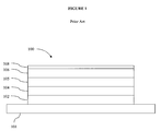
- typical thin film stack 100 for conventional magnetic recording media includes non-magnetic substrate base 101, seed layer 102, at least one underlayer 104, at least one interlayer 105, at least one magnetic data-storing layer 106, and lubricant layer 108.
- Data is stored on magnetic data-storing layer 106 in discrete domains which are magnetized to represent on or off states of bits of data.
- Grain refinement and grain-to-grain microstructural separation of magnetic materials are key in the construction of discrete magnetic domains with little cross-talk and a high signal-to-noise ratio (SNR).
- Various materials have been utilized as additives to cobalt (Co) based alloys, to improve this grain size reduction and separation, including chromium (Cr), boron (B) and tantalum (Ta). More recently work has begun to include dielectric materials, which effectuate the formation of "granular media," or materials with a granular microstructure in which nanoscale magnetic grains are encapsulated in an insulating matrix.
- dielectric materials which effectuate the formation of "granular media," or materials with a granular microstructure in which nanoscale magnetic grains are encapsulated in an insulating matrix.
- the present invention solves the foregoing problems by providing a sputter target material for reactively sputtering a granular medium with optimized grain size and grain-to-grain separation characteristics.
- the present invention is a sputter target composed of a ferromagnetic alloy having a base metal.
- the sputter target is further composed of X 1 , a metal having an atomic diameter of less than 0.266 nm and an oxidation potential greater than that of the base metal.
- the base metal of the ferromagnetic alloy of the sputter target is iron (Fe), Co, or any other ferromagnetic metal.
- the base metal is Co, and the ferromagnetic alloy is further composed of Ta, platinum (Pt), or PtCr.
- the base metal is Fe, and the ferromagnetic alloys is further composed of Ta or Pt.
- the features of the present invention include that X 1 is more quickly diffused to grain boundaries during sputtering and is more easily oxidized than other matrix materials. These features are further effectuated when X 1 has an atomic radius of less than 0.18 nm and an oxidation potential greater than -1.0 eV.
- the word “greater,” when referring to “greater oxidation potential,” indicates a more negative charge, measured in eV. For instance, an oxidation potential of -2.7 eV (Mg) is greater than that of -2.3 eV (Pm).
- X 1 is selected from the list of Al, Ba, Be, Ca, Cd, Ce, Cr, Cs, Dy, Er, Eu, Ga, Gd, Hf, Ho, K, La, Li, Mg, Mn, Na, Nb, Nd, Pm, Pr, Rb, Sc, Sm, Sr, Ta, Tb, Te, Th, Ti, V, Y, Zn, and Zr. Additionally, the sputter target material is composed of more than 0 atomic percent and less than fifteen atomic percent X 1 .
- the present invention is a method for manufacturing a magnetic recording medium.
- the method includes the step of reactively sputtering in the presence of oxygen a sputter target composed of a ferromagnetic alloy having a base metal, and X 2 , a metal having an atomic diameter of less than 0.266 nm and an oxidation potential greater than that of the base metal.
- the present invention is a magnetic recording medium having a substrate and a data-storing thin film layer formed over the substrate.
- the data-storing thin film layer is composed of a ferromagnetic alloy having a base metal, and an oxide of X 3 , a metal having an atomic diameter of less than 0.266 nm and an oxidation potential greater than that of the base metal.
- X 3 is selected from the list of Ba, Be, Ca, Cd, Ce, Cr, Cs, Dy, Er, Eu, Ga, Gd, Hf, Ho, K, La, Li, Mg, Mn, Na, Nb, Nd, Pm, Pr, Rb, Sc, Sm, Sr, Ta, Tb, Te, Th, Ti, V, Zn, and Zr.
- the present invention provides a granular medium with an insulating and anti-magnetic barrier to grain-on-grain interactions. If is another feature and advantage of the present invention to provide a magnetic recording medium with an improved signal-to-noise ratio.
- the present invention is an enhanced sputter target material which can be reactively sputtered to form magnetic data-storing thin films having granular media with optimized grain size and improved grain-to-grain separation.
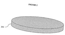
- FIG. 2 depicts a sputter target according to one embodiment of the present invention.
- Sputter target 200 is composed of a ferromagnetic alloy having a base metal, and X 1 , a metal having an atomic diameter of less than 0.266 nm and an oxidation potential greater than that of the base metal.
- the base metal of the ferromagnetic alloy of the sputter target is Fe, Co, or any other ferromagnetic metal.
- the base metal is Co, and the ferromagnetic alloy is further composed of Ta, Pt, or PtCr.
- the base metal is Fe, and the ferromagnetic alloys is further composed of Ta or Pt.
- the features of the present invention include that X 1 is more quickly diffused to grain boundaries during sputtering and is more easily oxidized than other matrix materials.
- the metals of Table 1 are to be considered as primary candidates for oxides in effective granular magnetic media. These features are further effectuated when X 1 is selected from the metals of Table 1 combining the greatest oxidation potential ( ⁇ -1.0 eV) and lowest atomic diameter ( ⁇ 0.18 nm).
- the sputter target material is composed of more than 0 atomic percent and less than fifteen atomic percent X 1 .
- Figures 3A, 3B and 3C depict the reactive sputtering of a sputter target to form a magnetic recording medium according to one embodiment of the present invention.
- Figure 3A depicts a macroscopic view of sputtering chamber 310.
- sputter target 200 is positioned in sputtering chamber 310, which is partially filled with both an inert gas and oxygen.
- Sputter target 200 is exposed to an electric field to excite the gas species to generate plasma 316.
- Ions within plasma 316 collide with a surface of sputter target 200 causing molecules to be emitted from the surface of sputter target 200.
- Some of the material which has been ejected off of sputter target 200 chemically reacts with oxygen in plasma 316 to form oxide molecules.
- a difference in voltage between sputter target 200 and substrate 312 causes the emitted molecules to form the desired thin film 314 on the surface of substrate 312.
- Figure 3B depicts a microscopic view of sputter target 200 during the above-described sputtering process.
- sputter target 200 is seen to be composed of molecules of ferromagnetic alloy 323 and X 2 molecules 324, where X 2 is a metal having an atomic diameter of less than 0.266 nm and an oxidation potential greater than that of the base metal.
- Surface 322 of sputter target 200 is bombarded by energetic ions 325 of the sputtering gas species of the plasma, such that molecules from sputter target 200 are ejected from surface 322.
- X 2 molecules 324 which are ejected react with oxygen molecules 326 in the plasma to form oxide groups 328, which, together with ejected ferromagnetic alloy molecules 327, are not in a state of thermodynamic equilibrium. Accordingly, these molecules will tend to condense back into the solid phase upon colliding with any surface in the sputtering chamber.
- Figure 3C depicts a microscopic view of substrate 312.
- Surface 332 of substrate 312 is coated with the ejected molecules from sputter target 200, which have condensed to form discrete grains 334 of ferromagnetic material and matrix 336 of oxide groups.
- Matrix 336 of oxide groups acts as an insulating and anti-magnetic barrier to interactions between grains 334 of ferromagnetic material, thereby improving the signal-to-noise ratio of the magnetic recording medium.
- Figures 3A, 3B, and 3C are not drawn to scale, and are merely simplified representations of the features of the present invention.
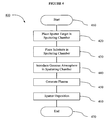
- flowchart 400 illustrates the steps of reactively sputtering a sputter target to deposit a thin film granular medium according to one embodiment of the present invention.
- a sputter target is provided, and is disposed inside of a sputtering chamber.
- the sputter target is composed of a ferromagnetic alloy having a base metal.
- the sputter target is further composed of X 2 , a metal having an atomic diameter of less than 0.266 nm and an oxidation potential greater than that of the base metal.
- the sputtering chamber is a vacuum chamber in which a reactive plasma can be contained, and in which both sputter targets and substrates can be disposed.
- a substrate is provided, and is disposed inside of the sputtering chamber.
- the substrate is positioned so as to accumulate a thin film during the sputtering process.
- the gaseous atmosphere comprising both a non-reactive gas species and oxygen, is introduced into the sputtering chamber to form a partial vacuum.
- step 450 the gas species in the sputtering chamber are excited to create a plasma.
- the gas species are excited by applying a voltage difference between the substrate and the sputter target.
- step 460 the material of the sputter target is deposited as a granular medium onto the substrate. This deposition is the result of the sputter target being bombarded by energetic ions of the sputtering gas species in the plasma, such that molecules from the sputter target are ejected from its surface. Molecules of X 2 which are ejected react with the oxygen molecules in the plasma to form oxide groups.
- Figure 5 depicts a thin film stack in which the magnetic data-storing layer has been reactively sputtered in the presence of oxygen by a sputter target composed of an enhanced composition according to one embodiment of the present invention.
- magnetic recording medium 500 includes non-magnetic substrate base 501, seed layer 502, at least one underlayer 504, at least one interlayer 505, data-storing thin film layer 506, and lubricant layer 508.
- the data-storing thin film layer 506 on magnetic recording medium 500 is composed of a ferromagnetic alloy, the ferromagnetic alloy having a base metal, and an oxide of X 3 , where X 3 is a metal having an atomic diameter of less than 0.266 nm and an oxidation potential greater than that of the base metal.
- magnetic recording medium 500 omits seed layer 502, underlayer 504, interlayer 505 and/or lubricant layer 508.
- features of the present invention include that X 3 is more quickly diffused to grain boundaries during sputtering and is more easily oxidized than other matrix materials.
- the metals of Table 2 are to be considered as primary candidates for oxides in effective granular magnetic media.
- the magnetic recording medium is composed of more than 0 atomic percent and less than fifteen atomic percent X 3 .
Abstract
Description
- The present invention relates to sputter targets and, more particularly, to improved sputter target materials which provide magnetic data-storing thin films with optimized grain size and grain-to-grain separation when reactively sputtered in the presence of oxygen.
- The process of sputtering is widely used in a variety of fields to provide thin film material deposition of a precisely controlled thickness with an atomically smooth surface, for example to coat semiconductors and/or to form films on surfaces of magnetic recording media. In the reactive sputtering process, a cathodic sputter target is positioned in a vacuum chamber partially filled with a chemically reactive gas atmosphere, and is exposed to an electric field to generate a plasma. Ions within this plasma collide with a surface of the sputter target causing the sputter target to emit atoms from the sputter target surface. Material which has been sputtered off of the target chemically reacts with the reactive species in the gas mixture to form a chemical compound which forms the desired film on the surface of the substrate.
- Conventional magnetic recording media typically comprise several thin film layers which are sequentially sputtered onto a substrate by multiple sputter targets. As illustrated in Figure 1, typical
thin film stack 100 for conventional magnetic recording media includesnon-magnetic substrate base 101,seed layer 102, at least oneunderlayer 104, at least oneinterlayer 105, at least one magnetic data-storing layer 106, andlubricant layer 108. Data is stored on magnetic data-storing layer 106 in discrete domains which are magnetized to represent on or off states of bits of data. - Grain refinement and grain-to-grain microstructural separation of magnetic materials are key in the construction of discrete magnetic domains with little cross-talk and a high signal-to-noise ratio (SNR). Various materials have been utilized as additives to cobalt (Co) based alloys, to improve this grain size reduction and separation, including chromium (Cr), boron (B) and tantalum (Ta). More recently work has begun to include dielectric materials, which effectuate the formation of "granular media," or materials with a granular microstructure in which nanoscale magnetic grains are encapsulated in an insulating matrix. Despite these enhancements, however, conventional materials have been unable to produce a data-storing thin film with sufficiently small grain size and sufficiently large grain-to-grain separation to keep up with the ever increasing demands of data storage.
- As the refinement of magnetic thin film media approaches the limits of magnetic dipole stability, it is increasingly desirable to develop materials with small grain sizes and sufficient grain-to-grain separation such that each grain is not magnetically influenced by neighboring grains in the medium. In particular, it is desirable to provide a sputter target material which can be reactively sputtered to form a granular medium with optimized grain size and grain-to-grain separation.
- The present invention solves the foregoing problems by providing a sputter target material for reactively sputtering a granular medium with optimized grain size and grain-to-grain separation characteristics.
- According to one aspect, the present invention is a sputter target composed of a ferromagnetic alloy having a base metal. The sputter target is further composed of X1, a metal having an atomic diameter of less than 0.266 nm and an oxidation potential greater than that of the base metal.
- The base metal of the ferromagnetic alloy of the sputter target is iron (Fe), Co, or any other ferromagnetic metal. In one arrangement, the base metal is Co, and the ferromagnetic alloy is further composed of Ta, platinum (Pt), or PtCr. In a second arrangement, the base metal is Fe, and the ferromagnetic alloys is further composed of Ta or Pt.
- Considering that it is a function of the oxide material in the magnetic recording medium to act as an insulating and anti-magnetic barrier to grain-on-grain interactions, the features of the present invention include that X1 is more quickly diffused to grain boundaries during sputtering and is more easily oxidized than other matrix materials. These features are further effectuated when X1 has an atomic radius of less than 0.18 nm and an oxidation potential greater than -1.0 eV.
- It is to be understood that the word "greater," when referring to "greater oxidation potential," indicates a more negative charge, measured in eV. For instance, an oxidation potential of -2.7 eV (Mg) is greater than that of -2.3 eV (Pm).
- X1 is selected from the list of Al, Ba, Be, Ca, Cd, Ce, Cr, Cs, Dy, Er, Eu, Ga, Gd, Hf, Ho, K, La, Li, Mg, Mn, Na, Nb, Nd, Pm, Pr, Rb, Sc, Sm, Sr, Ta, Tb, Te, Th, Ti, V, Y, Zn, and Zr. Additionally, the sputter target material is composed of more than 0 atomic percent and less than fifteen atomic percent X1.
- According to a second aspect, the present invention is a method for manufacturing a magnetic recording medium. The method includes the step of reactively sputtering in the presence of oxygen a sputter target composed of a ferromagnetic alloy having a base metal, and X2, a metal having an atomic diameter of less than 0.266 nm and an oxidation potential greater than that of the base metal.
- According to a third aspect, the present invention is a magnetic recording medium having a substrate and a data-storing thin film layer formed over the substrate. The data-storing thin film layer is composed of a ferromagnetic alloy having a base metal, and an oxide of X3, a metal having an atomic diameter of less than 0.266 nm and an oxidation potential greater than that of the base metal.
- X3 is selected from the list of Ba, Be, Ca, Cd, Ce, Cr, Cs, Dy, Er, Eu, Ga, Gd, Hf, Ho, K, La, Li, Mg, Mn, Na, Nb, Nd, Pm, Pr, Rb, Sc, Sm, Sr, Ta, Tb, Te, Th, Ti, V, Zn, and Zr.
- To its advantage, the present invention provides a granular medium with an insulating and anti-magnetic barrier to grain-on-grain interactions. If is another feature and advantage of the present invention to provide a magnetic recording medium with an improved signal-to-noise ratio.
- In the following description of the preferred embodiment, reference is made to the accompanying drawings that form a part thereof, and in which is shown by way of illustration a specific embodiment in which the invention may be practiced. It is to be understood that other embodiments may be utilized and changes may be made without departing from the scope of the present invention.
- Referring now to the drawings in which like reference numbers represent corresponding parts throughout:
- Figure 1 depicts a typical thin film stack for conventional magnetic recording media;
- Figure 2 depicts a sputter target according to one embodiment of the present invention;
- Figures 3A, 3B and 3C depict both macroscopic and microscopic views of the reactive sputtering of a sputter target to form a magnetic recording medium according to one embodiment of the present invention;
- Figure 4 is a flowchart depicting the process of reactively sputtering a sputter target according to one embodiment of the present invention; and
- Figure 5 depicts a thin film stack with an enhanced magnetic data-storing layer according to one embodiment of the present invention.
- The present invention is an enhanced sputter target material which can be reactively sputtered to form magnetic data-storing thin films having granular media with optimized grain size and improved grain-to-grain separation.
- Figure 2 depicts a sputter target according to one embodiment of the present invention.
Sputter target 200 is composed of a ferromagnetic alloy having a base metal, and X1, a metal having an atomic diameter of less than 0.266 nm and an oxidation potential greater than that of the base metal. - The base metal of the ferromagnetic alloy of the sputter target is Fe, Co, or any other ferromagnetic metal. In one arrangement, the base metal is Co, and the ferromagnetic alloy is further composed of Ta, Pt, or PtCr. In a second arrangement, the base metal is Fe, and the ferromagnetic alloys is further composed of Ta or Pt.
- It is a function of the oxide material in the magnetic recording medium to act as an insulating and anti-magnetic barrier to grain-on-grain interactions. As such, the features of the present invention include that X1 is more quickly diffused to grain boundaries during sputtering and is more easily oxidized than other matrix materials. In this regard, the metals of Table 1 are to be considered as primary candidates for oxides in effective granular magnetic media. These features are further effectuated when X1 is selected from the metals of Table 1 combining the greatest oxidation potential (< -1.0 eV) and lowest atomic diameter (< 0.18 nm).
TABLE 1 Metals sorted by Greatest Oxidation Potential Element Oxidation Potential* Atomic Radius† Ionic Radius† Li -3.0401 1.52 0.76 Cs -3.026 2.65 1.67 Rb -2.98 2.48 1.52 K -2.931 2.31 1.38 Ba -2.912 2.22 1.35 Sr -2.899 2.15 1.18 Ca -2.868 1.98 1.00 Na -2.71 1.86 1.02 Mg -2.7 1.61 0.72 La -2.379 1.88 1.03 Y -2.372 1.80 0.90 Pr -2.353 1.83 0.99 Ce -2.336 1.72 1.02 Er -2.331 1.76 0.89 Ho -2.33 1.77 0.90 Nd -2.323 1.82 0.98 Sm -2.304 1.80 0.96 Pm -2.3 1.81 0.97 Dy -2.295 1.77 0.91 Tb -2.28 1.78 0.92 Gd -2.279 1.80 0.94 Sc -2.077 1.64 0.75 Eu -1.991 2.04 0.95 Th -1.899 1.79 0.94 Be -1.847 1.14 0.27 Al -1.662 1.43 0.54 Ti -1.63 1.46 0.61 Hf -1.55 1.59 0.71 Zr -1.45 1.60 0.72 Mn -1.185 1.12 0.67 V -1.175 1.34 0.54 Te -1.143 1.60 0.56-0.97 Nb -1.099 1.46 0.64 Zn -0.7618 1.39 0.74 Cr -0.744 1.25 0.55 Ta -0.6 1.46 0.64 Ga -0.539 1.35 0.62 Cd -0.403 1.51 0.95 * in eV † in Ångstroms - Additionally, the sputter target material is composed of more than 0 atomic percent and less than fifteen atomic percent X1.
- Figures 3A, 3B and 3C depict the reactive sputtering of a sputter target to form a magnetic recording medium according to one embodiment of the present invention.
- In more detail, Figure 3A depicts a macroscopic view of
sputtering chamber 310. In the sputtering process,sputter target 200 is positioned insputtering chamber 310, which is partially filled with both an inert gas and oxygen.Sputter target 200 is exposed to an electric field to excite the gas species to generateplasma 316. Ions withinplasma 316 collide with a surface ofsputter target 200 causing molecules to be emitted from the surface ofsputter target 200. Some of the material which has been ejected off of sputter target 200 chemically reacts with oxygen inplasma 316 to form oxide molecules. A difference in voltage betweensputter target 200 andsubstrate 312 causes the emitted molecules to form the desiredthin film 314 on the surface ofsubstrate 312. - Figure 3B depicts a microscopic view of
sputter target 200 during the above-described sputtering process. At the molecular level,sputter target 200 is seen to be composed of molecules offerromagnetic alloy 323 and X2 molecules 324, where X2 is a metal having an atomic diameter of less than 0.266 nm and an oxidation potential greater than that of the base metal.Surface 322 ofsputter target 200 is bombarded byenergetic ions 325 of the sputtering gas species of the plasma, such that molecules fromsputter target 200 are ejected fromsurface 322. X2 molecules 324 which are ejected react withoxygen molecules 326 in the plasma to formoxide groups 328, which, together with ejectedferromagnetic alloy molecules 327, are not in a state of thermodynamic equilibrium. Accordingly, these molecules will tend to condense back into the solid phase upon colliding with any surface in the sputtering chamber. - Figure 3C depicts a microscopic view of
substrate 312.Surface 332 ofsubstrate 312 is coated with the ejected molecules fromsputter target 200, which have condensed to formdiscrete grains 334 of ferromagnetic material andmatrix 336 of oxide groups.Matrix 336 of oxide groups acts as an insulating and anti-magnetic barrier to interactions betweengrains 334 of ferromagnetic material, thereby improving the signal-to-noise ratio of the magnetic recording medium. - It is to be understood that Figures 3A, 3B, and 3C are not drawn to scale, and are merely simplified representations of the features of the present invention.
- In Figure 4,
flowchart 400 illustrates the steps of reactively sputtering a sputter target to deposit a thin film granular medium according to one embodiment of the present invention. - In
step 410, the process begins. Instep 420, a sputter target is provided, and is disposed inside of a sputtering chamber. The sputter target is composed of a ferromagnetic alloy having a base metal. The sputter target is further composed of X2, a metal having an atomic diameter of less than 0.266 nm and an oxidation potential greater than that of the base metal. The sputtering chamber is a vacuum chamber in which a reactive plasma can be contained, and in which both sputter targets and substrates can be disposed. - In
step 430, a substrate is provided, and is disposed inside of the sputtering chamber. The substrate is positioned so as to accumulate a thin film during the sputtering process. Instep 440, the gaseous atmosphere, comprising both a non-reactive gas species and oxygen, is introduced into the sputtering chamber to form a partial vacuum. - In
step 450, the gas species in the sputtering chamber are excited to create a plasma. The gas species are excited by applying a voltage difference between the substrate and the sputter target. Instep 460, the material of the sputter target is deposited as a granular medium onto the substrate. This deposition is the result of the sputter target being bombarded by energetic ions of the sputtering gas species in the plasma, such that molecules from the sputter target are ejected from its surface. Molecules of X2 which are ejected react with the oxygen molecules in the plasma to form oxide groups. Both these oxide groups and the ejected molecules of the ferromagnetic alloy, are not in a state of thermodynamic equilibrium, and will therefore tend to condense back into their solid phase upon colliding with any surface in the sputtering chamber. The substrate, being such a surface, therefore accumulates a thin film of the desired material during the sputtering process. Instep 470, the process terminates. - Figure 5 depicts a thin film stack in which the magnetic data-storing layer has been reactively sputtered in the presence of oxygen by a sputter target composed of an enhanced composition according to one embodiment of the present invention.
- In more detail,
magnetic recording medium 500 includes non-magnetic substrate base 501,seed layer 502, at least oneunderlayer 504, at least oneinterlayer 505, data-storingthin film layer 506, andlubricant layer 508. The data-storingthin film layer 506 onmagnetic recording medium 500 is composed of a ferromagnetic alloy, the ferromagnetic alloy having a base metal, and an oxide of X3, where X3 is a metal having an atomic diameter of less than 0.266 nm and an oxidation potential greater than that of the base metal. In an alternate arrangement,magnetic recording medium 500 omitsseed layer 502,underlayer 504,interlayer 505 and/orlubricant layer 508. - Considering that it is a function of the oxide material in the magnetic recording medium to act as an insulating and anti-magnetic barrier to grain-on-grain interactions, features of the present invention include that X3 is more quickly diffused to grain boundaries during sputtering and is more easily oxidized than other matrix materials. In this regard, the metals of Table 2 are to be considered as primary candidates for oxides in effective granular magnetic media. These features are further effectuated when X3 is selected from the metals combining the lowest atomic diameter (< 0.18 nm) and greatest oxidation potential (< -1.0 eV).
TABLE2 Metals sorted by Lowest Atomic Radius Element Oxidation Potential* Atomic Radius† Ionic Radius† Mn -1.185 1.12 0.67 Be -1.847 1.14 0.27 Cr -0.744 1.25 0.55 V -1.175 1.34 0.54 Ga -0.539 1.35 0.62 Zn -0.7618 1.39 0.74 Ti -1.63 1.46 0.61 Nb -1.099 1.46 0.64 Ta -0.6 1.46 0.64 Cd -0.403 1.51 0.95 Li -3.0401 1.52 0.76 Hf -1.55 1.59 0.71 Zr -1.45 1.60 0.72 Te -1.143 1.60 0.56-0.97 Mg -2.7 1.61 0.72 Sc -2.077 1.64 0.75 Ce -2.336 1.72 1.02 Er -2.331 1.76 0.89 Ho -2.33 1.77 0.90 Dy -2.295 1.77 0.91 Tb -2.28 1.78 0.92 Th -1.899 1.79 0.94 Sm -2.304 1.80 0.96 Gd -2.279 1.80 0.94 Pm -2.3 1.81 0.97 Nd -2.323 1.82 0.98 Pr -2.353 1.83 0.99 Na -2.71 1.86 1.02 La -2.379 1.88 1.03 Ca -2.868 1.98 1.00 Eu -1.991 2.04 0.95 Sr -2.899 2.15 1.18 Ba -2.912 2.22 1.35 K -2.931 2.31 1.38 Rb -2.98 2.48 1.52 Cs -3.026 2.65 1.67 * in eV † in Angstroms - Additionally, the magnetic recording medium is composed of more than 0 atomic percent and less than fifteen atomic percent X3.
- The invention has been described with particular illustrative embodiments. It is to be understood that the invention is not limited to the above-described embodiments and that various changes and modifications may be made by those of ordinary skill in the art without departing from the spirit and scope of the invention.
Claims (23)
- A sputter target comprised of:a ferromagnetic alloy, the ferromagnetic alloy comprising a base metal; andX1, wherein X1 is a metal having an atomic diameter of less than 0.266 nm and an oxidation potential greater than that of the base metal.
- A sputter target according to Claim 1, wherein said base metal is Co.
- A sputter target according to Claim 2, wherein said ferromagnetic alloy further comprises Ta.
- A sputter target according to Claim 2, wherein said ferromagnetic alloy further comprises Pt.
- A sputter target according to Claim 4, wherein said ferromagnetic alloy further comprises Cr.
- A sputter target according to Claim 1, wherein said base metal is Fe.
- A sputter target according to Claim 6, wherein said ferromagnetic alloy further comprises Ta.
- A sputter target according to Claim 6, wherein said ferromagnetic alloy further comprises Pt.
- A sputter target according to Claim 1, wherein X1 is a metal selected from the group consisting of Al, Ba, Be, Ca, Cd, Ce, Cr, Cs, Dy, Er, Eu, Ga, Gd, Hf, Ho, K, La, Li, Mg, Mn, Na, Nb, Nd, Pm, Pr, Rb, Sc, Sm, Sr, Ta, Tb, Te, Th, Ti, V, Y, Zn, and Zr.
- A sputter target according to Claim 1, wherein X1 has an atomic radius of less than 0.18 nm.
- A sputter target according to Claim 1, wherein the sputter target comprises more than 0 atomic percent and less than 15 atomic percent X1.
- A method for manufacturing a magnetic recording medium, comprising the step of:reactively sputtering a sputter target in an atmosphere comprising oxygen, wherein the sputter target is comprised ofa ferromagnetic alloy, the ferromagnetic alloy comprising a base metal; andX2, wherein X2 is a metal having an atomic diameter of less than 0.266 nm and an oxidation potential greater than that of the base metal.
- A magnetic recording medium sputtered on a substrate, comprising:a data-storing thin film layer formed over the substrate, wherein said data-storing thin film layer is comprised of:a ferromagnetic alloy, the ferromagnetic alloy comprising a base metal; andan oxide of X3, wherein X3 is a metal having an atomic diameter of less than 0.266 nm and an oxidation potential greater than that of the base metal.
- A medium according to Claim 13, wherein said base metal is Co.
- A medium according to Claim 14, wherein said ferromagnetic alloy further comprises Ta.
- A medium according to Claim 14, wherein said ferromagnetic alloy further comprises Pt.
- A medium according to Claim 16, wherein said ferromagnetic alloy further comprises Cr.
- A medium according to Claim 13, wherein said base metal is Fe.
- A medium according to Claim 18, wherein said ferromagnetic alloy further comprises Pt.
- A medium according to Claim 18, wherein said ferromagnetic alloy further comprises Ta.
- A medium according to Claim 13, wherein X3 is selected from the group consisting of Ba, Be, Ca, Cd, Ce, Cr, Cs, Dy, Er, Eu, Ga, Gd, Hf, Ho, K, La, Li, Mg, Mn, Na, Nb, Nd, Pm, Pr, Rb, Sc, Sm, Sr, Ta, Tb, Te, Th, Ti, V, Zn, and Zr.
- A medium according to Claim 13, wherein X3 has an atomic radius of less than 0.18 nm.
- A medium according to Claim 13, wherein the medium comprises more than 0 atomic percent and less than 15 atomic percent X3
Applications Claiming Priority (1)
| Application Number | Priority Date | Filing Date | Title |
|---|---|---|---|
| US10/930,794 US20060042938A1 (en) | 2004-09-01 | 2004-09-01 | Sputter target material for improved magnetic layer |
Publications (2)
| Publication Number | Publication Date |
|---|---|
| EP1637625A2 true EP1637625A2 (en) | 2006-03-22 |
| EP1637625A3 EP1637625A3 (en) | 2006-07-05 |
Family
ID=35478650
Family Applications (1)
| Application Number | Title | Priority Date | Filing Date |
|---|---|---|---|
| EP05254682A Withdrawn EP1637625A3 (en) | 2004-09-01 | 2005-07-27 | Target material. |
Country Status (8)
| Country | Link |
|---|---|
| US (1) | US20060042938A1 (en) |
| EP (1) | EP1637625A3 (en) |
| JP (1) | JP2006077323A (en) |
| KR (1) | KR20060050456A (en) |
| CN (1) | CN1743497A (en) |
| CZ (1) | CZ2005482A3 (en) |
| SG (1) | SG120312A1 (en) |
| TW (1) | TW200617192A (en) |
Families Citing this family (17)
| Publication number | Priority date | Publication date | Assignee | Title |
|---|---|---|---|---|
| US20060286414A1 (en) * | 2005-06-15 | 2006-12-21 | Heraeus, Inc. | Enhanced oxide-containing sputter target alloy compositions |
| US20060289294A1 (en) * | 2005-06-24 | 2006-12-28 | Heraeus, Inc. | Enhanced oxygen non-stoichiometry compensation for thin films |
| US7457153B1 (en) * | 2005-11-23 | 2008-11-25 | Samsung Electronics Co., Ltd. | Integrated circuit memory devices having magnetic memory cells therein that utilize dual-ferromagnetic data layers |
| JP4331182B2 (en) * | 2006-04-14 | 2009-09-16 | 山陽特殊製鋼株式会社 | Soft magnetic target material |
| US20070253103A1 (en) * | 2006-04-27 | 2007-11-01 | Heraeus, Inc. | Soft magnetic underlayer in magnetic media and soft magnetic alloy based sputter target |
| JP5037036B2 (en) * | 2006-05-02 | 2012-09-26 | 山陽特殊製鋼株式会社 | FeCo-based target material |
| JP4907259B2 (en) * | 2006-08-16 | 2012-03-28 | 山陽特殊製鋼株式会社 | FeCoB-based target material with Cr added |
| SG142249A1 (en) * | 2006-10-10 | 2008-05-28 | Hitachi Metals Ltd | Co-fe-zr based alloy sputtering target material and process for production thereof |
| JP2008121071A (en) * | 2006-11-13 | 2008-05-29 | Sanyo Special Steel Co Ltd | SOFT MAGNETIC FeCo BASED TARGET MATERIAL |
| JP5111835B2 (en) * | 2006-11-17 | 2013-01-09 | 山陽特殊製鋼株式会社 | (CoFe) ZrNb / Ta / Hf-based target material and method for producing the same |
| US20080170959A1 (en) * | 2007-01-11 | 2008-07-17 | Heraeus Incorporated | Full density Co-W magnetic sputter targets |
| JP5253781B2 (en) * | 2007-09-18 | 2013-07-31 | 山陽特殊製鋼株式会社 | Alloy target material for soft magnetic film layer in perpendicular magnetic recording media |
| JP5376250B2 (en) * | 2010-03-28 | 2013-12-25 | 三菱マテリアル株式会社 | Manufacturing method of sputtering target |
| CN105671498A (en) * | 2011-09-30 | 2016-06-15 | 吉坤日矿日石金属株式会社 | Fe-Al based alloy sputtering target |
| CN103667997A (en) * | 2013-11-08 | 2014-03-26 | 张超 | Refractory steel material for pump valves and preparation method thereof |
| CN106521345A (en) * | 2016-10-18 | 2017-03-22 | 河池学院 | Low-temperature-resistant material for medical robot |
| JP7462636B2 (en) * | 2019-07-18 | 2024-04-05 | 田中貴金属工業株式会社 | Sputtering targets for magnetic recording media |
Citations (2)
| Publication number | Priority date | Publication date | Assignee | Title |
|---|---|---|---|---|
| US4992095A (en) * | 1988-10-26 | 1991-02-12 | Sumitomo Metal Mining Company, Ltd. | Alloy target used for manufacturing magneto-optical recording medium |
| EP1607940A2 (en) * | 2004-06-15 | 2005-12-21 | Heraeus, Inc. | Enhanced sputter target alloy compositions |
Family Cites Families (95)
| Publication number | Priority date | Publication date | Assignee | Title |
|---|---|---|---|---|
| US3147112A (en) * | 1961-01-19 | 1964-09-01 | Du Pont | Ferromagnetic mn-ga alloy and method of production |
| JPS5789450A (en) * | 1980-11-21 | 1982-06-03 | Matsushita Electric Ind Co Ltd | Amorphous magnetic alloy |
| US4868070A (en) * | 1984-11-29 | 1989-09-19 | Fuji Photo Film Co., Ltd. | Vertical magnetization type recording medium and manufacturing method therefor |
| US4994321A (en) * | 1986-01-24 | 1991-02-19 | Fuji Photo Film Co., Ltd. | Perpendicular magnetic recording medium and the method for preparing the same |
| DE3707522A1 (en) * | 1986-03-12 | 1987-09-24 | Matsushita Electric Ind Co Ltd | MAGNETIC NITRIDE FILM |
| JP2513205B2 (en) * | 1987-02-04 | 1996-07-03 | ソニー株式会社 | Composite magnetic head |
| JP2524514B2 (en) * | 1987-09-21 | 1996-08-14 | 日立マクセル株式会社 | Magnetic recording media |
| US5164025A (en) * | 1988-11-02 | 1992-11-17 | Alps Electric Co., Ltd. | Soft magnetic alloy film and a magnetic head using such soft a magnetic alloy film |
| US5772797A (en) * | 1989-01-26 | 1998-06-30 | Fuji Photo Film Co., Ltd. | Soft magnetic thin film, method for preparing same and magnetic head |
| KR920003999B1 (en) * | 1989-03-08 | 1992-05-21 | 알프스 덴기 가부시기가이샤 | Molted membrane of soft magnetics |
| JPH02292721A (en) * | 1989-05-02 | 1990-12-04 | Tdk Corp | Magnetic disk |
| JPH03116409A (en) * | 1989-09-29 | 1991-05-17 | Canon Electron Inc | Magnetic head |
| JP2635422B2 (en) * | 1989-10-17 | 1997-07-30 | アルプス電気株式会社 | Magnetic head |
| JPH03157801A (en) * | 1989-11-16 | 1991-07-05 | Tdk Corp | Magnetic recording and reproducing method |
| CA2030446C (en) * | 1989-11-22 | 2001-01-23 | Yoshihito Yoshizawa | Magnetic alloy with ultrafine crystal grains and method of producing same |
| US5182693A (en) * | 1989-12-29 | 1993-01-26 | Tdk Corporation | Magnetic disk |
| JPH0785452B2 (en) * | 1990-04-20 | 1995-09-13 | 日本電気株式会社 | Magnetic film and method for manufacturing the same |
| JP2789806B2 (en) * | 1990-09-28 | 1998-08-27 | 松下電器産業株式会社 | Fabrication method of soft magnetic nitride alloy film |
| JPH04214205A (en) * | 1990-12-12 | 1992-08-05 | Fuji Electric Co Ltd | Thin-film magnetic head and its production |
| WO1993011531A1 (en) * | 1991-12-02 | 1993-06-10 | Nikko Kyodo Company, Limited | Thin film magnetic head |
| JPH05304026A (en) * | 1992-02-29 | 1993-11-16 | Sony Corp | Soft magnetic thin film and magnetic head using the same |
| JP2586367B2 (en) * | 1992-04-15 | 1997-02-26 | 日本電気株式会社 | Soft magnetic material, method of manufacturing the same, and magnetic head |
| JP3279399B2 (en) * | 1992-09-14 | 2002-04-30 | アルプス電気株式会社 | Method for producing Fe-based soft magnetic alloy |
| US5931032A (en) * | 1998-04-16 | 1999-08-03 | Gregory; Edwin H. | Cutter and blow resistant lock |
| JP2961034B2 (en) * | 1993-09-16 | 1999-10-12 | アルプス電気株式会社 | Magnetic head |
| US5846648A (en) * | 1994-01-28 | 1998-12-08 | Komag, Inc. | Magnetic alloy having a structured nucleation layer and method for manufacturing same |
| JPH07268610A (en) * | 1994-03-28 | 1995-10-17 | Alps Electric Co Ltd | Soft magnetic alloy thin film |
| US5620574A (en) * | 1994-08-26 | 1997-04-15 | Stormedia, Inc. | Method of fabricating sputter induced, micro-texturing of thin film, magnetic disc media |
| US5800931A (en) * | 1994-09-29 | 1998-09-01 | Carnegie Mellon University | Magnetic recording medium with a MgO sputter deposited seed layer |
| JPH0917632A (en) * | 1995-06-28 | 1997-01-17 | Sony Corp | Soft magnetic film and magnetic head using the same |
| US5780175A (en) * | 1996-02-02 | 1998-07-14 | Lucent Technologies Inc. | Articles comprising magnetically soft thin films and methods for making such articles |
| US5909345A (en) * | 1996-02-22 | 1999-06-01 | Matsushita Electric Industrial Co., Ltd. | Magnetoresistive device and magnetoresistive head |
| TW367493B (en) * | 1996-04-30 | 1999-08-21 | Toshiba Corp | Reluctance component |
| US6698172B2 (en) * | 1996-07-27 | 2004-03-02 | Ferris Industries, Inc. | Lawn mower suspension assembly |
| US6690553B2 (en) * | 1996-08-26 | 2004-02-10 | Kabushiki Kaisha Toshiba | Magnetoresistance effect device, magnetic head therewith, magnetic recording/reproducing head, and magnetic storing apparatus |
| KR100265986B1 (en) * | 1997-01-31 | 2000-09-15 | 가타오카 마사타카 | Composite-typed thin film magnetic head and method for manufacturing the same |
| JPH10340431A (en) * | 1997-06-04 | 1998-12-22 | Fujitsu Ltd | Magneto-resistance effect type head and magnetic recording/reproducing device |
| JP3544293B2 (en) * | 1997-07-31 | 2004-07-21 | 株式会社日鉱マテリアルズ | Mn alloy material for magnetic material, Mn alloy sputtering target and magnetic thin film |
| JP3182399B2 (en) * | 1997-09-17 | 2001-07-03 | 株式会社東芝 | Soft magnetic alloy film and manufacturing method thereof, magnetic head, and magnetic disk |
| US6042897A (en) * | 1997-11-17 | 2000-03-28 | Alps Electric Co., Ltd. | Combination read/write thin film magnetic head and its manufacturing method |
| JPH11175920A (en) * | 1997-12-05 | 1999-07-02 | Nec Corp | Magneto-resistance effect type combined head and its manufacture |
| JP3263018B2 (en) * | 1997-12-09 | 2002-03-04 | アルプス電気株式会社 | Magnetoresistive element and method of manufacturing the same |
| US6232775B1 (en) * | 1997-12-26 | 2001-05-15 | Alps Electric Co., Ltd | Magneto-impedance element, and azimuth sensor, autocanceler and magnetic head using the same |
| US5996213A (en) * | 1998-01-30 | 1999-12-07 | Read-Rite Corporation | Thin film MR head and method of making wherein pole trim takes place at the wafer level |
| US6228515B1 (en) * | 1998-02-17 | 2001-05-08 | Korea Institute Of Science And Technology | Underlayer for use in a high density magnetic recording media |
| KR100270605B1 (en) * | 1998-04-23 | 2000-12-01 | 박호군 | Fe based soft magnetic film alloys and their manufacturing method |
| JP2000187808A (en) * | 1998-12-22 | 2000-07-04 | Alps Electric Co Ltd | Soft magnetic film and its production and thin film magnetic head using this soft magnetic film |
| US6524491B1 (en) * | 1999-04-26 | 2003-02-25 | Headway Technologies, Inc. | Double plate-up process for fabrication of composite magnetoresistive shared poles |
| JP2000322726A (en) * | 1999-05-12 | 2000-11-24 | Fuji Electric Co Ltd | Magnetic recording medium, manufacture of the same and magnetic recording device |
| US6331364B1 (en) * | 1999-07-09 | 2001-12-18 | International Business Machines Corporation | Patterned magnetic recording media containing chemically-ordered FePt of CoPt |
| US6718543B2 (en) * | 1999-11-08 | 2004-04-06 | Hewlett-Packard Development Company, L.P. | Method and apparatus for optimization of the performance of an application program in a computer system while preserving the system behavior |
| JP3731640B2 (en) * | 1999-11-26 | 2006-01-05 | 株式会社日立グローバルストレージテクノロジーズ | Perpendicular magnetic recording medium and magnetic storage device |
| US6620531B1 (en) * | 1999-12-20 | 2003-09-16 | Seagate Technology Llc | Magnetic recording media with oxidized seedlayer for reduced grain size and reduced grain size distribution |
| US6524724B1 (en) * | 2000-02-11 | 2003-02-25 | Seagate Technology Llc | Control of magnetic film grain structure by modifying Ni-P plating of the substrate |
| JP4207140B2 (en) * | 2000-04-06 | 2009-01-14 | 富士電機デバイステクノロジー株式会社 | Perpendicular magnetic recording medium and manufacturing method thereof |
| JP3665261B2 (en) * | 2000-09-01 | 2005-06-29 | 株式会社日立製作所 | Perpendicular magnetic recording medium and magnetic storage device |
| US6667118B1 (en) * | 2000-09-05 | 2003-12-23 | Seagate Technology Llc | Texture-induced magnetic anisotropy of soft underlayers for perpendicular recording media |
| US7029772B2 (en) * | 2000-09-11 | 2006-04-18 | Showa Denko Kabushiki Kaisha | Magnetic recording medium, production process thereof, and magnetic recording and reproducing apparatus |
| US6821653B2 (en) * | 2000-09-12 | 2004-11-23 | Showa Denko Kabushiki Kaisha | Magnetic recording medium, process for producing the same, and magnetic recording and reproducing apparatus |
| JP2002100030A (en) * | 2000-09-21 | 2002-04-05 | Toshiba Corp | Perpendicular magnetic recording medium |
| JP2002100018A (en) * | 2000-09-25 | 2002-04-05 | Fujitsu Ltd | Magnetic recording medium, method for producing the same, and magnetic storage device |
| US20020076579A1 (en) * | 2000-10-27 | 2002-06-20 | Showa Denko Kabushiki Kaisha | Magnetic recording medium, production process thereof, magnetic recording and reproducing apparatus, and medium substrate |
| US20020106297A1 (en) * | 2000-12-01 | 2002-08-08 | Hitachi Metals, Ltd. | Co-base target and method of producing the same |
| JP3629431B2 (en) * | 2001-01-15 | 2005-03-16 | アルプス電気株式会社 | Method for manufacturing soft magnetic film and method for manufacturing thin film magnetic head |
| JP3730518B2 (en) * | 2001-01-19 | 2006-01-05 | 株式会社東芝 | Magnetic recording medium |
| US6777066B1 (en) * | 2001-03-07 | 2004-08-17 | Seagate Technology Llc | Perpendicular magnetic recording media with improved interlayer |
| SG115476A1 (en) * | 2001-05-23 | 2005-10-28 | Showa Denko Kk | Magnetic recording medium, method of manufacturing therefor and magnetic replay apparatus |
| US6682826B2 (en) * | 2001-08-01 | 2004-01-27 | Showa Denko K.K. | Magnetic recording medium, method of manufacturing therefor, and magnetic read/write apparatus |
| US6692619B1 (en) * | 2001-08-14 | 2004-02-17 | Seagate Technology Llc | Sputtering target and method for making composite soft magnetic films |
| US6723458B2 (en) * | 2001-08-17 | 2004-04-20 | Showa Denko K.K. | Magnetic recording medium, method of manufacture therefor, and magnetic read/write apparatus |
| US6818331B2 (en) * | 2001-08-28 | 2004-11-16 | Showa Denko Kabushiki Kaisha | Magnetic recording medium, production process thereof, and magnetic recording and reproducing apparatus |
| JP4626840B2 (en) * | 2001-08-31 | 2011-02-09 | 富士電機デバイステクノロジー株式会社 | Perpendicular magnetic recording medium and manufacturing method thereof |
| JP2003099911A (en) * | 2001-09-26 | 2003-04-04 | Fujitsu Ltd | Magnetic recording medium and its manufacturing method |
| US6926977B2 (en) * | 2001-10-22 | 2005-08-09 | Showa Denko Kabushiki Kaisha | Magnetic recording medium, production process thereof, and magnetic recording and reproducing apparatus |
| US7138196B2 (en) * | 2001-11-09 | 2006-11-21 | Maxtor Corporation | Layered thin-film media for perpendicular magnetic recording |
| US7842409B2 (en) * | 2001-11-30 | 2010-11-30 | Seagate Technology Llc | Anti-ferromagnetically coupled perpendicular magnetic recording media with oxide |
| JP4019703B2 (en) * | 2001-12-07 | 2007-12-12 | 富士電機デバイステクノロジー株式会社 | Perpendicular magnetic recording medium and manufacturing method thereof |
| JP4011355B2 (en) * | 2002-02-04 | 2007-11-21 | 富士通株式会社 | Soft magnetic film and thin film magnetic head |
| US7186471B2 (en) * | 2002-02-28 | 2007-03-06 | Seagate Technology Llc | Chemically ordered, cobalt-three platinum alloys for magnetic recording |
| JP4270797B2 (en) * | 2002-03-12 | 2009-06-03 | Tdk株式会社 | Magnetic detection element |
| US6972157B2 (en) * | 2002-03-26 | 2005-12-06 | Waseda University | Magnetic recording medium, production process thereof, and magnetic recording and reproducing apparatus |
| US20030228238A1 (en) * | 2002-06-07 | 2003-12-11 | Wenjun Zhang | High-PTF sputtering targets and method of manufacturing |
| US6912106B1 (en) * | 2002-08-06 | 2005-06-28 | Western Digital (Fremont), Inc. | Writer with a hot seed zero throat and substantially flat top pole |
| JP2004079058A (en) * | 2002-08-14 | 2004-03-11 | Toshiba Corp | Perpendicular magnetic recording medium and magnetic recording/reproducing device |
| JP4047114B2 (en) * | 2002-09-13 | 2008-02-13 | アルプス電気株式会社 | Thin film magnetic head |
| CN1723292A (en) * | 2002-12-09 | 2006-01-18 | 霍尼韦尔国际公司 | High purity nickel/vanadium sputtering components, and methods of making sputtering components |
| US20040191578A1 (en) * | 2003-03-24 | 2004-09-30 | Jingsheng Chen | Method of fabricating L10 ordered fePt or FePtX thin film with (001) orientation |
| JP4169663B2 (en) * | 2003-07-25 | 2008-10-22 | Hoya株式会社 | Perpendicular magnetic recording medium |
| US7033685B2 (en) * | 2003-10-07 | 2006-04-25 | Seagate Technology Llc | High coercivity perpendicular magnetic recording media on polymer substrates |
| KR100590530B1 (en) * | 2003-12-10 | 2006-06-15 | 삼성전자주식회사 | Perpendicular magnetic recording media |
| US7297422B2 (en) * | 2003-12-19 | 2007-11-20 | Seagate Technology Llc | Method for sputtering magnetic recording media |
| US7837836B2 (en) * | 2004-02-12 | 2010-11-23 | Seagate Technology Llc | Method and apparatus for multi-stage sputter deposition of uniform thickness layers |
| US20050181239A1 (en) * | 2004-02-12 | 2005-08-18 | Seagate Technology Llc | Granular magnetic recording media with improved corrosion resistance by pre-carbon overcoat ion etching |
| US7310202B2 (en) * | 2004-03-25 | 2007-12-18 | Seagate Technology Llc | Magnetic recording head with clad coil |
| JP2005276365A (en) * | 2004-03-25 | 2005-10-06 | Toshiba Corp | Granular thin film, vertical magnetic recording medium, and magnetic recording/reproducing device |
-
2004
- 2004-09-01 US US10/930,794 patent/US20060042938A1/en not_active Abandoned
-
2005
- 2005-07-25 CZ CZ20050482A patent/CZ2005482A3/en unknown
- 2005-07-26 JP JP2005215408A patent/JP2006077323A/en not_active Withdrawn
- 2005-07-27 EP EP05254682A patent/EP1637625A3/en not_active Withdrawn
- 2005-08-01 TW TW094125992A patent/TW200617192A/en unknown
- 2005-08-12 KR KR1020050074463A patent/KR20060050456A/en active IP Right Grant
- 2005-09-01 SG SG200505612A patent/SG120312A1/en unknown
- 2005-09-01 CN CNA2005100978763A patent/CN1743497A/en active Pending
Patent Citations (2)
| Publication number | Priority date | Publication date | Assignee | Title |
|---|---|---|---|---|
| US4992095A (en) * | 1988-10-26 | 1991-02-12 | Sumitomo Metal Mining Company, Ltd. | Alloy target used for manufacturing magneto-optical recording medium |
| EP1607940A2 (en) * | 2004-06-15 | 2005-12-21 | Heraeus, Inc. | Enhanced sputter target alloy compositions |
Also Published As
| Publication number | Publication date |
|---|---|
| CN1743497A (en) | 2006-03-08 |
| SG120312A1 (en) | 2006-03-28 |
| JP2006077323A (en) | 2006-03-23 |
| KR20060050456A (en) | 2006-05-19 |
| TW200617192A (en) | 2006-06-01 |
| CZ2005482A3 (en) | 2006-11-15 |
| US20060042938A1 (en) | 2006-03-02 |
| EP1637625A3 (en) | 2006-07-05 |
Similar Documents
| Publication | Publication Date | Title |
|---|---|---|
| EP1637625A2 (en) | Target material. | |
| EP1736968B1 (en) | Enhanced oxygen non-stoichiometry compensation for thin films | |
| US20060234091A1 (en) | Enhanced multi-component oxide-containing sputter target alloy compositions | |
| US7494617B2 (en) | Enhanced formulation of cobalt alloy matrix compositions | |
| US20080057350A1 (en) | Magnetic media and sputter targets with compositions of high anisotropy alloys and oxide compounds | |
| KR100776383B1 (en) | Enhanced sputter target alloy compositions | |
| EP1734513A1 (en) | Enhanced oxide-containing sputter target alloy compositions | |
| US20020098383A1 (en) | Magnetic recording medium | |
| US20040084298A1 (en) | Fabrication of nanocomposite thin films for high density magnetic recording media | |
| US7771570B2 (en) | Method and apparatus for depositing a magnetoresistive multilayer film | |
| KR100830619B1 (en) | Enhanced sputter target alloy compositions | |
| Lee et al. | CrMn underlayers for CoCrPt thin film media | |
| US6667116B1 (en) | Magnetic recording media, the manufacturing method for the same, and magnetic recording device | |
| EP1211674A1 (en) | Magnetic recording medium and production method therefor and magnetic recording device | |
| KR20150010520A (en) | Hard magnetic exchange coupled composite structure and perpendicular magnetic recording medium comprising the same | |
| US20050249981A1 (en) | Grain structure for magnetic recording media | |
| JPH09306733A (en) | Magnetoresistive effect film | |
| JPH1166533A (en) | Magnetic recording medium | |
| JPH05143953A (en) | Magnetic recording medium | |
| JPH08277445A (en) | Magnetoresistance effect material and its production | |
| JPH02121113A (en) | Magnetic disk |
Legal Events
| Date | Code | Title | Description |
|---|---|---|---|
| PUAI | Public reference made under article 153(3) epc to a published international application that has entered the european phase |
Free format text: ORIGINAL CODE: 0009012 |
|
| AK | Designated contracting states |
Kind code of ref document: A2 Designated state(s): AT BE BG CH CY CZ DE DK EE ES FI FR GB GR HU IE IS IT LI LT LU LV MC NL PL PT RO SE SI SK TR |
|
| AX | Request for extension of the european patent |
Extension state: AL BA HR MK YU |
|
| PUAL | Search report despatched |
Free format text: ORIGINAL CODE: 0009013 |
|
| REG | Reference to a national code |
Ref country code: HK Ref legal event code: DE Ref document number: 1082527 Country of ref document: HK |
|
| RIC1 | Information provided on ipc code assigned before grant |
Ipc: G11B 5/851 20060101ALN20060522BHEP Ipc: G11B 5/73 20060101ALI20060522BHEP Ipc: C23C 14/34 20060101AFI20060103BHEP |
|
| AK | Designated contracting states |
Kind code of ref document: A3 Designated state(s): AT BE BG CH CY CZ DE DK EE ES FI FR GB GR HU IE IS IT LI LT LU LV MC NL PL PT RO SE SI SK TR |
|
| AX | Request for extension of the european patent |
Extension state: AL BA HR MK YU |
|
| 17P | Request for examination filed |
Effective date: 20060825 |
|
| 17Q | First examination report despatched |
Effective date: 20070125 |
|
| AKX | Designation fees paid |
Designated state(s): DE FR GB |
|
| STAA | Information on the status of an ep patent application or granted ep patent |
Free format text: STATUS: THE APPLICATION IS DEEMED TO BE WITHDRAWN |
|
| 18D | Application deemed to be withdrawn |
Effective date: 20081008 |
|
| REG | Reference to a national code |
Ref country code: HK Ref legal event code: WD Ref document number: 1082527 Country of ref document: HK |