EP1596305A1 - Interrupt handling system - Google Patents
Interrupt handling system Download PDFInfo
- Publication number
- EP1596305A1 EP1596305A1 EP04252720A EP04252720A EP1596305A1 EP 1596305 A1 EP1596305 A1 EP 1596305A1 EP 04252720 A EP04252720 A EP 04252720A EP 04252720 A EP04252720 A EP 04252720A EP 1596305 A1 EP1596305 A1 EP 1596305A1
- Authority
- EP
- European Patent Office
- Prior art keywords
- interrupt
- processor
- active level
- input
- handling system
- Prior art date
- Legal status (The legal status is an assumption and is not a legal conclusion. Google has not performed a legal analysis and makes no representation as to the accuracy of the status listed.)
- Granted
Links
Images


Classifications
-
- G—PHYSICS
- G06—COMPUTING OR CALCULATING; COUNTING
- G06F—ELECTRIC DIGITAL DATA PROCESSING
- G06F13/00—Interconnection of, or transfer of information or other signals between, memories, input/output devices or central processing units
- G06F13/14—Handling requests for interconnection or transfer
- G06F13/20—Handling requests for interconnection or transfer for access to input/output bus
- G06F13/24—Handling requests for interconnection or transfer for access to input/output bus using interrupt
Definitions
- the present invention relates to an interrupt handling system, particularly for processor generated interrupts.
- a set top box is one example of a system on a chip. Where multiple processors form part of the system, they need to be able to communicate with one another and this is done by way of interprocessor interrupts.
- interprocessor interrupts are managed by a mailbox which receives a message from one processor that it wishes to interrupt another on-chip processor, and generates the interrupt accordingly.
- the mailbox includes enable/clear logic and optionally a status register for dealing with these interprocessor interrupts.
- the mailbox has a dedicated interface to a system bus to which the processors are connected and only deals with the interprocessor interrupts.
- Interprocessor interrupts may include, in addition to the interrupt itself, extra information, for example the location of data associated with the interrupt.
- the mailbox includes memory locations, for example in the form of registers, which allow this information to be held and accessed by the processor being interrupted.
- an on-chip system generally includes an interrupt level controller which handles other interrupts of the system, for example external interrupts which are received from the chip pads and internal interrupts which are received from the other on-chip active devices.
- An interrupt level controller has an array of inputs associated with the different sources of interrupts and includes enable/clear logic, routing logic and detection logic for detecting interrupts.
- An interrupt level controller may include status registers which hold the status of interrupts, but it does not include any way of handling additional information of a type which might be required with interprocessor interrupts. However, the interrupt level controller does allow the mapping of different interrupts to different processors, switching them on and off, clearing them and thus provides a great deal of flexibility.
- Interrupt level controllers are known which have detection circuits associated with the respective interrupt inputs, the detection circuit being configurable to detect different types of interrupt, for example high level, low level, rising edge, falling edge, Edge or no edge (i.e. never detects).
- an interrupt handling system for processor generated interrupts comprising: at least one input arranged to provide a predetermined active level; a detection circuit associated with the at least one input and selectively configurable to detect either the active level or an inactive level; control circuitry responsive to an interrupt request message from a processor to configure the detection circuit to detect the active level; and enable logic responsive to detection of the active level by the detection circuit to generate an interrupt.
- the predetermined active level can be high or low and can be provided by tying an input pin to a high or low voltage accordingly.
- the invention also provides an integrated circuit which includes such an interrupt handling system, a set of processors interconnected by a system bus and a shared memory resource connected to the system bus.
- the invention also provides in another aspect a method of generating interrupts comprising: generating from a first processor an interrupt request message; configuring detection circuitry associated with at least one interrupt input which is arranged to provide a predetermined active level so that said detection circuit is configured to detect the active level; and generating an interrupt to the second processor responsive to the detection circuit detecting the active level.
- the invention further provides a consumer electronic device in the form of a Set Top Box or DVD Read and/or Write device utilising the above defined system or method.
- FIG. 1 is a schematic block diagram of the relevant components of an integrated circuit with multiple processors to show the schema for handling interrupts.
- On-chip circuitry comprises a first processor CPU1, a second processor CPU2 and a mailbox 2 which are connected to a system bus 4.
- An interrupt level controller 6 is also connected to the system bus via communication path 8 which allows the interrupt level controller 6 to be configured as will be explained later.
- the interrupt level controller 6 is connected to the first processor CPU1 via a first interrupt path 10 for passing interrupts to that processor.
- the first processor CPU1 is sometimes referred to herein as the remote processor.
- the interrupt level controller 6 also has a second interrupt path 12 connected to the second processor CPU2, which is sometimes referred to herein as the local processor.
- the interrupt level controller 6 has a first set of inputs 14 for receiving external interrupt requests 16 which come, for example, from pads 18 of the integrated circuit, and a second set of inputs 20 for receiving internal interrupt requests 22 which come from other devices on the same chip.
- the interrupt level controller has an input for receiving mailbox interrupt requests.
- the mailbox 2 has an output 24 which outputs interrupt requests either to the interrupt level controller via input 21 or to each of the first and second processors directly as indicated by the dotted path 26.
- each input in the set of external request inputs 14 is associated with detection logic which is configurable to detect one of the different kinds of interrupts, that is high level, low level, rising edge, falling edge, any edge or no edge.
- the detection circuit at each input is independently configurable via the communication path 8 under the control of one of the processors CPU1, CPU2.
- the detection circuits are configured, for example, at the start of each application so that an interrupt arriving at any particular input is detected in the proper manner.
- the interrupt level controller 6 also includes enable/clear logic and routing logic which will be described in more detail later in the context of an embodiment of the invention.
- Each processor is equipped with an interrupt controller, which is shown by reference numeral 28 for the first processor CPU1.
- a similar interrupt controller is present in the second processor CPU2 although it is not shown in Figure 1.
- These interrupt controllers handle interrupts in a known manner.
- the interrupt level controller reads an interrupt request on input 21 from the mailbox 2 and if enabled and routed, generates an interrupt along path 10, 12 to the appropriate processor CPU1, CPU2.
- the mailbox 2 contains a status register which can be read by the processor being interrupted to determine the status of the interrupt, i.e. whether it is still pending or whether it is cleared.
- the interrupt controller 28 reads the interrupt request and routes the interrupt over path 10 to the first processor CPU1.
- the first processor CPU1 then reads the mailbox 2 or the interrupt level controller 6 to clear the interrupt request when it has been dealt with.
- the mailbox 2 optionally includes memory for holding the additional information which can be sent with the interrupt request message. This additional information can be accessed by the interrupted processor over the system bus 4.
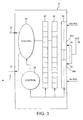
- Figure 2 illustrates a schematic block diagram in which the processors can generate interrupts for each other without the use of a mailbox.
- the interrupt level controller is denoted 6' to distinguish it from the interrupt level controller 6 of Figure 1, though the functionality is the same.
- the interrupt level controller 6' includes a set of additional inputs, two of which 30, 32 are shown in Figure 2. The difference lies in the way these inputs are handled. While only two additional inputs are shown, there is at least one separate additional input for each processor in the system. There might, for example, be more than one additional input associated with each processor to indicate interrupts of different priority levels.
- the additional inputs 30, 32 are tied to a common active level. In this example input 30 is associated with CPU1 and input 32 with CPU2.
- the interrupt level controller 6' includes detect logic 36 which has detect circuits associated with the inputs and including circuits 36a, 36b for each of the additional inputs 30, 32.
- the interrupt level controller 6' includes control logic 38 which configures the detect circuits 36 under the control of one of the processors CPU1, CPU2 via the communication path 8.
- the interrupt level controller 6' also includes enable/clear registers 40, routing logic 41 and a set of status registers 42, one associated with each input.
- the system additionally includes shared memory 44 connected to the system bus 4.
- the system operates as follows to deal with interprocessor interrupts.
- the detection circuits 36 are each configured to detect the kind of interrupt expected at their associated input, as already described with reference to Figure 1.
- the detection circuits 36a, 36b associated with each of the additional inputs 30, 32 are set to detect a zero or low level. That is, in normal operation no interrupt will be detected by the detection circuits 36a, 36b associated with the additional inputs.
- CPU1 When one of the processors CPU1, CPU2 wishes to generate an interrupt to the other processor, it first generates a message which is transmitted along communication path 8 to the control logic 38 of the interrupt level controller 6' which reconfigures the detection circuit associated with the input for the processor which is to be interrupted. Say, for example, in the case of the first processor CPU1 wishing to generate an interrupt to the second processor CPU2, a message is sent by the path 8 to the control logic 38 to reconfigure the detection circuit 36b so that it now detects a one (or high), rather than a zero. As that input is permanently tied to active high, it will immediately respond as though an interrupt has been received at that input.
- the status register in the block 42 associated with that input is set to a status of interrupt pending, and the associated enable/clear register 40 is set to generate an interrupt along path 12 via the routing logic 41.
- the routing logic 41 maps interrupts received at the set of inputs 14, 20, 30, 32 to the appropriate processor based on the source of the interrupts.
- the routing logic is configured when the system is set up and the interrupts are first determined.
- the routing logic is also sometimes referred to as mapping logic.
- the routing logic 42 determines that the interrupt was detected at the additional input 32 which is an interrupt source intended for the second processor CPU2. Therefore, the interrupt is generated along path 12. If the interrupt was associated with additional information, the first processor accesses the shared memory 44 and stores that additional information in a predetermined location.
- the shared memory 44 is a resource which is already available on the chip, and which in this embodiment has a set of predetermined locations associated with each of the processors CPU1, CPU2 for holding information about the interrupt, for example its reason and priority.
Landscapes
- Engineering & Computer Science (AREA)
- Theoretical Computer Science (AREA)
- Physics & Mathematics (AREA)
- General Engineering & Computer Science (AREA)
- General Physics & Mathematics (AREA)
- Bus Control (AREA)
- Multi Processors (AREA)
Abstract
Description
Claims (11)
- An interrupt handling system for processor generated interrupts comprising:at least one input (30, 32) arranged to provide a predetermined active level;a detection circuit (36a, 36b) associated with the at least one input and selectively configurable to detect either the active level or an inactive level;control circuitry (38) responsive to an interrupt request message from a processor to configure the detection circuit to detect the active level; andenable logic (40) responsive to detection of the active level by the detection circuit to generate an interrupt.
- An interrupt handling system according to claim 1, which comprises a set of inputs arranged to provide said predetermined active level, each input being associated with a respective processor (CPU1, CPU2) of the system.
- An interrupt handling system according to claim 2, wherein the interrupt request message identifies a processor to be interrupted, wherein the control circuitry is responsive to the interrupt request message to configure the detection circuit associated with the input for the processor to be interrupted to detect the active level.
- An interrupt handling system according to claim 1, which comprises at least one status register (42) associated with said at least one input for holding the status of the interrupt.
- An interrupt handling system according to claim 3, which comprises routing logic (41) for routing the interrupt to the identified processor.
- An integrated circuit which comprises:a plurality of processors (CPU1, CPU2) interconnected via a system bus (4);a memory (44) connected to the system bus; andan interrupt handling system according to any preceding claim.
- An integrated circuit according to claim 6, wherein the interrupt request message identifies a location in said memory where additional information concerning the interrupt is stored by the interrupt generating processor for access by the interrupted processor.
- A method of generating interrupts comprising:generating from a first processor (CPU1) an interrupt request message;configuring detection circuitry (36) associated with at least one interrupt input (32, 33) which is arranged to provide a predetermined active level so that said detection circuit is configured to detect the active level;generating an interrupt to a second processor (CPU2) responsive to the detection circuit detecting the active level.
- A consumer electronic device comprising an interrupt handling system according to any of claims 1 to 5 or an integrated circuit according to claims 6 or 7.
- A consumer electronic device according to claim 9 which is a Set Top Box.
- A consumer electronic device according to claim 9 which is a DVD Read and/or Write device.
Priority Applications (3)
| Application Number | Priority Date | Filing Date | Title |
|---|---|---|---|
| DE602004007489T DE602004007489D1 (en) | 2004-05-11 | 2004-05-11 | Interrupt handling system |
| EP04252720A EP1596305B1 (en) | 2004-05-11 | 2004-05-11 | Interrupt handling system |
| US11/127,049 US20050273540A1 (en) | 2004-05-11 | 2005-05-11 | Interrupt handling system |
Applications Claiming Priority (1)
| Application Number | Priority Date | Filing Date | Title |
|---|---|---|---|
| EP04252720A EP1596305B1 (en) | 2004-05-11 | 2004-05-11 | Interrupt handling system |
Publications (2)
| Publication Number | Publication Date |
|---|---|
| EP1596305A1 true EP1596305A1 (en) | 2005-11-16 |
| EP1596305B1 EP1596305B1 (en) | 2007-07-11 |
Family
ID=34930294
Family Applications (1)
| Application Number | Title | Priority Date | Filing Date |
|---|---|---|---|
| EP04252720A Expired - Lifetime EP1596305B1 (en) | 2004-05-11 | 2004-05-11 | Interrupt handling system |
Country Status (3)
| Country | Link |
|---|---|
| US (1) | US20050273540A1 (en) |
| EP (1) | EP1596305B1 (en) |
| DE (1) | DE602004007489D1 (en) |
Families Citing this family (8)
| Publication number | Priority date | Publication date | Assignee | Title |
|---|---|---|---|---|
| US8094677B2 (en) | 2007-02-27 | 2012-01-10 | Integrated Device Technology, Inc. | Multi-bus structure for optimizing system performance of a serial buffer |
| US7617346B2 (en) * | 2007-02-27 | 2009-11-10 | Integrated Device Technology, Inc. | Rapid input/output doorbell coalescing to minimize CPU utilization and reduce system interrupt latency |
| US7870313B2 (en) * | 2007-02-27 | 2011-01-11 | Integrated Device Technology, Inc. | Method and structure to support system resource access of a serial device implementating a lite-weight protocol |
| US20080209089A1 (en) * | 2007-02-27 | 2008-08-28 | Integrated Device Technology, Inc. | Packet-Based Parallel Interface Protocol For A Serial Buffer Having A Parallel Processor Port |
| US8516163B2 (en) * | 2007-02-27 | 2013-08-20 | Integrated Device Technology, Inc. | Hardware-based concurrent direct memory access (DMA) engines on serial rapid input/output SRIO interface |
| US9128920B2 (en) * | 2011-11-30 | 2015-09-08 | Marvell World Trade Ltd. | Interrupt handling systems and methods for PCIE bridges with multiple buses |
| US10019390B2 (en) * | 2012-03-30 | 2018-07-10 | Intel Corporation | Using memory cache for a race free interrupt scheme without the use of “read clear” registers |
| US10860332B2 (en) * | 2017-09-25 | 2020-12-08 | Qualcomm Incorporated | Multicore framework for use in pre-boot environment of a system-on-chip |
Citations (1)
| Publication number | Priority date | Publication date | Assignee | Title |
|---|---|---|---|---|
| US20020194409A1 (en) * | 2001-04-18 | 2002-12-19 | Sony Corporation | System and method for implementing a flexible interrupt mechanism |
Family Cites Families (20)
| Publication number | Priority date | Publication date | Assignee | Title |
|---|---|---|---|---|
| JPH02128267A (en) * | 1988-11-09 | 1990-05-16 | Fujitsu Ltd | Communication system by sharing memory |
| US5210828A (en) * | 1988-12-29 | 1993-05-11 | International Business Machines Corporation | Multiprocessing system with interprocessor communications facility |
| US5613128A (en) * | 1990-12-21 | 1997-03-18 | Intel Corporation | Programmable multi-processor interrupt controller system with a processor integrated local interrupt controller |
| US5410710A (en) * | 1990-12-21 | 1995-04-25 | Intel Corporation | Multiprocessor programmable interrupt controller system adapted to functional redundancy checking processor systems |
| US5675807A (en) * | 1992-12-17 | 1997-10-07 | Tandem Computers Incorporated | Interrupt message delivery identified by storage location of received interrupt data |
| US5555430A (en) * | 1994-05-31 | 1996-09-10 | Advanced Micro Devices | Interrupt control architecture for symmetrical multiprocessing system |
| KR0156173B1 (en) * | 1995-11-21 | 1998-11-16 | 문정환 | Interrupt Generation Circuit |
| US5848277A (en) * | 1996-02-12 | 1998-12-08 | Ford Motor Company | Method for providing both level-sensitive and edge-sensitive interrupt signals on a serial interface between a peripheral and host |
| US5987538A (en) * | 1997-08-15 | 1999-11-16 | Compaq Computer Corporation | Apparatus for initiating generation of an inter-processor interrupt by a peripheral device not directly connected to any of the multi-processor local interrupt controllers |
| US6021458A (en) * | 1998-01-21 | 2000-02-01 | Intel Corporation | Method and apparatus for handling multiple level-triggered and edge-triggered interrupts |
| US6148361A (en) * | 1998-12-17 | 2000-11-14 | International Business Machines Corporation | Interrupt architecture for a non-uniform memory access (NUMA) data processing system |
| US6295573B1 (en) * | 1999-02-16 | 2001-09-25 | Advanced Micro Devices, Inc. | Point-to-point interrupt messaging within a multiprocessing computer system |
| US6735655B1 (en) * | 1999-09-29 | 2004-05-11 | Emc Corporation | Interrupt request controller |
| US6772257B1 (en) * | 1999-12-23 | 2004-08-03 | Intel Corporation | Method and apparatus for processing interrupts |
| US6754754B1 (en) * | 1999-12-30 | 2004-06-22 | Intel Corporation | Apparatus and method for end of interrupt handling |
| US6968412B1 (en) * | 1999-12-30 | 2005-11-22 | Intel Corporation | Method and apparatus for interrupt controller data re-direction |
| US6629179B1 (en) * | 2000-07-31 | 2003-09-30 | Adaptec, Inc. | Message signaled interrupt generating device and method |
| US6772258B2 (en) * | 2000-12-29 | 2004-08-03 | Intel Corporation | Method and apparatus for sharing an interrupt between disk drive interfaces |
| US8984199B2 (en) * | 2003-07-31 | 2015-03-17 | Intel Corporation | Inter-processor interrupts |
| DE10361364B4 (en) * | 2003-12-29 | 2010-07-01 | Advanced Micro Devices, Inc., Sunnyvale | Device for handling interrupt events, with which level-sensitive or level-sensitive interrupt requests are converted into edge-triggered interrupt messages |
-
2004
- 2004-05-11 DE DE602004007489T patent/DE602004007489D1/en not_active Expired - Lifetime
- 2004-05-11 EP EP04252720A patent/EP1596305B1/en not_active Expired - Lifetime
-
2005
- 2005-05-11 US US11/127,049 patent/US20050273540A1/en not_active Abandoned
Patent Citations (1)
| Publication number | Priority date | Publication date | Assignee | Title |
|---|---|---|---|---|
| US20020194409A1 (en) * | 2001-04-18 | 2002-12-19 | Sony Corporation | System and method for implementing a flexible interrupt mechanism |
Non-Patent Citations (1)
| Title |
|---|
| FUKAMI S: "PERFORMANCE EVALUATION METHOD FOR INTERPROCESSOR INTERRUPTS BY MESSAGE PASSING", MICROPROCESSING AND MICROPROGRAMMING, ELSEVIER SCIENCE PUBLISHERS, BV., AMSTERDAM, NL, vol. 23, no. 1 - 5INDEX, 1 March 1988 (1988-03-01), pages 185 - 190, XP000006271, ISSN: 0165-6074 * |
Also Published As
| Publication number | Publication date |
|---|---|
| EP1596305B1 (en) | 2007-07-11 |
| DE602004007489D1 (en) | 2007-08-23 |
| US20050273540A1 (en) | 2005-12-08 |
Similar Documents
| Publication | Publication Date | Title |
|---|---|---|
| EP2157511B1 (en) | Method for directly routing an interrupt signal to a virtual processing unit in a system with one or several physical processing units | |
| KR20160014647A (en) | A method and apparatus for interrupt handling | |
| US7631050B2 (en) | Method for confirming identity of a master node selected to control I/O fabric configuration in a multi-host environment | |
| US9798679B2 (en) | Information processing device and processor | |
| US7350005B2 (en) | Handling interrupts in a system having multiple data processing units | |
| JPH02267634A (en) | Interrupt system | |
| WO2001046800A2 (en) | Dual-mode processor | |
| KR20110097447A (en) | System-on-Chip with Interrupt Proxy Function and Interrupt Proxy Processing Method | |
| US20080172511A1 (en) | Multiprocessor system | |
| US11086703B2 (en) | Distributed input/output virtualization | |
| WO2000054162A1 (en) | Apparatus and method for handling peripheral device interrupts | |
| EP1596305B1 (en) | Interrupt handling system | |
| EP4453742A1 (en) | System, method, apparatus and architecture for dynamically configuring device fabrics | |
| CN102859488B (en) | Coprocessor with task flow control | |
| US6119191A (en) | Performing PCI access cycles through PCI bridge hub routing | |
| US7533300B2 (en) | Configurable error handling apparatus and methods to operate the same | |
| US6449670B1 (en) | Microcomputer with bit packets for interrupts, control and memory access | |
| EP0953916A1 (en) | Microcomputer chips with interconnected address and data paths | |
| EP0953915A1 (en) | Microcomputer with packet translation for event packets and memory access packets | |
| US20050223129A1 (en) | Arbitration of data transfer requests | |
| US8966149B2 (en) | Emulation of an input/output advanced programmable interrupt controller | |
| US6658514B1 (en) | Interrupt and control packets for a microcomputer | |
| US20040260713A1 (en) | LSI apparatus | |
| KR940003845B1 (en) | Communication path bus selecting method | |
| JP4480678B2 (en) | Semiconductor integrated circuit device |
Legal Events
| Date | Code | Title | Description |
|---|---|---|---|
| PUAI | Public reference made under article 153(3) epc to a published international application that has entered the european phase |
Free format text: ORIGINAL CODE: 0009012 |
|
| AK | Designated contracting states |
Kind code of ref document: A1 Designated state(s): AT BE BG CH CY CZ DE DK EE ES FI FR GB GR HU IE IT LI LU MC NL PL PT RO SE SI SK TR |
|
| AX | Request for extension of the european patent |
Extension state: AL HR LT LV MK |
|
| 17P | Request for examination filed |
Effective date: 20060510 |
|
| AKX | Designation fees paid |
Designated state(s): DE FR GB IT |
|
| 17Q | First examination report despatched |
Effective date: 20060706 |
|
| GRAP | Despatch of communication of intention to grant a patent |
Free format text: ORIGINAL CODE: EPIDOSNIGR1 |
|
| RIC1 | Information provided on ipc code assigned before grant |
Ipc: G06F 15/167 20060101ALI20070122BHEP Ipc: G06F 13/24 20060101AFI20070122BHEP |
|
| RIN1 | Information on inventor provided before grant (corrected) |
Inventor name: WHALEY, JEREMY PHILIP |
|
| GRAS | Grant fee paid |
Free format text: ORIGINAL CODE: EPIDOSNIGR3 |
|
| GRAA | (expected) grant |
Free format text: ORIGINAL CODE: 0009210 |
|
| AK | Designated contracting states |
Kind code of ref document: B1 Designated state(s): DE FR GB IT |
|
| REG | Reference to a national code |
Ref country code: GB Ref legal event code: FG4D |
|
| REF | Corresponds to: |
Ref document number: 602004007489 Country of ref document: DE Date of ref document: 20070823 Kind code of ref document: P |
|
| ET | Fr: translation filed | ||
| PLBE | No opposition filed within time limit |
Free format text: ORIGINAL CODE: 0009261 |
|
| STAA | Information on the status of an ep patent application or granted ep patent |
Free format text: STATUS: NO OPPOSITION FILED WITHIN TIME LIMIT |
|
| 26N | No opposition filed |
Effective date: 20080414 |
|
| PG25 | Lapsed in a contracting state [announced via postgrant information from national office to epo] |
Ref country code: DE Free format text: LAPSE BECAUSE OF FAILURE TO SUBMIT A TRANSLATION OF THE DESCRIPTION OR TO PAY THE FEE WITHIN THE PRESCRIBED TIME-LIMIT Effective date: 20071012 |
|
| PGFP | Annual fee paid to national office [announced via postgrant information from national office to epo] |
Ref country code: FR Payment date: 20080530 Year of fee payment: 5 |
|
| PGFP | Annual fee paid to national office [announced via postgrant information from national office to epo] |
Ref country code: GB Payment date: 20080424 Year of fee payment: 5 |
|
| GBPC | Gb: european patent ceased through non-payment of renewal fee |
Effective date: 20090511 |
|
| REG | Reference to a national code |
Ref country code: FR Ref legal event code: ST Effective date: 20100129 |
|
| PG25 | Lapsed in a contracting state [announced via postgrant information from national office to epo] |
Ref country code: FR Free format text: LAPSE BECAUSE OF NON-PAYMENT OF DUE FEES Effective date: 20090602 |
|
| PG25 | Lapsed in a contracting state [announced via postgrant information from national office to epo] |
Ref country code: GB Free format text: LAPSE BECAUSE OF NON-PAYMENT OF DUE FEES Effective date: 20090511 |
|
| PG25 | Lapsed in a contracting state [announced via postgrant information from national office to epo] |
Ref country code: IT Free format text: LAPSE BECAUSE OF NON-PAYMENT OF DUE FEES Effective date: 20080531 |