EP1596285A2 - Vorrichtung und Verfahren zur Verwaltung des Wartezustands in einem Mikroprocessor - Google Patents
Vorrichtung und Verfahren zur Verwaltung des Wartezustands in einem Mikroprocessor Download PDFInfo
- Publication number
- EP1596285A2 EP1596285A2 EP05290595A EP05290595A EP1596285A2 EP 1596285 A2 EP1596285 A2 EP 1596285A2 EP 05290595 A EP05290595 A EP 05290595A EP 05290595 A EP05290595 A EP 05290595A EP 1596285 A2 EP1596285 A2 EP 1596285A2
- Authority
- EP
- European Patent Office
- Prior art keywords
- instruction
- microprocessor
- instructions
- unit
- signal
- Prior art date
- Legal status (The legal status is an assumption and is not a legal conclusion. Google has not performed a legal analysis and makes no representation as to the accuracy of the status listed.)
- Withdrawn
Links
Images


Classifications
-
- G—PHYSICS
- G06—COMPUTING OR CALCULATING; COUNTING
- G06F—ELECTRIC DIGITAL DATA PROCESSING
- G06F9/00—Arrangements for program control, e.g. control units
- G06F9/06—Arrangements for program control, e.g. control units using stored programs, i.e. using an internal store of processing equipment to receive or retain programs
- G06F9/30—Arrangements for executing machine instructions, e.g. instruction decode
- G06F9/30003—Arrangements for executing specific machine instructions
- G06F9/30076—Arrangements for executing specific machine instructions to perform miscellaneous control operations, e.g. NOP
- G06F9/30079—Pipeline control instructions, e.g. multicycle NOP
-
- G—PHYSICS
- G06—COMPUTING OR CALCULATING; COUNTING
- G06F—ELECTRIC DIGITAL DATA PROCESSING
- G06F9/00—Arrangements for program control, e.g. control units
- G06F9/06—Arrangements for program control, e.g. control units using stored programs, i.e. using an internal store of processing equipment to receive or retain programs
- G06F9/30—Arrangements for executing machine instructions, e.g. instruction decode
- G06F9/38—Concurrent instruction execution, e.g. pipeline or look ahead
- G06F9/3867—Concurrent instruction execution, e.g. pipeline or look ahead using instruction pipelines
-
- G—PHYSICS
- G06—COMPUTING OR CALCULATING; COUNTING
- G06F—ELECTRIC DIGITAL DATA PROCESSING
- G06F9/00—Arrangements for program control, e.g. control units
- G06F9/06—Arrangements for program control, e.g. control units using stored programs, i.e. using an internal store of processing equipment to receive or retain programs
- G06F9/30—Arrangements for executing machine instructions, e.g. instruction decode
- G06F9/38—Concurrent instruction execution, e.g. pipeline or look ahead
- G06F9/3867—Concurrent instruction execution, e.g. pipeline or look ahead using instruction pipelines
- G06F9/3869—Implementation aspects, e.g. pipeline latches; pipeline synchronisation and clocking
Definitions
- the present invention relates generally to the management of a waiting state of a microprocessor.
- the invention more particularly relates to a microprocessor as well than a method of controlling such a microprocessor to place it in a waiting state for a specified period.
- the processing of an instruction when the processing of an instruction is dependent on the result of an instruction previously processed, the said instructions making use of information stored in memories of different architecture, it can appear a data congestion at the microprocessor.
- the second instruction may need an address calculated by the first instruction.
- one solution is to slow down voluntarily processing one or more instructions. For example, the solution is to insert a waiting state of a specified number of cycles clock between the processing of the instructions concerned. The microprocessor is thus in a state of waiting.
- a waiting state is generated to adjust the times of transfer during communications between multiple devices managed by the microprocessor or to refine the execution time of a program of a any application.
- a first known method in the state of the art consists of provide for the implementation, in a program, of a NOP instruction (set to "No Operation" in English) belonging to a set of instructions of the microprocessor.
- the NOP instruction conventionally has the function of generating a waiting state for a duration equal to one clock cycle.
- Each instruction is processed for a duration equal to one cycle, said training cycle, which can be broken down into a research cycle of a instruction, a decoding cycle of the instruction, an execution cycle of the decoded instruction and a write cycle of the result of the instruction.
- N instructions are on the one hand very expensive in memory space (a memory space storing the program of the application) and monopolizes N instruction cycles to process the N instructions NOP.
- the microprocessor working during N cycles instruction it also affects the power consumption of the microprocessor.
- the integrated circuits of the microprocessor are still active and are solicited to execute the instructions implementing the wait state from where a unnecessary energy consumption.
- integrated circuits consume as much energy as when executing "useful" instructions from a program while they do not perform any particular operation except the generating a waiting state.
- energy consumption accelerates the deterioration of integrated circuits as a result of the increase in resulting temperature in said circuits.
- the processing time of the NOP instructions is long, expensive in maintaining memory space storing the program, so that such implementation is therefore unfavorable for generating a waiting state corresponding to a number N of very large clock cycles.
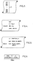
- FIG. 4 Another known method of the state of the art (see FIG. 4) proposes to implement a software loop including the NOP instruction above, and whose number of iterations is a function of the duration of the state waiting that we want to generate. This method is advantageous when N is great because it is less expensive in terms of memory space storing the program of the application.
- a disadvantage of this method lies in the implementation of the software loop that requires four instructions and, by therefore, four cycles of microprocessor instruction for processing an iteration of the loop (to be multiplied by the number of iterations of the loop).
- Another disadvantage of this method is that the implementation also requires a counting register.
- a last known method of the state of the art proposes waiting for an interruption or an external event, in which case the duration the waiting state is not determined because it depends on when produces said interruption or said external event.
- this method requires storing in an external memory the restart address of the program execution of the application.
- she is not precise as to when the state should be triggered waiting time and as regards the duration itself of this state of waiting.
- This solution is therefore suitable for generating very long waiting states in systems that do not require high accuracy.
- This method is not suitable however not for some computer or telecommunication systems whose applications are very sensitive to the execution time (applications real time for example).
- the present invention proposes generate a waiting state for a corresponding determined period of time typically to a determined number of clock cycles by executing a single instruction, so-called waiting instruction, while avoiding as much as possible the solicitation of the integrated circuits that make up the microprocessor during this waiting state.
- the invention thus relates to a microprocessor comprising a unit calculation that includes logical units to perform operations associated with specific instructions from a set of instructions of the microprocessor and a control unit to interpret the instructions and to control logical drives accordingly.
- the microprocessor further comprises an internal timer which is activated by the control unit in response to the execution of an instruction dedicated microprocessor instruction set, said waiting instruction, and which delivers a timing signal delivered to the control unit for place the microprocessor in a waiting state for a period of determined delay.
- an instruction dedicated microprocessor instruction set said waiting instruction
- the implementation of such an instruction reduces considerably the memory allocated for the program processed by the microprocessor.
- the control unit to place the microprocessor in the standby state, the control unit generates a blocking signal for interrupt and block the processing of instructions for the duration of delay.
- the units which normally perform operations associated with respective instructions are no longer requested during the duration of the timing and thus are in a low power sleep state energy.
- the timer may be programmable, the delay time being a function of a value specified as a parameter of the standby instruction.
- the duration of time delay can for example correspond to a fixed number of microprocessor clock cycles. The program to implement a state waiting for several clock cycles is thus greatly reduced since a only dedicated instruction of the microprocessor instruction set is necessary, and gains in flexibility of use in case of modification of the delay time.
- control unit comprises a recovery unit to retrieve instructions to execute that are stored in a program memory and a sequencer that receives the timing signal.
- sequencer can deliver the blocking signal on an activation input and disabling said recovery unit to interrupt and block the retrieval of instructions.
- the control unit may further comprise a decoding unit to decode instructions to execute. So, the sequencer can deliver the blocking signal on an input for activating and deactivating said unit decoding to interrupt and block the decoding of instructions.
- control unit also has a register instruction to store an instruction to execute.
- sequencer can also deliver the blocking signal on an activation input and disabling said instruction register to interrupt and block the storage of instructions to execute.
- the control unit may also include an ordinal counter which stores the address of a future instruction to execute.
- the sequencer can deliver the blocking signal on an activation input and disabling said counter to interrupt and block address storage in the meter.
- the microprocessor has an architecture pipeline and / or RISC architecture.
- a parameterization option allows to set the delay time, said duration being a value specified as a parameter of the standby instruction.
- control unit comprises a sequencer that receives the timing signal and processing units instructions including at least one recovery unit to recover in a program memory instructions to execute.
- sequencer delivers the blocking signal on a activation and deactivation input of said recovery unit so to interrupt and block the retrieval of instructions for the duration of delay.
- control unit may also include at least one decoding unit for decoding instructions to execute.
- sequencer can deliver the blocking signal on an activation and deactivation input of said recovery unit so to interrupt and block the retrieval of instructions for the duration of delay.
- the control unit may comprise at least one register instruction that stores instructions to execute.
- the sequencer can deliver the blocking signal to an input activating and deactivating said instruction register in order to interrupt and block the storage of instructions in said register for the duration of delay.
- the control unit may comprise at least one ordinal counter which stores the address of the next instruction to execute.
- the sequencer can deliver the blocking signal on a activation and deactivation input of said counter in order to interrupt and block address storage during the timeout period.
- Figure 1 illustrates an embodiment of a microprocessor 10 according to the invention.
- the microprocessor 10 comprises a computing unit 12 (or unit execution) to perform operations associated with instructions belonging to a set of instructions once decoded, and a unit of command 14 to interpret the instructions and to control the calculation unit accordingly, to the rhythm of clock cycles H.
- the microprocessor 10 includes an internal timer 34 and programmable preference. It may be for example a counter made at average JK flip-flops.
- the timer 34 is controlled by a signal of SC command generated by the sequencer 16 in response to the execution of a single instruction dedicated instruction set of the microprocessor 10, called waiting instruction.
- the delay time is a function of a parameter specified in parameter of the standby statement.
- the waiting instruction then comprises a first field containing the code of the statement and a second field containing the value of the duration of delay.
- the delay time can be set equal to one determined number N of clock cycles, with N strictly greater than unit.
- the timer Once the timer has been controlled, it emits a delay ST towards the sequencer 16 which emits a blocking signal SB to the recovery unit 22.
- the blocking signal SB is delivered on an input EN1 activation and deactivation, called “input ENABLE "of the recovery unit 22 so that said unit is deactivated to interrupt the retrieval of instructions from the memory of program 24.
- Sequencer 16 no longer delivers control signals to the computing unit 12, the microprocessor 10 is in a state of waiting for a determined period corresponding to a determined number of clock cycles. Generally, we speaks of "freezing" of the microprocessor to designate such a state of waiting.
- the computing unit 12 no longer being controlled during the state waiting, it is in a passive state (or standby state) in which it does not consumes very little power because the logical drives it contains do not perform basic operations.
- the blocking signal SB is delivered on an input EN2 activation and deactivation, called "ENABLE entry", of the decoding 26 which, accordingly, is deactivated and no longer decodes instructions.
- the blocking signal SB is delivered on a EN3 activation and deactivation input, called "ENABLE input", of the instruction register 20 which, accordingly, is deactivated and no longer stores the instructions to be executed.
- the blocking signal SB is delivered on a EN4 activation and deactivation input, called "ENABLE input", of the ordinal counter 18 which, consequently, is deactivated and no longer stores the addresses of the instructions to be executed.
- An application of the invention relates to microprocessors presenting a RISC architecture and therefore a pipeline architecture where code optimization is an essential factor for good performance.
- the generation of a waiting state of several cycles clock by executing a single wait instruction is particularly advantageous.
- an instruction is processed in a cycle of instructions which includes among other things a research cycle, a cycle of decoding, a run cycle and a write cycle, each of these four cycles being performed in a respective clock cycle. So, an instruction is processed, in a conventional microprocessor, according to four clock cycles.
- the pipeline architecture allows for simultaneous processing of multiple instructions. For example, she starts executing an instruction without wait for the end of the previous one.
- an instruction is applied in input of the computing unit, while a second is decoded and a third is retrieved from an external memory. Therefore, the duration of processing of an instruction can be of a clock cycle only.
- the timer 34 delivers a signal of ST delay to the sequencer 16 which then delivers a blocking signal SB to a unit of the pipeline architecture as a recovery unit 22 or a decoding unit 26.
- the processing of the instructions is thus interrupted and blocked as described previously.
- the microprocessor 10 is then in a state of waiting for a determined period corresponding to a determined number of clock cycles. There is also talk of "freezing" the microprocessor or "freezes" the pipeline.
- the invention also applies to 8-bit microprocessors, 16-bit, 32-bit or larger which respectively deal with 8-bit instructions, 16 bits, 32 bits or more, the bit size of the instruction does not influence the implementation of the method.
- Figure 2 illustrates, in flowchart form, the steps of a example of a method for managing a waiting state of a microprocessor according to the present invention.
- the method includes an optional parameterizing step 1 for set the duration of the waiting state to be generated, that is to say for example the number of clock cycles of the waiting state.
- This step is of course performed during the code development phase of the application that is intended to be executed in the microprocessor 10.
- the duration is a value specified as a parameter of the standby statement. For example, for a wait instruction referenced WAIT in the code and for a duration of 8 clock cycles, we write "WAIT 8" in the code listing.
- the waiting instruction is processed according to the instruction cycle already described above.
- step 3 the sequencer 16 controls the timer 34 which is thus activated and which delivers in a step 4 a delay signal ST which is delivered to the sequencer 16.
- the sequencer 16 interrupts and blocks temporarily processing the instructions in response to the signal from ST delay.
- the sequencer 16 delivers a blocking signal SB to the recovery unit 22 and / or the decoding unit 26 and / or the register instruction 20 and / or the ordinal counter 18, as has been said above.
- the microprocessor 10 is thus in a state of waiting for a period of time determined.
- timer 34 delivers the delay signal ST at sequencer 16
- said sequencer blocks the processing of the instructions.
- step 6 the sequencer 16 no longer delivers blocking signal SB and in parallel disables timer 34. The processing of instructions resumes normal and the microprocessor exits the waiting state.
Landscapes
- Engineering & Computer Science (AREA)
- Software Systems (AREA)
- Theoretical Computer Science (AREA)
- Physics & Mathematics (AREA)
- General Engineering & Computer Science (AREA)
- General Physics & Mathematics (AREA)
- Executing Machine-Instructions (AREA)
- Advance Control (AREA)
Applications Claiming Priority (2)
| Application Number | Priority Date | Filing Date | Title |
|---|---|---|---|
| FR0402816 | 2004-03-18 | ||
| FR0402816A FR2867873A1 (fr) | 2004-03-18 | 2004-03-18 | Dispositif et procede de gestion d'un etat d'attente d'un microprocesseur |
Publications (1)
| Publication Number | Publication Date |
|---|---|
| EP1596285A2 true EP1596285A2 (de) | 2005-11-16 |
Family
ID=34896628
Family Applications (1)
| Application Number | Title | Priority Date | Filing Date |
|---|---|---|---|
| EP05290595A Withdrawn EP1596285A2 (de) | 2004-03-18 | 2005-03-17 | Vorrichtung und Verfahren zur Verwaltung des Wartezustands in einem Mikroprocessor |
Country Status (3)
| Country | Link |
|---|---|
| US (1) | US7421595B2 (de) |
| EP (1) | EP1596285A2 (de) |
| FR (1) | FR2867873A1 (de) |
Cited By (1)
| Publication number | Priority date | Publication date | Assignee | Title |
|---|---|---|---|---|
| KR101137457B1 (ko) * | 2010-04-01 | 2012-04-20 | 주식회사 메타바이오메드 | 생분해성 말초신경도관 제조방법 및 그에 의한 말초신경도관 |
Families Citing this family (1)
| Publication number | Priority date | Publication date | Assignee | Title |
|---|---|---|---|---|
| CN111064556A (zh) * | 2019-11-22 | 2020-04-24 | 深圳市元征科技股份有限公司 | 一种通讯指令处理方法及设备 |
Family Cites Families (27)
| Publication number | Priority date | Publication date | Assignee | Title |
|---|---|---|---|---|
| US2279498A (en) * | 1937-10-22 | 1942-04-14 | Benjamin F Schmidt | Pump |
| US3577190A (en) | 1968-06-26 | 1971-05-04 | Ibm | Apparatus in a digital computer for allowing the skipping of predetermined instructions in a sequence of instructions, in response to the occurrence of certain conditions |
| US4484303A (en) | 1979-06-19 | 1984-11-20 | Gould Inc. | Programmable controller |
| US4482983A (en) * | 1980-06-23 | 1984-11-13 | Sperry Corporation | Variable speed cycle time for synchronous machines |
| JP2610821B2 (ja) | 1986-01-08 | 1997-05-14 | 株式会社日立製作所 | マルチプロセツサシステム |
| US5551033A (en) | 1991-05-17 | 1996-08-27 | Zenith Data Systems Corporation | Apparatus for maintaining one interrupt mask register in conformity with another in a manner invisible to an executing program |
| JP2748822B2 (ja) * | 1993-07-05 | 1998-05-13 | 日本電気株式会社 | 情報処理装置 |
| US5584031A (en) * | 1993-11-09 | 1996-12-10 | Motorola Inc. | System and method for executing a low power delay instruction |
| US6116768A (en) | 1993-11-30 | 2000-09-12 | Texas Instruments Incorporated | Three input arithmetic logic unit with barrel rotator |
| US5781750A (en) | 1994-01-11 | 1998-07-14 | Exponential Technology, Inc. | Dual-instruction-set architecture CPU with hidden software emulation mode |
| GB9419246D0 (en) | 1994-09-23 | 1994-11-09 | Cambridge Consultants | Data processing circuits and interfaces |
| US5974240A (en) | 1995-06-07 | 1999-10-26 | International Business Machines Corporation | Method and system for buffering condition code data in a data processing system having out-of-order and speculative instruction execution |
| CN1280714C (zh) | 1996-08-27 | 2006-10-18 | 松下电器产业株式会社 | 独立处理多个指令流、软式控制各指令流的处理功能的多线程处理器 |
| JPH10124315A (ja) | 1996-10-18 | 1998-05-15 | Hitachi Ltd | 分岐処理方法およびそのための情報処理装置 |
| US5805850A (en) | 1997-01-30 | 1998-09-08 | International Business Machines Corporation | Very long instruction word (VLIW) computer having efficient instruction code format |
| US6125449A (en) | 1997-06-30 | 2000-09-26 | Compaq Computer Corporation | Controlling power states of a computer |
| US5805491A (en) | 1997-07-11 | 1998-09-08 | International Business Machines Corporation | Fast 4-2 carry save adder using multiplexer logic |
| JP2000112585A (ja) | 1998-10-02 | 2000-04-21 | Toshiba Corp | システムlsi及びパワーマネジメント方法 |
| US6505313B1 (en) | 1999-12-17 | 2003-01-07 | Lsi Logic Corporation | Multi-condition BISR test mode for memories with redundancy |
| US20030070013A1 (en) * | 2000-10-27 | 2003-04-10 | Daniel Hansson | Method and apparatus for reducing power consumption in a digital processor |
| WO2002077799A1 (en) * | 2001-03-22 | 2002-10-03 | Infineon Technologies Ag | Program-controlled unit employing a stop instruction |
| US7142612B2 (en) | 2001-11-16 | 2006-11-28 | Rambus, Inc. | Method and apparatus for multi-level signaling |
| JP2005510792A (ja) * | 2001-11-26 | 2005-04-21 | コーニンクレッカ フィリップス エレクトロニクス エヌ ヴィ | 可変プロセッサ、および、このようなプロセッサのための命令集合、ディスパッチ方法、コンパイル方法 |
| US7191350B2 (en) | 2002-01-30 | 2007-03-13 | Matsushita Electric Industrial Co., Ltd. | Instruction conversion apparatus and instruction conversion method providing power control information, program and circuit for implementing the instruction conversion, and microprocessor for executing the converted instruction |
| JP3816845B2 (ja) | 2002-07-05 | 2006-08-30 | 富士通株式会社 | プロセッサ及び命令制御方法 |
| US6978361B2 (en) | 2002-09-20 | 2005-12-20 | International Business Machines Corporation | Effectively infinite branch prediction table mechanism |
| US7197655B2 (en) * | 2003-06-26 | 2007-03-27 | International Business Machines Corporation | Lowered PU power usage method and apparatus |
-
2004
- 2004-03-18 FR FR0402816A patent/FR2867873A1/fr active Pending
-
2005
- 2005-03-17 EP EP05290595A patent/EP1596285A2/de not_active Withdrawn
- 2005-03-17 US US11/083,111 patent/US7421595B2/en not_active Expired - Fee Related
Cited By (1)
| Publication number | Priority date | Publication date | Assignee | Title |
|---|---|---|---|---|
| KR101137457B1 (ko) * | 2010-04-01 | 2012-04-20 | 주식회사 메타바이오메드 | 생분해성 말초신경도관 제조방법 및 그에 의한 말초신경도관 |
Also Published As
| Publication number | Publication date |
|---|---|
| FR2867873A1 (fr) | 2005-09-23 |
| US20050216778A1 (en) | 2005-09-29 |
| US7421595B2 (en) | 2008-09-02 |
Similar Documents
| Publication | Publication Date | Title |
|---|---|---|
| US6304955B1 (en) | Method and apparatus for performing latency based hazard detection | |
| US6564313B1 (en) | System and method for efficient instruction prefetching based on loop periods | |
| EP1619589A1 (de) | Verfahren zur Programmierung einer System auf Chip DMA Steuerung, sowie ein System auf Chip dafür. | |
| FR2770659A1 (fr) | Processeur de traitement perfectionne | |
| JP2015144002A (ja) | 単一方向回転子のためのレジスタベースのシフト | |
| EP1983439B1 (de) | Prefetching basierend auf Streaming-Hinweisen | |
| EP0931287B1 (de) | Asynchrone datenverarbeitungsvorrichtung | |
| US8028180B2 (en) | Method and system for power conservation in a hierarchical branch predictor | |
| KR101077425B1 (ko) | 효율적 인터럽트 리턴 어드레스 저장 메커니즘 | |
| JP2001022593A (ja) | 割り込み可能なマルチサイクル命令を処理する方法および装置 | |
| US8135909B2 (en) | System for starting a preload of a second program while a first program is executing | |
| FR2678400A1 (fr) | Processeur de protocole destine a l'execution d'un ensemble d'instructions en un nombre reduit d'operation. | |
| FR2867873A1 (fr) | Dispositif et procede de gestion d'un etat d'attente d'un microprocesseur | |
| KR101759411B1 (ko) | 보안 보조 프로세서 부팅 성능 | |
| JP5371569B2 (ja) | データ処理装置及び制御方法及びプログラム | |
| EP1596286A2 (de) | Vorrichtung und Verfahren zur Verwaltung des Wartezustands in einem Mikroprozessor | |
| JPH06295243A (ja) | データ処理装置 | |
| CN100430889C (zh) | 在数字信号处理器系统中的存储器访问方法 | |
| WO2007098006A2 (en) | Execution of instructions directly from input source | |
| CN116635833A (zh) | 复杂cpu上的精确时间戳或导出计数器值生成 | |
| JP2001236220A (ja) | マイクロプロセッサの命令プリフェッチ量制御のための装置および方法 | |
| CN116627622A (zh) | 一种数据处理方法、装置、设备及存储介质 | |
| EP1596282A2 (de) | Vorrichtung und Verfahren zur Verwaltung des Befehlsatzes in einem Mikroprozessor | |
| US20040230915A1 (en) | System and method for improved distributed menu performance | |
| Brain | How microprocessors work |
Legal Events
| Date | Code | Title | Description |
|---|---|---|---|
| PUAI | Public reference made under article 153(3) epc to a published international application that has entered the european phase |
Free format text: ORIGINAL CODE: 0009012 |
|
| AK | Designated contracting states |
Kind code of ref document: A2 Designated state(s): AT BE BG CH CY CZ DE DK EE ES FI FR GB GR HU IE IS IT LI LT LU MC NL PL PT RO SE SI SK TR |
|
| AX | Request for extension of the european patent |
Extension state: AL BA HR LV MK YU |
|
| 17P | Request for examination filed |
Effective date: 20060127 |
|
| STAA | Information on the status of an ep patent application or granted ep patent |
Free format text: STATUS: THE APPLICATION IS DEEMED TO BE WITHDRAWN |
|
| 18D | Application deemed to be withdrawn |
Effective date: 20111001 |