Technical Field
The present invention relates to an optical module, wherein an
optical fiber and an optical semiconductor element are connected
optically.
Background Art
With the improvement and expansion of backbone
infrastructure in recent years, the focus of attention in the optical
communication market is being directed to the furnishing of user line
equipment and equipment for connecting user lines with the backbone.
Specifically, enhancement of metro area networks, access systems, and
school and company LANs and higher speeds and greater capacities in
provider's servers and routers are being desired.
In particular, optical connections in a school or company LAN
or among servers, routers, etc., within a provider are called VSR (Very
Short Reach) or interconnections. Although being short in distance,
signal transmissions of high speed and high volume are desired of such
optical connections. Since low cost is also desired, expensive
equipment, such as that required for optical connection at a transmission
rate of 10Gbps, is not suitable even if it enables high speed.
Due to such demands, optical modules for performing parallel
transmission of optical signals at a maximum rate of approximately
2.5Gbps are being noted. With such an optical module, a tape fiber,
which is an optical fiber array, and an optical semiconductor element
array are aligned and connected to transmit a plurality of optical signals
in parallel. However, if the alignment is performed by fiber alignment,
a low-cost optical module cannot be realized. Optical modules, with
which alignment is carried out by passive alignment, have thus been
proposed (Japanese Patent Application Laid-Open No. H7-77634,
Japanese Patent Application Laid-Open No. H7-151940).
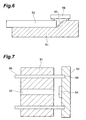
FIG. 7 is a sectional view showing an arrangement example of
a conventional passive alignment type optical module (see the document,
"IEICE Technical Report LQE99-130, pp.1-6"). The alignment of an
optical fiber 92 and an optical semiconductor element 94 is carried out
by the insertion and adhesion of guide pins 95, provided in a fiber
ferrule 91, into guide pin insertion holes 96 provided in a substrate 93.
Here, the optical fiber 92 is inserted in a fiber insertion portion that is
aligned with respect to the guide pins 95 and optical semiconductor
element 94 is aligned and fixed on the substrate 93 using an aligning
mark, formed by the same mask process as the guide pin insertion holes
96, as a guide:
Disclosure of the Invention
With all optical modules of the conventional passive alignment
type, the mounting of the optical fiber is performed at an early stage of
the assembly process of the entire optical module. For example, with
the optical module shown in FIG. 7, in the case where the substrate 93 is
to be mounted onto a circuit substrate as a sub-mount, the substrate 93 is
fixed upon being erected perpendicular to the circuit substrate for
suppressing the module height. In this case, it will be difficult to
mount the fiber ferrule 91 to the substrate 93 after the substrate 93 has
been fixed to the circuit substrate. The mounting of the fiber ferrule 91,
with the optical fiber 92, onto the substrate 93, with the optical
semiconductor element 94, is thus performed prior to the step of fixing
the substrate 93 to the circuit substrate.
When such a step of mounting the optical fiber is carried out at
an early stage of assembling the entire optical module, handling and
automation in subsequent steps may be hindered. For example, in a
step wherein the optical semiconductor element or the substrate
provided with the optical semiconductor element is to be die-bonded or
wire-bonded, etc., to the circuit substrate, a specialized device that takes
into consideration that the optical fiber has been mounted already will
be required. Such situations have hindered mass production and cost
reduction of optical modules.
The present invention has been made to resolve the above
issues, and an object thereof is to provide an optical module suitable for
mass production and cost reduction.
In order to achieve the above object, the present invention's
optical module comprises: (1) a sub-mount, having an optical
semiconductor element, disposed on a predetermined first surface, and a
first alignment portion, which is formed on the first surface; (2) a fiber
fixing member, having a fixing groove, which is formed on a
predetermined second surface and is for aligning and fixing an optical
fiber, a concave mirror, which is disposed with respect to the fixing
groove and guides light emitted from one of either the optical fiber that
is fixed to the fixing groove and the corresponding optical
semiconductor element to the other, and a second alignment portion,
which is formed on the second surface; and (3) the optical fiber, fixed to
the fixing groove; and wherein (4) of the first alignment portion and the
second alignment portion, one of either comprises a guide rail and the
other comprises a guide groove that fit with the guide rail, and the sub-mount
and the fiber fixing member are aligned and fixed by fitting
together of the first alignment portion and the second alignment portion.
With the above-described optical module, the optical
semiconductor element and the optical fiber are aligned by the fitting
together of the first alignment portion of the sub-mount and the second
alignment portion of the fiber fixing member. Alignment by passive
alignment is thus enabled with this optical module.
Also, since the guide rail and the guide groove are used as the
alignment portions, the optical semiconductor element and the optical
fiber can be aligned at high precision.
Also, the second surface of the fiber fixing member, onto
which the optical fiber is fixed, is positioned to face the first surface of
the sub-mount, on which the optical semiconductor element is disposed.
The step of aligning and fixing the fiber fixing member, to which the
optical fiber is fixed, with respect to the sub-mount can thereby be
performed after a step of die-bonding or wire-bonding, etc., the sub-mount
to a circuit substrate. An optical module can thus be realized
with which the handling and automation in the step of die-bonding or
wire-bonding, etc., the sub-mount to the circuit substrate will not be
hindered and with which mass production and cost reduction are
enabled. Also, since the optical fiber is positioned parallel to the first
surface of the sub-mount, the module height is kept low.
Furthermore, a concave mirror is disposed as a light guiding
optical system between the optical fiber and the optical semiconductor
element. Since the light that is emitted from one of either of the
optical fiber and the optical semiconductor element is thereby
converged and guided to the other, a high optical coupling factor can be
realized.
The optical module may have an arrangement wherein the sub-mount
has N (N being an integer no less than 2) of the optical
semiconductor elements, the fiber fixing member has N of the fixing
grooves that are mutually parallel and N of the concave mirrors,
disposed, respectively, with respect to the N fixing grooves, and N of
the optical fibers are, respectively, fixed in the N fixing grooves. In
this case, since a plurality of optical signals can be transmitted in
parallel, an optical module enabling transmission of higher speed and
greater volume is provided.
Also, the optical semiconductor element may be prepared from
the same material and by the same semiconductor process as the sub-mount
and thereby formed to be monolithic with the first alignment
portion. Or, the sub-mount may have an aligning mark formed by the
same mask process as the first alignment portion and the optical
semiconductor element may be disposed by being aligned with respect
to the sub-mount using the aligning mark as a reference. In these cases,
a sub-mount, with which the optical semiconductor element and the first
alignment portion are aligned at high precision with respect to each
other, can be obtained.
Also, the fiber fixing member may be molded integrally from
resin. In this case, a fiber fixing member, with which the fixing groove,
the concave mirror, and the second alignment portion are aligned at high
precision with respect to each other, can be obtained.
Also, the second alignment portion may be formed
substantially parallel to the fixing groove. In this case, the second
alignment portion and the fixing groove can be formed readily while
being aligned with respect to each other.
Also, the cross-sectional shape of the guide rail in the plane
perpendicular to the longitudinal direction thereof may be a tapered
shape. In this case, the fitting together of the guide rail and the guide
groove is facilitated.
Also, the optical module may be equipped with a lens, which is
disposed between the optical semiconductor element and the concave
mirror and converge the light emitted from one of either the optical fiber
and the corresponding optical semiconductor element to the other. In
this case, the optical coupling factor can be improved further in
accompaniment with the convergence by the concave mirror.
Also, as the optical semiconductor element to be disposed on
the sub-mount, a photodetecting element may be used. In this case, the
optical module becomes an optical receiving module. Or, a light
emitting element may be used as the optical semiconductor element.
In this case, the optical module becomes an optical transmitting module.
Brief Description of the Drawings
FIG. 1 is a sectional side view showing the arrangement of an
embodiment of an optical module.
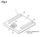
FIG. 2 is a perspective view of a sub-mount equipped in the
optical module shown in FIG. 1.
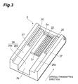
FIG. 3 is a perspective view of a fiber fixing member equipped
in the optical module of FIG. 1.
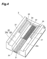
FIG. 4 is a perspective view showing the state wherein optical
fibers are fixed to the fiber fixing member shown in FIG. 3.
FIG. 5 is a sectional front view taken on line I-I of the optical
module shown in FIG. 1.
FIG. 6 is a sectional side view showing an arrangement
example of a passive alignment type optical module.
FIG. 7 is a sectional view showing an arrangement example of
a conventional passive alignment type optical module.
Best Modes for Carrying Out the Invention
Preferred embodiments of the present invention's optical
module shall now be described along with the drawings. In the
description of the drawings, the same elements shall be provided with
the same symbols and redundant description shall be omitted. The
dimensional proportions of the drawings do not necessarily match those
of the descriptions.
FIG. 1 is a sectional side view showing the arrangement of an
embodiment of the present invention's optical module. The
arrangement of this embodiment's optical module shall be described in
outline using FIG. 1. This optical module is an optical module for
optical transmission or optical receiving that transmits or receives
optical signals in parallel and has N (where N is a natural number)
optical fibers optically connected with N optical semiconductor
elements. With the embodiment to be described below, N = 4. Also,
FIG. 1 shows the cross-sectional view in the plane containing the optical
axes of one set among four sets of the optical fiber and the optical
semiconductor element. In FIG. 1, the left-to-right direction is the
direction of optical transmission along the optical axis of the optical
fiber.
The present optical module is equipped with a circuit substrate
41, a sub-mount 1, a fiber fixing member 2, and a coated optical fiber
array 31. The circuit substrate 41 is a mounting substrate on which
sub-mount 1 is mounted. Wirings, electronic circuits, etc., necessary
for signal processing are also mounted on the circuit substrate 41. In
FIG. 1, a pre-amplifier 43, which amplifies and outputs an electrical
signal, is mounted on the circuit substrate 41.
The sub-mount 1 is a substrate for installing the optical
semiconductor element. This sub-mount 1 is set on the circuit
substrate 41. The surface of the sub-mount 1 at the side opposite the
side of the circuit substrate 41 is an optical element mounting surface
(first surface) 16 on which the optical semiconductor element is
disposed. For example, a silicon substrate may be used as the substrate
of the sub-mount 1.
A photodiode array 11 is disposed on the optical element
mounting surface 16. This photodiode array 11 is an optical
semiconductor element array, with which four photodiodes
(photodetecting elements) 12 are arrayed at a fixed pitch as the optical
semiconductor elements. These photodiodes 12 are disposed with a
direction perpendicular to the optical axes of the optical fibers 3 to be
described later (the direction perpendicular to the paper surface in FIG.
1) as the array direction. The pre-amp 43 on the circuit substrate 41,
the photodiode array 11 on the sub-mount 1, and the electrodes, wirings,
etc., disposed on the circuit substrate 41 and sub-mount 1 are
electrically connected by die-bonding or wire-bonding, etc.
The fiber fixing member 2 is a member that fixes the optical
fibers. With respect to the sub-mount 1, this fiber fixing member 2 is
installed at the side opposite the side of the circuit substrate 41. The
surface of the fiber fixing member 2 that faces the optical element
mounting surface 16 of the sub-mount 1 is an optical fiber fixing surface
(second surface) 26 to which the optical fibers are fixed. The fiber
fixing member 2 may, for example, be molded integrally from resin.
On the optical fiber fixing surface 26, four V-grooves 21 are
formed in parallel as fixing grooves for aligning and fixing the optical
fibers. The coated optical fiber array 31, having four optical fibers
arrayed at a fixed pitch, is installed with respect to the V-grooves 21.
The coating is removed across a predetermined length at a front end
portion of the coated optical fiber array 31, thereby exposing four
optical fibers 3. These exposed optical fibers 3 are aligned and fixed,
respectively, in the corresponding V-grooves 21.
These V-grooves 21 and optical fibers 3 that are fixed to the V-grooves
21 are arrayed in a direction perpendicular to the optical axes of
the optical fibers 3 and are positioned at the same pitch as the
photodiodes 12 so as to correspond thereto. Also, along with an
optical fiber fixing portion 2a, which is positioned above the sub-mount
1 and is provided with the V-grooves 21, the fiber fixing member 2 is
provided with an array housing portion 2b, which protrudes in the
direction in which the coated optical fiber array 31 extends from the
sub-mount 1 and the optical fiber fixing portion 2a.
Also, on the optical fiber fixing surface 26, concave mirrors 22
are disposed at positions on the optical axes and opposing the end faces,
respectively, of the optical fibers 3. These concave mirrors 22 are
provided, respectively, for the four V-grooves 21 and optical fibers 3.
The concave mirrors 22 are also positioned on the upwardly directed
optical axes of the corresponding photodiodes 12 as viewed from the
sub-mount 1. Each concave mirror 22 converts the optical path of the
light emitted from the end face of an optical fiber 3 vertically downward
by substantially 90°, converts the light to parallel light, and guides the
light while converging it toward a photodiode 12.
Between the concave mirrors 22 and photodiodes 12, ball
lenses 14 are aligned so that their optical axes are matched to the optical
axes of the photodiodes 12. Each ball lens 14 converges the light,
emitted from the optical fiber 3 and converted in the optical path by the
concave mirror 22, onto the corresponding photodiode 12. With the
present embodiment, a light guiding optical system between the optical
fibers 3 and photodiodes 12 is arranged by the concave mirrors 22 and
ball lenses 14. The ball lenses 14 can be aligned, for example, by
fixing onto lens mounting pedestals formed using resist, etc., in the
same semiconductor process as the photodiode array 11.
The above-mentioned circuit substrate 41, sub-mount 1, fiber
fixing member 2, etc., are housed in a casing 45, comprising a casing
body portion 44a, and a casing cover portion 44b positioned above the
casing body portion 44a. On a bottom portion 45a of the casing body
portion 44a, the circuit substrate 41 is disposed with the surface, at the
side opposite the surface on which the sub-mount 1 is mounted, facing
the bottom portion 45a.
An opening 47 is provided on the optical axes of the optical
fibers 3 at a side portion 45b, which, among the side portions of the
casing 45, is at the array housing portion 2b side as viewed from the
optical fiber fixing portion 2a. The coated optical fiber array 31 is
passed through this opening 47.
The opening 47, through which the coated optical fiber array
31 is passed, is filled with a solder 48. This solder 48 fixes the coated
optical fiber array 31 to the casing 45 and closes the opening 47 and
thereby keeps the casing 45 airtight. When the coated optical fiber
array 31 is fixed by the solder 48 in this manner, the use of a metal
coating, such as that of a metallized fiber, is preferable as the coating of
the coated optical fiber array 31. Or, the coated optical fiber array 31
may be fixed to the casing 45 by a resin, etc.
At a side portion 45c of the casing 45 that opposes the side
portion 45b is inserted output terminals 42. These output terminals 42
guide, to the exterior of the casing, the electrical signals from the
photodiodes 12 that have been amplified by the pre-amps 43.
FIG. 2 is a perspective view of the sub-mount 1 as viewed from
the side of the fiber fixing member 2. The arrangement of the sub-mount
1 shall now be described in detail using FIG. 2.
On the optical element mounting surface 16 of the sub-mount
1, two guide grooves 10, which extend in parallel to each other, are
formed as first alignment portions. The guide grooves 10 are for
aligning the optical fibers 3 and photodiodes 12 by passive alignment.
The direction in which these guide grooves 10 are formed is
perpendicular to the array direction of the photodiodes 12. Also, the
guide grooves 10 are disposed at predetermined positions corresponding
to second alignment portions equipped on the fiber fixing member 2.
The cross-sectional shape in the plane perpendicular to the longitudinal
direction of each guide groove 10 is a tapered shape that becomes
gradually narrow in width from the optical element mounting surface 16
toward the inner side of the sub-mount 1.
Also, on the optical element mounting surface 16 is formed an
aligning mark 13. This aligning mark 13 serves as a reference in
aligning and fixing the photodiode array 11 with respect to the sub-mount
1. The aligning mark 13 is aligned with respect to the two
guide grooves 10 and is preferably formed by the same mask process as
the guide grooves 10.
With respect to aligning mark 13, the photodiode array 11 is
installed at a position at the upstream side in the optical transmitting
direction of the optical fibers 3. The photodiode array 11 can be fixed
to the sub-mount 1, for example, by flip-chip bonding. The Guide
grooves 10, which are the first alignment portions, are aligned with
respect to the photodiode array 11.
FIG. 3 is a perspective view of the fiber fixing member 2 as
viewed form the sub-mount 1 side. The arrangement of the fiber
fixing member 2 shall now be described in detail using FIG 3.
On the optical fiber fixing surface 26 of the fiber fixing
member 2, two guide rails 20, which extend in parallel to each other, are
formed as second alignment portions. The guide rails 20 are fitted
with the guide grooves 10 to align the optical fibers 3 and photodiodes
12 by passive alignment. As with the guide grooves 10, the cross-sectional
shape in the plane perpendicular to the longitudinal direction
of each guide rail 20 is a tapered shape that becomes gradually narrow
in width from the optical fiber fixing surface 26 toward the sub-mount 1
side. The direction in which the guide rails 20 are formed is parallel to
the direction in which the V-grooves 21 are formed.
The optical fiber fixing surface 26 is formed so that as viewed
in the array direction of the optical fibers 3, which is a direction
perpendicular to the optical transmitting direction, the central portion is
depressed along the optical transmitting direction. This depressed
portion is a V-groove forming portion 26a at which the V-grooves 21 for
fixing the optical fibers 3 are formed. By this arrangement, the
distances between the optical fibers 3 and concave mirrors 22, which are
installed on the optical fiber fixing surface 26, and the photodiodes 12,
which are installed on the optical element mounting surface 16 of the
sub-mount 1, are set favorably.
With the present embodiment, the upstream side portion in the
optical transmitting direction of the V-groove forming portion 26a is the
array housing portion 2b, and the downstream side portion is the optical
fiber fixing portion 2a. As described using FIG. 1, four V-grooves 21,
extending along the optical transmitting direction, are formed in the
optical fiber fixing portion 2a, and four concave mirrors 22 are disposed
further at the downstream side.
As viewed in the direction in which the optical fibers 3 are
arrayed, the respective sides of the V-groove forming portion 26a are
guide rail forming portions 26b. The two above-mentioned guide rails
20 are disposed, respectively, at the guide rail forming portions 26b at
the respective sides so as to sandwich the four V-grooves 21 formed at
the V-groove forming portion 26a. The guide rails 20, which are the
second alignment portions, are aligned with respect to the V-grooves 21,
and the optical fibers 3 fixed to the V-grooves 21. With the inclusion
of the V-groove forming portion 26a and guide rail forming portions
26b, the width of the optical fiber fixing surface 26 in the array direction
of the optical fibers 3 is substantially matched to the width of the sub-mount
1.
At the respective sides of the optical fiber fixing surface 26 at
the outer sides of guide rail forming portions 26b as viewed in the array
direction of the optical fibers 3 are provided with the guide portions 27.
These guide portions 27 protrude toward the side at which the sub-mount
1 is positioned as viewed from the optical fiber fixing surface 26
and are the portions that guide the fitting of the guide rails 20 with the
guide grooves 10 in the process of aligning and fixing the fiber fixing
member 2 with respect to the sub-mount 1. The height of protrusion of
these guide portions 27 is set smaller than the height of the sub-mount 1.
FIG. 4 is a perspective view showing the state wherein the
coated optical fiber array 31 and optical fibers 3 are fixed to the fiber
fixing member 2 shown in FIG. 3. As shown in FIG. 4, the optical
fibers 3 are fixed, respectively, to the four V-grooves 21. This fixing is
carried out by placing the optical fibers 3 in the V-grooves 21 and
adhesively fixing by an adhesive agent. In the process of fixing, a
glass plate, etc., may be used as a fiber holder.
FIG. 5 is a sectional front view taken on line I-I of the optical
module shown in FIG. 1. The fiber fixing member 2 is set so that its
guide portions 27 sandwich the sub-mount 1 from both sides and guide
rail forming portions 26b of the optical fiber fixing surface 26 of the
fiber fixing member 2 contacts the optical element mounting surface 16
of the sub-mount 1. At that point, as shown in FIG. 5, the guide
grooves 10, formed in the sub-mount 1 and guide rails 20, formed on
the fiber fixing member 2, fit together. The photodiodes 12, which are
aligned with respect to the guide grooves 10, and optical fibers 3, which
are aligned with respect to the guide rails 20, are thereby aligned by
passive alignment.
The fiber fixing member 2 and circuit substrate 41, below the
sub-mount 1, are fixed by an adhesive agent. In FIG. 5, an adhesive
agent 46, which is filled between the lower surface of the guide portions
27 of the fiber fixing member 2 and the upper surface of the circuit
substrate 41, is shown.
A process of assembling the present optical module shall now
be described using FIG. 1. The circuit substrate 41 is mounted to the
casing body portion 44a. The sub-mount 1 and pre-amps 43 are
furthermore mounted to the circuit substrate 41. The mounting can be
performed by die-bonding by a resin or wire-bonding by gold wires or
aluminum wires, etc.
Meanwhile, as a separate process from the process of
mounting the sub-mount 1, the optical fibers 3 are fixed to the fiber
fixing member 2. By then fitting the guide rails 20 in the guide
grooves 10, the fiber fixing member 2, to which the optical fibers 3 are
fixed, is aligned and fixed with respect to the sub-mount 1. In this
state, adhesive agent 46 is filled in the predetermined spaces to
adhesively fix the fiber fixing member 2 to the circuit substrate 41.
Lastly, by passing the coated optical fiber array 31 through the
opening 47 and sealingly fixing the casing cover portion 44b on the
casing body portion 44a, the optical module is completed. This fixing
in a sealing manner can be performed by adhesive fixing using a resin.
The effects of the optical module of the present embodiment
shall now be described. With the present optical module, the optical
fibers 3 and photodiodes 12 are aligned by the fitting together of the
guide grooves 10 of the sub-mount 1 and guide rails 20 of the fiber
fixing member 2. Alignment by passive alignment is thus realized
with the present optical module.
Also, the guide grooves 10 are used as first alignment portions
and guide rails 20 are used as second alignment portions. The optical
fibers 3 and photodiodes 12 are thus aligned at high precision. Guide
rails may be used instead as the first alignment portions formed on the
sub-mount 1, and guide grooves may be used as the second alignment
portions formed on the fiber fixing member 2.
Also, since the optical fiber fixing surface 26 is disposed so as
to oppose the optical element mounting surface 16, the step of aligning
and fixing the fiber fixing member 2, to which the optical fibers 3 are
fixed, with respect to the sub-mount 1 can be performed after the step of
die-bonding or wire-bonding, etc., the sub-mount 1 to the circuit
substrate 41. Handling and automation of the step of die-bonding or
wire-bonding, etc., the sub-mount 1 to the circuit substrate 41 will thus
not be hindered. The present optical module thus enables mass
production and cost reduction. Also, with the present optical module,
since the optical fibers 3 are disposed parallel to the optical element
mounting surface 16 of the sub-mount 1, the module height is kept low.
Furthermore, the concave mirrors 22 are provided as the light
guiding optical system between the optical fibers 3 and photodiodes 12.
Since light emitted from the optical fibers 3 are thereby converged and
guided to the photodiodes 12, a high optical coupling factor is realized.
Also, with the present embodiment, the concave mirrors 22
make the light from the optical fibers 3 parallel light. Since the light
from optical fibers 3 thus propagate as parallel light along the optical
paths from the concave mirrors 22 to the ball lenses 14, the tolerance of
the optical module is relaxed. For example, calculations using an
optical simulator have shown that optical coupling is enabled even when
the positional relationship between the concave mirrors 22 and
photodiodes 12 is moved by approximately ±40µm. The concave
mirrors 22 are not necessarily limited to those that convert the reflected
light into parallel light.
Also, with the present optical module, since pluralities of the
optical fibers 3 and photodiodes 12 are provided, respectively, a
plurality of optical signals can be transmitted in parallel. An optical
module, enabling high-speed, high-volume transmission, is thus realized.
Also, the ball lenses 14 for converging light are disposed
between the photodiodes 12 and concave mirrors 22. A high optical
coupling factor is thus realized. However, in the case where an
adequate optical coupling factor is obtained by just the convergence by
the concave mirrors 22, the ball lenses 14 do not have to be provided.
Such cases include the case where single mode fibers with a core
diameter of 10µm are used as the optical fibers 3 and the case where the
photodiodes 12 that are used have an adequately large photodetecting
diameter.
The ball lenses 14 can be aligned by fixing onto lens mounting
pedestals formed using a resist, etc., in the same semiconductor process
as that of the photodiode array 11. The ball lenses 14 can thereby be
aligned at a precision of within ±1 to 2µm in this case.
Also, in the case where the aligning mark 13 and guide
grooves 10 are formed by the same mask process, the aligning mark 13
can be aligned at a precision of within ±1 to 2µm with respect to the
guide grooves 10. Thus, in this case, the photodiode array 11 and
guide grooves 10 can be aligned at high precision with respect to each
other.
The photodiode array 11 can be prepared from the same
material and by the same semiconductor process as the sub-mount 1 and
thereby formed to be monolithic to the guide grooves 10. The
photodiode array 11 and guide grooves 10 are aligned at high precision
with respect to each other when formed in this manner as well. In this
case, the aligning mark 13 need not be formed as it is unnecessary.
In the case where the photodiode array 11 is mounted to the
sub-mount 1 by flip-chip bonding, alignment can be performed at a
precision of within ±5 µm.
Also, in the case where the fiber fixing member 2 is integrally
molded from resin, it can be prepared at a high precision wherein the
precision of the respective pitches of the V-grooves 21 and concave
mirrors 22, the relative positional relationship of the V-grooves 21 and
concave mirrors 22, and relative positional relationship of the guide
rails 20 and V-grooves 21 are within ±10µm. The fiber fixing member
2 may also be molded integrally using an MIM (Metal Injection Mold).
With this type of molding, the precision can be made as high as in the
case of integral molding from resin.
Also, in the fiber fixing member 2, an adhesive agent having a
refractive index matching characteristic can be filled between the
optical fibers 3 and concave mirrors 22. The returning light from the
front ends of the optical fibers 3 can thereby be restrained.
Also, the guide rails 20 are formed substantially parallel to the
V-grooves 21. The guide rails 20 and V-grooves 21 can thus be
aligned and formed readily. Furthermore, since the guide rails 20 are
formed, respectively, on the guide rail forming portions 26b at the
respective sides of the V-grooves 21, sub-mount 1 and the fiber fixing
member 2 are aligned at high precision.
Also, the cross-sectional shapes in the plane perpendicular to
the longitudinal direction of the guide grooves 10 and guide rails 20 are
tapered shapes. The guide grooves 10 and guide rails 20 can thus be
fitted together readily. Also, since the fiber fixing member 2 is
provided with the guide portions 27, the fitting of the guide grooves 10
and guide rails 20 can be performed readily in a single step.
Optical modules, with which optical fibers and optical
semiconductor elements are aligned by the fitting of guide rails and
guide grooves, are also described in Japanese Patent Application Laid-Open
No. H7-77634 and Japanese Patent Application Laid-Open No.
H7-151940.
In Japanese Patent Application Laid-Open No. H7-77634 is
described an optical module, wherein optical fibers and optical
semiconductor elements are aligned by passive alignment by the fitting
of guide rails, formed on a substrate to which the optical fibers are fixed,
with guide grooves that are directly formed in the optical semiconductor
elements.
However, this optical module has an arrangement wherein the
optical fibers and the optical semiconductor elements are positioned
along the same optical axis. Thus, portions for mounting the optical
semiconductor elements must be provided on the substrate and along the
optical axis in addition to the fixing portions for the optical fibers.
This optical module thus cannot be made compact.
Meanwhile, the present invention's optical module has an
arrangement wherein, the concave mirrors 22, which convert the optical
paths of the light emitted from the optical fibers 3, are provided and the
light from the optical fibers 3 are made incident on the photodiodes 12
at positions opposing the optical fiber fixing surface 26. There is thus
no need to provide portions for mounting the photodiodes 12 on the
fiber fixing member 2. The present optical module can thus be made
compact.
Also, in Japanese Patent Application Laid-Open No. H7-151940
is described an optical module, wherein an alignment substrate
is provided in addition to a fiber fixing member and a sub-mount.
However, with this optical module, an alignment portion must
be formed not just on the fiber fixing member 2 and sub-mount but on
the substrate as well. The step of forming the alignment portions and
thus the process of manufacturing the entire optical module becomes
complicated. Also, since there are two independent locations where
alignment portions fit with each other (that is, the two locations for the
fitting of the fiber fixing member with the substrate and the fitting of the
sub-mount with the substrate), alignment errors will be amplified.
Meanwhile, with the present invention's optical module,
alignment portions 10 and 20 are provided just at the sub-mount 1 and
fiber fixing member 2 and these are fitted directly to perform alignment.
Thus, with this optical module, the manufacturing process is simplified
and alignment is carried out at high precision.
Also, as a passive alignment type optical module, the
arrangement shown in FIG. 6 may be considered for example. With
the optical module of FIG. 6, the alignment of an optical fiber 82 and an
optical semiconductor element 84 is carried out by means of a V-groove
and an aligning mark that have been formed on a substrate 81 by the
same mask process. A planar mirror 85, which guides light between
the optical fiber 82 and optical semiconductor element 84 is provided on
the substrate 81.
However, with this optical module, since the optical fiber 82
enters below the optical semiconductor element 84, the optical
semiconductor element 84 is flip-chip mounted using the alignment
mark as a guide after adhesively fixing the optical fiber 82 in the V-groove.
Handling and automation in the step of flip-chip mounting the
optical semiconductor element 84 are thus hindered. This optical
module thus does not enable mass production and cost reduction.
Meanwhile, with the optical module of FIG. 1, the fiber fixing
member 2, to which the optical fibers 3 have been fixed, can be aligned
and fixed with respect to the sub-mount 1 after die-bonding or wire-bonding,
etc., the sub-mount 1 to the circuit substrate 41. This optical
module can thus be mass-produced and reduced in cost.
Also, with the optical module of FIG. 6, the rear surface (the
surface at the side opposite the photodetecting surface) of the optical
semiconductor element 84 is floated. Heat thus cannot be dissipated
efficiently from the optical semiconductor element 84. This becomes a
cause of unstable operation of the optical module, especially in the case
of a VCSEL (Vertical Cavity Surface Emitting Laser) or other element
of high heat generation amount.
Meanwhile, with the optical module of FIG. 1, since the
photodiodes 12 are disposed on the sub-mount 1, the rear surfaces
thereof are not floated. Heat can thus be dissipated efficiently from the
photodiodes 12.
Also, with an optical module, such as that shown in FIG. 6 or 7,
the optical coupling factor is low since a concave mirror or other
converging optical system is not used. That is, when high-speed
operation of approximately 2.5Gbps is considered, an element with a
photodetecting diameter of 40 to 80µm is normally used as the optical
semiconductor element 84 or 94. Meanwhile, the distance along the
optical axis from the optical fiber 82 or 92 to the optical semiconductor
element 84 or 94 must be set to no less than the fiber cladding diameter
(125µm) in the case of the arrangement of FIG. 6 and no less than the
loop height (approximately 100µm) of the wires used in bonding in the
case of the arrangement of FIG. 7. Consequently, the spot diameter on
the optical semiconductor element 84 or 94 will be 117.5µm in the case
of a core diameter of 62.5µm and a numerical aperture of 0.275 and will
be 92µm in the case of a core diameter of 50µm, and thus the total light
amount cannot be detected by the optical semiconductor element 84 or
94. The optical coupling factor will be lowered especially in the case
where a multimode fiber of large core diameter and numerical aperture
is used.
On the other hand, with the optical module of FIG. 1, since the
light from the optical fibers 3 are converged and guided by the concave
mirrors 22 to the photodiodes 12, a high optical coupling factor is
realized.
An example of the optical design of the present invention's
optical module shall now be described. Here, it shall be assumed that
as each of the optical fibers 3, a multimode fiber with a core diameter of
62.5µm and a numerical aperture of 0.275 is used, and as each of the
photodiodes 12, a photodiode, having a photodetecting diameter of
80µm and enabled to perform high-speed operation of up to 2.5Gbps, is
used. Also, the array pitch of the photodiodes 12 in the photodiode
array 11 is 250µm.
In this case, in order to prevent cross-talk, in which the light
from one optical fiber 3 becomes incident on the photodetecting
portions of two or more the photodiodes 12, the spreading of the light
flux must be restrained to be no more than 200pm in consideration of a
margin. The upper limit of the interval between the optical fibers 3
and concave mirrors 22 is thus 250µm.
Meanwhile, the interval between the concave mirrors 22 and
photodiodes 12 must be set to no less than 250µm in consideration of
space for bonding wires, even if the ball lenses 14 are not to be provided.
In addition, since the distance from the reflection centers of the concave
mirrors 22 to the optical fibers 3 must also be considered, the interval
between the concave mirrors 22 and photodiodes 12 must be set to no
less than 312.5µm. In the case where a glass plate, etc., is provided as
an optical fiber holder, since the thickness thereof must be considered,
the lower limit of the above-mentioned interval will be greater than
312.5µm.
By the above, in the present invention's optical module, the
interval between the concave mirrors 22 and photodiodes 12 will be
greater than the interval between the optical fibers 3 and concave
mirrors 22 and the optical system will be a magnifying system. Even
with an arrangement wherein the latter interval is set to the upper limit
of 250µm and the former interval is set to the lower limit of 312.5µm,
the magnification will be 1.25 and the image of a core of 62.5µm
diameter will be an image of 78µm diameter on a photodiode 12.
Although the photodetecting diameter of each photodiode 12 is 80µm,
in consideration of the tolerances of the manufacture and assembly of
the respective members 1 and 2, it will be difficult to realize an optical
coupling factor of 100%.
Thus, with the present optical module, by providing a
converging optical system of the concave mirrors 22, etc., the light from
the optical fibers 3 are guided to the photodiodes 12 upon being
converged. An optical coupling factor of 100% can thus be realized
with this optical module.
Although in the optical module shown in FIG. 1 to FIG. 5, N,
which expresses the number of the optical fibers 3, the number of the
photodiodes 12, etc., is set to 4, this number N may be set as suited.
When is N is set to 2 or more, since a plurality of optical signals can be
transmitted in parallel as described above, transmission at higher speed
and greater volume is enabled. Even when N is set to 1, the same
effects as the optical module shown in FIG. 1 to FIG. 5 are exhibited in
regard to the alignment of the optical fiber 3 and photodiode 12, etc.
Also, as the optical semiconductor element, a photodetecting
element besides photodiode 12 may be used, or a light emitting element,
such as a VCSEL, may be used. In the case where a light emitting
element is used, the concave mirror 22 guides the light emitted from the
light emitting element to the optical fiber 3 and the ball lens 14
converges the light emitted from the light emitting element.
Industrial Applicability
The present invention's optical module can be used as an
optical module suitable for mass production and cost reduction. That
is, with the present invention's optical module, the optical fiber and the
optical semiconductor element are aligned by the fitting together of the
first alignment portion and the second alignment portion. Alignment
of the optical fiber and optical semiconductor element by passive
alignment is thus realized.
Also, since the guide rail and the guide groove are used as the
alignment portions, the optical fiber and the optical semiconductor
element are aligned at high precision.
Also, the step of aligning and fixing the fiber fixing member,
to which the optical fiber is fixed, with respect to the sub-mount can be
performed after the step of die-bonding or wire-bonding, etc., the sub-mount
to the circuit substrate. An optical module that enables mass
production and cost reduction is thus realized. Also, since the optical
fiber is disposed in parallel to the first surface of the sub-mount, the
module height is kept low.
Furthermore, the concave mirror is disposed as the light
guiding optical system between the optical fiber and the optical
semiconductor element. Since the light emitted from one of either of
the optical fiber and the optical semiconductor element is thereby
converged and guided to the other, a high optical coupling factor is
realized.