EP1594168A1 - Solar cell panel - Google Patents
Solar cell panel Download PDFInfo
- Publication number
- EP1594168A1 EP1594168A1 EP04708487A EP04708487A EP1594168A1 EP 1594168 A1 EP1594168 A1 EP 1594168A1 EP 04708487 A EP04708487 A EP 04708487A EP 04708487 A EP04708487 A EP 04708487A EP 1594168 A1 EP1594168 A1 EP 1594168A1
- Authority
- EP
- European Patent Office
- Prior art keywords
- solar cell
- series
- cell assembly
- solar
- assembly series
- Prior art date
- Legal status (The legal status is an assumption and is not a legal conclusion. Google has not performed a legal analysis and makes no representation as to the accuracy of the status listed.)
- Granted
Links
Images


Classifications
-
- H—ELECTRICITY
- H10—SEMICONDUCTOR DEVICES; ELECTRIC SOLID-STATE DEVICES NOT OTHERWISE PROVIDED FOR
- H10F—INORGANIC SEMICONDUCTOR DEVICES SENSITIVE TO INFRARED RADIATION, LIGHT, ELECTROMAGNETIC RADIATION OF SHORTER WAVELENGTH OR CORPUSCULAR RADIATION
- H10F19/00—Integrated devices, or assemblies of multiple devices, comprising at least one photovoltaic cell covered by group H10F10/00, e.g. photovoltaic modules
- H10F19/90—Structures for connecting between photovoltaic cells, e.g. interconnections or insulating spacers
- H10F19/902—Structures for connecting between photovoltaic cells, e.g. interconnections or insulating spacers for series or parallel connection of photovoltaic cells
- H10F19/904—Structures for connecting between photovoltaic cells, e.g. interconnections or insulating spacers for series or parallel connection of photovoltaic cells characterised by the shapes of the structures
-
- H—ELECTRICITY
- H10—SEMICONDUCTOR DEVICES; ELECTRIC SOLID-STATE DEVICES NOT OTHERWISE PROVIDED FOR
- H10F—INORGANIC SEMICONDUCTOR DEVICES SENSITIVE TO INFRARED RADIATION, LIGHT, ELECTROMAGNETIC RADIATION OF SHORTER WAVELENGTH OR CORPUSCULAR RADIATION
- H10F19/00—Integrated devices, or assemblies of multiple devices, comprising at least one photovoltaic cell covered by group H10F10/00, e.g. photovoltaic modules
- H10F19/90—Structures for connecting between photovoltaic cells, e.g. interconnections or insulating spacers
- H10F19/902—Structures for connecting between photovoltaic cells, e.g. interconnections or insulating spacers for series or parallel connection of photovoltaic cells
-
- H—ELECTRICITY
- H10—SEMICONDUCTOR DEVICES; ELECTRIC SOLID-STATE DEVICES NOT OTHERWISE PROVIDED FOR
- H10F—INORGANIC SEMICONDUCTOR DEVICES SENSITIVE TO INFRARED RADIATION, LIGHT, ELECTROMAGNETIC RADIATION OF SHORTER WAVELENGTH OR CORPUSCULAR RADIATION
- H10F77/00—Constructional details of devices covered by this subclass
- H10F77/30—Coatings
- H10F77/306—Coatings for devices having potential barriers
- H10F77/311—Coatings for devices having potential barriers for photovoltaic cells
-
- Y—GENERAL TAGGING OF NEW TECHNOLOGICAL DEVELOPMENTS; GENERAL TAGGING OF CROSS-SECTIONAL TECHNOLOGIES SPANNING OVER SEVERAL SECTIONS OF THE IPC; TECHNICAL SUBJECTS COVERED BY FORMER USPC CROSS-REFERENCE ART COLLECTIONS [XRACs] AND DIGESTS
- Y02—TECHNOLOGIES OR APPLICATIONS FOR MITIGATION OR ADAPTATION AGAINST CLIMATE CHANGE
- Y02E—REDUCTION OF GREENHOUSE GAS [GHG] EMISSIONS, RELATED TO ENERGY GENERATION, TRANSMISSION OR DISTRIBUTION
- Y02E10/00—Energy generation through renewable energy sources
- Y02E10/50—Photovoltaic [PV] energy
Definitions
- the present invention relates to a solar cell panel for use in spacecrafts, such as satellites and airships. More particularly, it relates to a solar cell array and a solar cell panel structure that can prevent electrical discharges from occurring between any solar cells.
- a prior art solar cell panel in which an insulating material, such as an RTV adhesive, is filled into the gap between solar cells in the solar cell panel and is used as an insulating barrier is known as a measure for preventing an electric discharge from occurring between the solar cells (refer to patent reference 1, for example).
- Patent reference 1 Japanese patent application publication No. 11-274,542 (see Figs. 11 and 18)
- the prior art solar cell panel in which an insulating material, such as an RTV adhesive, is placed in the gap between solar cells in the solar cell panel and is used as an insulating barrier has the following problems.
- the first problem is that the prior art solar cell panel increases in weight by only the weight of the adhesive which is used as the insulating barrier.
- the second problem is that the prior art solar cell panel increases in cost because of increase in the material cost of the adhesive which is used as the insulating barrier, the cost of installing the insulating barrier, increase in the cost of launching a rocket, and so on.
- any two adjacent solar cell assembly series are so connected as to have different gradient directions in their potentials with respect to a folded connection point therebetween, any two adjacent solar cells in any two adjacent solar cell assembly series have a minimum potential difference of 0 volts at their lowermost ends and a maximum potential difference of 2V volts at their uppermost ends when each solar cell assembly series has a potential difference of V volts.
- the uppermost ends of any two adjacent solar cell assembly series having the maximum potential difference are at increased risk of causing electrostatic discharges.
- an adequate margin of safety can be provided against electric discharges if the voltages of solar cells are reduced to 1/2 or less of original ones, as compared with a case where an insulating barrier is provided between any solar cells (refer to paragraph number (0049) of patent reference 1). Therefore, implementation of an arrangement of solar cells which can reduce the potential difference between any two adjacent solar cells is effective in preventing electric discharges from occurring between any solar cells.
- the present invention is made in order to solve the above-mentioned problems, and it is therefore an object of the present invention to provide a solar cell panel that can prevent electric discharges from occurring between any solar cells without installing an insulating barrier in the gap between any solar cells.
- a solar cell panel including: a plurality of solar cell assembly series each including a plurality of solar cells and interconnectors each for electrically connecting between two of these solar cells in series, said plurality of solar cells being arranged substantially in a line and any two of said plurality of solar cells being electrically connected in series by one of said interconnectors; an insulator on which said plurality of solar cell assembly series are arranged at predetermined gaps; and connection lines that electrically connect said plurality of adjacent solar cell assembly series so that they are connected in series, said plurality of solar cell assembly series being arranged so that they have an identical gradient direction in their potentials.
- a solar cell panel including: a plurality of solar cell assembly series each including a plurality of solar cells and interconnectors each for electrically connecting between two of these solar cells in series, said plurality of solar cells being arranged substantially in a line and any two of said plurality of solar cells being electrically connected in series by one of said interconnectors; an insulator on which said plurality of solar cell assembly series are arranged at predetermined gaps; first connection lines that electrically connect some of said plurality of solar cell assembly series so that they are connected in series so as to form a first solar cell string; and second connection lines that electrically connect remaining ones of said plurality of solar cell assembly series so that they are connected in series so as to form a second solar cell string, the solar cell assembly series of said first solar cell string and the solar cell assembly series of said second solar cell string being arranged so that they are surely adjacent to one another.
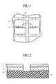
- Fig. 1 is a plan view showing embodiment 1 of the present invention.
- solar cells 2 are secured to a surface of an insulator 1.
- Interconnectors 3 are connected to each of the solar cells 2, and a cover glass 4 is bonded to each of the solar cells 2.
- Fig. 2 is a cross-sectional view showing a cross section of Fig. 1 taken along the line 5-5.
- each solar cell 2 is secured to the surface of the insulator 1 by an adhesive 6, and the cover glass 4 is secured to the light receiving surface of each solar cell 2 by an adhesive 7.
- Fig. 3 is a diagram showing the structure of solar cell circuitry according to embodiment 1 of the present invention.
- n solar cell assemblies 8 each having a maximum output voltage u are arranged substantially in a line so that each solar cell assembly series 9 is constructed.
- N solar cell assembly series 9 are electrically connected in series by way of connection lines 10 so that a solar cell string 11 is constructed.
- the last solar cell assembly of the first solar cell assembly series 9a which is located at the lowermost end thereof shown in the figure is electrically connected in series with the first solar cell assembly of the second solar cell assembly series 9b which is located at the uppermost end thereof shown in the figure by a connection line 10.
- any two adjacent solar cells in the first and second solar cell assembly series can have a potential difference which does not exceed V.
- any two adjacent solar cells have a maximum potential difference of 2V volts.
- the potential difference between any two adjacent solar cells in any two adjacent solar cell assembly series is greatly reduced to V volts which is the maximum output voltage of each solar cell assembly series or less.
- Fig. 1 is a plan view showing embodiment 2 of the present invention.
- Fig. 2 is a cross-sectional view showing a cross section of Fig. 1 taken along the line 5-5.
- Fig. 4 is a diagram showing solar cell circuitry according to embodiment 2 of the present invention.
- n solar cell assemblies 8a each having a maximum output voltage u are arranged substantially in a line so that each solar cell assembly series 9a is constructed.
- N solar cell assembly series 9a are electrically connected in series by way of connection lines 10 so that a solar cell string 11a is constructed.
- n solar cell assemblies 8b each having a maximum output voltage u are arranged substantially in a line so that each solar cell assembly series 9b is constructed.
- N solar cell assembly series 9b are electrically connected in series by way of connection lines 10 so that a solar cell string 11b is constructed.
- the solar cell string 11a and the solar cell string 11b are connected in parallel so that a solar cell module 12 is constructed.
- the first series of the N solar cell assembly series 9a is arranged at the leftmost end of the solar cell module, and the first series of the N solar cell assembly series 9b is arranged at the rightmost end of the solar cell module.
- the first series of the N solar cell assembly series 9a is so arranged as to have a direction of potential difference between 0 volts at its uppermost end and V volts at its lowermost end
- the first series of the N solar cell assembly series 9b is so arranged as to have a direction of potential difference between 0 volts at its lowermost end and V volts at its uppermost end.
- the first series of the N solar cell assembly series 9a and the second series of the N solar cell assembly series 9b are so arranged as to be adjacent to each other. Therefore, since the solar cells in the first solar cell assembly series 9a which are running from the uppermost end thereof shown in the figure have respective potentials u, 2u, ..., (n-1)*u, and n*u, and the solar cells in the second solar cell assembly series 9b which are running from the uppermost end thereof shown in the figure have respective potentials V+u, V+2u, ... , V+(n-1)*u, and V+n*u, any two adjacent solar cells in the first solar cell assembly series 9a and the second solar cell assembly series 9b can have a potential difference which does not exceed V.
- any other solar cell assembly series 9a which constitutes the solar cell string 11a in the solar cell module and a corresponding solar cell assembly series 9b which constitutes the other solar cell string 11b connected in parallel with the solar cell string 11a are so arranged as to be adjacent to each other.
- any two adjacent solar cells have a maximum potential difference of 2V volts.
- the potential difference between any two adjacent solar cells in any two adjacent solar cell assembly series is greatly reduced to V volts which is the maximum output voltage of each solar cell assembly series or less.
- Fig. 1 is a plan view showing embodiment 3 of the present invention.
- Fig. 2 is a cross-sectional view showing a cross section of Fig. 1 taken along the line 5-5.
- Fig. 5 is a diagram showing solar cell circuitry according to embodiment 3 of the present invention.
- n solar cell assemblies 8a each having a maximum output voltage u are arranged substantially in a line so that each solar cell assembly series 9a is constructed.
- N solar cell assembly series 9a are electrically connected in series by way of connection lines 10 so that a solar cell string 11a is constructed.
- n solar cell assemblies 8b each having a maximum output voltage u are arranged substantially in a line so that each solar cell assembly series 9b is constructed.
- N solar cell assembly series 9b are electrically connected in series by way of connection lines 10 so that a solar cell string 11b is constructed.
- the solar cell string 11a and the solar cell string 11b are connected in parallel so that a solar cell module 12a is constructed.
- n solar cell assemblies 8c each having a maximum output voltage u are arranged substantially in a line so that each solar cell assembly series 9c is constructed.
- N solar cell assembly series 9c are electrically connected in series by way of connection lines 10 so that a solar cell string 11c is constructed.
- n solar cell assemblies 8d each having a maximum output voltage u are arranged substantially in a line so that each solar cell assembly series 9d is constructed.
- N solar cell assembly series 9d are electrically connected in series by way of connection lines 10 so that a solar cell string 11d is constructed.
- the solar cell string 11c and the solar cell string 11d are connected in parallel so that a solar cell module 12b is constructed.
- the first series of the N solar cell assembly series 9a and the second series of the N solar cell assembly series 9b are so arranged as to be adjacent to each other. Therefore, since the solar cells in the first series of the N solar cell assembly series 9a which are running from the uppermost end thereof shown in the figure have respective output potentials u, 2u, ..., (n-1)*u, and n*u, and the solar cells in the second series of the N solar cell assembly series 9b which are running from the uppermost end thereof shown in the figure have respective output potentials V+u, V+2u, ..., V+(n-1)*u, and V+n*u, any two adjacent solar cells in the first series of the N solar cell assembly series 9a and the second series of the N solar cell assembly series 9b can have a potential difference which does not exceed V.
- any other solar cell assembly series 9a which constitutes the solar cell string 11a in the solar cell module 12a and a corresponding solar cell assembly series 9b which constitutes the other solar cell string 11b connected in parallel with the solar cell string 11a are so arranged as to be adjacent to each other. Therefore, any two adjacent solar cells in any two adjacent solar cell assembly series 9a and 9b in the solar cell module 12a can have a potential difference which does not exceed V.
- the first series of the N solar cell assembly series 9c and the second series of the N solar cell assembly series 9d are so arranged as to be adjacent to each other. Therefore, since the solar cells in the first series of the N solar cell assembly series 9c which are running from the uppermost end thereof shown in the figure have respective output potentials u, 2u, ..., (n-1)*u, and n*u, and the solar cells in the second series of the N solar cell assembly series 9d which are running from the uppermost end thereof shown in the figure have respective output potentials V+u, V+2u, ..., V+(n-1)*u, and V+n*u, any two adjacent solar cells in the first series of the N solar cell assembly series 9c and the second series of the N solar cell assembly series 9d can have a potential difference which does not exceed V.
- any other solar cell assembly series 9c which constitutes the solar cell string 11c in the solar cell module 12b and a corresponding solar cell assembly series 9d which constitutes the other solar cell string 11d connected in parallel with the solar cell string 11c are so arranged as to be adjacent to each other. Therefore, any two adjacent solar cells in any two adjacent solar cell assembly series 9c and 9d in the solar cell module 12b can have a potential difference which does not exceed V.
- the solar cell module 12a and the solar cell module 12b are so arranged that they are point symmetric to each other with respect to a center of a boundary line between the solar cell module 12a and the solar cell module 12b, Therefore, since the first series of the N solar cell assembly series 9b and the first series of the N solar cell assembly series 9c are so arranged they are point symmetric to each other with respect to the center of the boundary line, the solar cells in the first series of the N solar cell assembly series 9b which are running from the uppermost end thereof shown in the figure have respective output potentials n*u, (n-1)*u,..., 2*u, and u, and the solar cells in the first series of the N solar cell assembly series 9c which are running from the uppermost end thereof shown in the figure have respective output potentials u, 2u, ... , (n-1)*u, and n*u. Therefore, the maximum potential of the solar cell assembly series within each solar cell module, which is arranged adjacent to the other solar cell module, can be reduced to the maximum output voltage V
- the potential difference between any two adjacent solar cells in any two solar cell assembly series of the solar cell panel, as well as the potential difference between the two adjacent solar cell modules, can be always reduced to the maximum output voltage V of each solar cell assembly series or less.
- electric discharges can be prevented from occurring between any solar cells in the solar cell panel.
- the weight of the solar cell panel can be reduced, the efficiency of mounting solar cells in the solar cell panel can be increased, and the cost of the solar cell panel can be reduced.
- an insulating barrier into the gap between any two solar cells, an adequate margin of safety can be provided against electric discharges between solar cells as compared with prior art solar cell panels.
- Fig. 1 is a plan view showing embodiment 4 of the present invention.
- Fig. 2 is a cross-sectional view showing a cross section of Fig. 1 taken along the line 5-5.
- Fig. 6 is a diagram showing solar cell circuitry according to embodiment 4 of the present invention.
- n solar cell assemblies 8a each having a maximum output voltage u are arranged substantially in a line so that each solar cell assembly series 9a is constructed.
- N solar cell assembly series 9a are electrically connected in series by way of connection lines 10 so that a solar cell string 11a is constructed.
- n solar cell assemblies 8b each having a maximum output voltage u are arranged substantially in a line so that each solar cell assembly series 9b is constructed.
- N solar cell assembly series 9b are electrically connected in series by way of connection lines 10 so that a solar cell string 11b is constructed.
- the solar cell string 11a and the solar cell string 11b are connected in parallel so that a solar cell module 12a is constructed.
- n solar cell assemblies 8c each having a maximum output voltage u are arranged substantially in a line so that each solar cell assembly series 9c is constructed.
- N solar cell assembly series 9c are electrically connected in series by way of connection lines 10 so that a solar cell string 11c is constructed.
- n solar cell assemblies 8d each having a maximum output voltage u are arranged substantially in a line so that each solar cell assembly series 9d is constructed.
- N solar cell assembly series 9d are electrically connected in series by way of connection lines 10 so that a solar cell string 11d is constructed.
- the solar cell string 11c and the solar cell string 11d are connected in parallel so that a solar cell module 12b is constructed.
- the first series of the N solar cell assembly series 9a and the second series of the N solar cell assembly series 9b are so arranged as to be adjacent to each other. Therefore, since the solar cells in the first series of the N solar cell assembly series 9a which are running from the uppermost end thereof shown in the figure have respective output potentials u, 2u, ..., (n-1)*u, and n*u, and the solar cells in the second series of the N solar cell assembly series 9b which are running from the uppermost end thereof shown in the figure have respective output potentials V+u, V+2u, ..., V+(n-1)*u, and V+n*u, any two adjacent solar cells in the first series of the N solar cell assembly series 9a and the second series of the N solar cell assembly series 9b can have a potential difference which does not exceed V.
- any other solar cell assembly series 9a which constitutes the solar cell string 11a in the solar cell module 12a and a corresponding solar cell assembly series 9b which constitutes the other solar cell string 11b connected in parallel with the solar cell string 11a are so arranged as to be adjacent to each other. Therefore, any two adjacent solar cells in any two adjacent solar cell assembly series 9a and 9b in the solar cell module 12a can have a potential difference which does not exceed V.
- the first series of the N solar cell assembly series 9c and the second series of the N solar cell assembly series 9d are so arranged as to be adjacent to each other. Therefore, since the solar cells in the first series of the N solar cell assembly series 9c which are running from the uppermost end thereof shown in the figure have respective output potentials u, 2u, ..., (n-1)*u, and n*u, and the solar cells in the second series of the N solar cell assembly series 9d which are running from the uppermost end thereof shown in the figure have respective output potentials V+u, V+2u, ..., V+(n-1)*u, and V+n*u, any two adjacent solar cells in the first series of the N solar cell assembly series 9c and the second series of the N solar cell assembly series 9d can have a potential difference which does not exceed V.
- any other solar cell assembly series 9c which constitutes the solar cell string 11c in the solar cell module 12b and a corresponding solar cell assembly series 9d which constitutes the other solar cell string 11d connected in parallel with the solar cell string 11c are so arranged as to be adjacent to each other. Therefore, any two adjacent solar cells in any two adjacent solar cell assembly series 9c and 9d in the solar cell module 12b can have a potential difference which does not exceed V.
- the solar cell module 12a and the solar cell module 12b are so arranged that they are line symmetric to each other with respect to a boundary line between the solar cell module 12a and the solar cell module 12b, Therefore, since the first series of the N solar cell assembly series 9b and the first series of the N solar cell assembly series 9c are so arranged they are line symmetric to each other with respect to the boundary line, the solar cells in the first series of the N solar cell assembly series 9b which are running from the uppermost end thereof shown in the figure have respective output potentials n*u, (n-1)*u,..., 2*u, and u, and the solar cells in the first series of the N solar cell assembly series 9c which are running from the uppermost end thereof shown in the figure have respective output potentials n*u, (n-1)*u,..., 2*u, and u.
- the solar cell assembly series within one solar cell module is therefore arranged at a potential difference of 0 volts with its neighboring solar cell assembly series within the other solar cell module.
- the solar cell assembly series pattern of the solar cell module 12a has line symmetry with respect to the solar cell assembly series pattern of the solar cell module 12b, the magnetic field caused by one of the two solar cell modules can be canceled by the magnetic field caused by the other solar cell module.
- the solar cell panel according to the present invention is suitable for use in spacecrafts, such as satellites and airships.
Landscapes
- Photovoltaic Devices (AREA)
- Life Sciences & Earth Sciences (AREA)
- Engineering & Computer Science (AREA)
- Sustainable Development (AREA)
- Sustainable Energy (AREA)
Abstract
Description
Claims (6)
- A solar cell panel characterized in that said solar cell panel comprises:a plurality of solar cell assembly series each including a plurality of solar cells and interconnectors each for electrically connecting between two of these solar cells in series, said plurality of solar cells being arranged substantially in a line and any two of said plurality of solar cells being electrically connected in series by one of said interconnectors;an insulator on which said plurality of solar cell assembly series are arranged at predetermined gaps; andconnection lines that electrically connect said plurality of adjacent solar cell assembly series so that they are connected in series, said plurality of solar cell assembly series being arranged so that they have an identical gradient direction in their potentials.
- A solar cell panel characterized in that said solar cell panel comprises:a plurality of solar cell assembly series each including a plurality of solar cells and interconnectors each for electrically connecting between two of these solar cells in series, said plurality of solar cells being arranged substantially in a line and any two of said plurality of solar cells being electrically connected in series by one of said interconnectors;an insulator on which said plurality of solar cell assembly series are arranged at predetermined gaps;first connection lines that electrically connect some of said plurality of solar cell assembly series so that they are connected in series so as to form a first solar cell string; andsecond connection lines that electrically connect remaining ones of said plurality of solar cell assembly series so that they are connected in series so as to form a second solar cell string;the solar cell assembly series of said first solar cell string and the solar cell assembly series of said second solar cell string being arranged so that they are surely adjacent to one another.
- The solar cell panel according to Claim 1, characterized in that said plurality of solar cell assembly series are arranged so as to be point symmetric with respect to a center of a boundary line between solar cell modules which are adjacent to each other, and solar cells located at the boundary between the solar cell modules have a maximum potential which is equal to or less than a maximum output voltage of said plurality of solar cell assembly series.
- The solar cell panel according to Claim 2, characterized in that said plurality of solar cell assembly series are arranged so as to be point symmetric with respect to a center of a boundary line between solar cell modules which are adjacent to each other, and solar cells located at the boundary between the solar cell modules have a maximum potential which is equal to or less than a maximum output voltage of said plurality of solar cell assembly series.
- The solar cell panel according to Claim 3, characterized in that said plurality of solar cell assembly series are arranged so as to be line symmetric with respect to a boundary line between solar cell modules which are adjacent to each other, and solar cells located at the boundary between the solar cell modules have a maximum potential which is equal to or less than a maximum output voltage of said plurality of solar cell assembly series.
- The solar cell panel according to Claim 4, characterized in that said plurality of solar cell assembly series are arranged so as to be line symmetric with respect to a boundary line between solar cell modules which are adjacent to each other, and solar cells located at the boundary between the solar cell modules have a maximum potential which is equal to or less than a maximum output voltage of said plurality of solar cell assembly series.
Applications Claiming Priority (3)
| Application Number | Priority Date | Filing Date | Title |
|---|---|---|---|
| JP2003033735A JP4003655B2 (en) | 2003-02-12 | 2003-02-12 | Solar panel |
| JP2003033735 | 2003-02-12 | ||
| PCT/JP2004/001200 WO2004073074A1 (en) | 2003-02-12 | 2004-02-05 | Solar cell panel |
Publications (3)
| Publication Number | Publication Date |
|---|---|
| EP1594168A1 true EP1594168A1 (en) | 2005-11-09 |
| EP1594168A4 EP1594168A4 (en) | 2006-04-19 |
| EP1594168B1 EP1594168B1 (en) | 2016-07-13 |
Family
ID=32866242
Family Applications (1)
| Application Number | Title | Priority Date | Filing Date |
|---|---|---|---|
| EP04708487.6A Expired - Lifetime EP1594168B1 (en) | 2003-02-12 | 2004-02-05 | Solar cell panel |
Country Status (4)
| Country | Link |
|---|---|
| US (2) | US9722119B2 (en) |
| EP (1) | EP1594168B1 (en) |
| JP (1) | JP4003655B2 (en) |
| WO (1) | WO2004073074A1 (en) |
Cited By (2)
| Publication number | Priority date | Publication date | Assignee | Title |
|---|---|---|---|---|
| CN101917135A (en) * | 2009-01-28 | 2010-12-15 | 英特赛尔美国股份有限公司 | Connection system and method for solar cells |
| CN104201981A (en) * | 2014-09-25 | 2014-12-10 | 阳光电源股份有限公司 | Anti-Potential Induced Degradation (PID) control method and control system |
Families Citing this family (8)
| Publication number | Priority date | Publication date | Assignee | Title |
|---|---|---|---|---|
| US8525369B2 (en) | 2010-06-02 | 2013-09-03 | GM Global Technology Operations LLC | Method and device for optimizing the use of solar electrical power |
| TW201244141A (en) * | 2011-04-29 | 2012-11-01 | Auria Solar Co Ltd | Thin film solar cell and fabricating method thereof |
| CN102956650A (en) * | 2011-08-26 | 2013-03-06 | 刘莹 | Novel laminated thin-film solar battery |
| JP5557820B2 (en) * | 2011-10-11 | 2014-07-23 | 株式会社コンテック | Solar power generation equipment |
| CN103050557B (en) * | 2011-10-12 | 2016-03-02 | 中建材浚鑫科技股份有限公司 | A kind of encapsulated circuit of solar cell string and solar module |
| US11575058B2 (en) * | 2017-06-30 | 2023-02-07 | Mitsubishi Electric Corporation | Solar power generator, solar array wing, and space structure |
| US10580919B2 (en) | 2017-12-07 | 2020-03-03 | Solaero Technologies Corp. | Space solar cell arrays with blocking diodes |
| CN113093813B (en) * | 2021-04-02 | 2023-09-29 | 阳光电源股份有限公司 | Reverse tracking method, controller and photovoltaic tracking system based on photovoltaic modules |
Family Cites Families (15)
| Publication number | Priority date | Publication date | Assignee | Title |
|---|---|---|---|---|
| US4019924A (en) * | 1975-11-14 | 1977-04-26 | Mobil Tyco Solar Energy Corporation | Solar cell mounting and interconnecting assembly |
| US4131123A (en) * | 1977-01-13 | 1978-12-26 | Solec International, Inc. | Solar cell module and method of making same |
| US4084985A (en) * | 1977-04-25 | 1978-04-18 | The United States Of America As Represented By The Administrator Of The National Aeronautics And Space Administration | Method for producing solar energy panels by automation |
| US4409537A (en) * | 1982-03-31 | 1983-10-11 | Honeywell Inc. | Interconnection of primary cells |
| DE3307202A1 (en) * | 1983-03-01 | 1984-09-06 | Siemens AG, 1000 Berlin und 8000 München | SOLAR CELL MODULE |
| JPH088372B2 (en) * | 1993-03-17 | 1996-01-29 | 日本電気株式会社 | Solar power supply |
| US5688337A (en) * | 1995-11-30 | 1997-11-18 | Texas Instruments Incorporated | Temperature compensated photovoltaic array |
| JPH10319851A (en) | 1997-05-14 | 1998-12-04 | Daido Hoxan Inc | Display panel by color solar batteries |
| US6248950B1 (en) * | 1998-02-21 | 2001-06-19 | Space Systems/Loral, Inc. | Solar array augmented electrostatic discharge for spacecraft in geosynchronous earth orbit |
| JP2000091617A (en) | 1998-09-08 | 2000-03-31 | Misawa Homes Co Ltd | Setting structure for solar battery panel |
| KR20000019144A (en) | 1998-09-09 | 2000-04-06 | 이수근 | Portable multi-power device using solar battery |
| JP2000312019A (en) * | 1999-02-25 | 2000-11-07 | Canon Inc | Photovoltaic module array, photovoltaic module array installation structure, photovoltaic module installation method, and photovoltaic power generation system |
| JP2001267617A (en) * | 2000-03-17 | 2001-09-28 | Daiwa House Ind Co Ltd | Installation structure of solar panels and solar cells |
| US6350944B1 (en) * | 2000-05-30 | 2002-02-26 | Hughes Electronics Corporation | Solar module array with reconfigurable tile |
| FR2822436B1 (en) * | 2001-03-21 | 2003-08-15 | Cit Alcatel | SOLAR PANEL HAVING ELECTRICAL TERMINALS DISTRIBUTED ON ITS SURFACE |
-
2003
- 2003-02-12 JP JP2003033735A patent/JP4003655B2/en not_active Expired - Lifetime
-
2004
- 2004-02-05 US US10/508,539 patent/US9722119B2/en active Active
- 2004-02-05 WO PCT/JP2004/001200 patent/WO2004073074A1/en not_active Ceased
- 2004-02-05 EP EP04708487.6A patent/EP1594168B1/en not_active Expired - Lifetime
-
2017
- 2017-04-20 US US15/492,824 patent/US20170222081A1/en not_active Abandoned
Cited By (2)
| Publication number | Priority date | Publication date | Assignee | Title |
|---|---|---|---|---|
| CN101917135A (en) * | 2009-01-28 | 2010-12-15 | 英特赛尔美国股份有限公司 | Connection system and method for solar cells |
| CN104201981A (en) * | 2014-09-25 | 2014-12-10 | 阳光电源股份有限公司 | Anti-Potential Induced Degradation (PID) control method and control system |
Also Published As
| Publication number | Publication date |
|---|---|
| EP1594168A4 (en) | 2006-04-19 |
| EP1594168B1 (en) | 2016-07-13 |
| JP4003655B2 (en) | 2007-11-07 |
| US9722119B2 (en) | 2017-08-01 |
| JP2004265926A (en) | 2004-09-24 |
| US20170222081A1 (en) | 2017-08-03 |
| WO2004073074A1 (en) | 2004-08-26 |
| US20050166954A1 (en) | 2005-08-04 |
Similar Documents
| Publication | Publication Date | Title |
|---|---|---|
| US20170222081A1 (en) | Solar cell panel | |
| US5919316A (en) | Spacecraft solar array design to control differential charging | |
| US6713670B2 (en) | Electrostatically clean solar array | |
| US20240235468A1 (en) | Single sheet foldout solar array | |
| US6903260B2 (en) | Solar panel having electrical terminals distributed across the surface thereof | |
| US20210013353A1 (en) | Single cell photovoltaic module | |
| US10014817B2 (en) | Flexible solar generator provided with electrical protection against the impact of celestial objects, spacecraft and satellite comprising at least one such solar generator | |
| US11817514B2 (en) | Blocking diode board for rollable solar power module | |
| US20190028057A1 (en) | Solar module and method for fabricating the same | |
| GB2224391A (en) | Anti-electrostatic panel | |
| US20120024337A1 (en) | Apparatus facilitating wiring of multiple solar panels | |
| US12490523B2 (en) | Solar cell array with changeable string length | |
| US20230021466A1 (en) | Photovoltaic module and flexible satellite solar generator | |
| CN113243051B (en) | Circuit arrangement for generating electricity using series-connected solar cells with bypass diodes | |
| JP6790265B2 (en) | Manufacturing method of photovoltaic power generation equipment, solar cell paddle, space structure and solar power generation equipment | |
| CN117397164A (en) | Solar cell module | |
| DE3935826A1 (en) | Solar plate structure for spacecraft - has conductive bead between elements to conductive coat on glass reducing undesired electrostatic fields | |
| CN111584660A (en) | Photovoltaic module and photovoltaic device including the same | |
| US12610627B2 (en) | Solar cell module | |
| JPS62229985A (en) | Solar battery panel device | |
| US11894175B2 (en) | System to optimize voltage distribution along high voltage doubler string | |
| EP4301095B1 (en) | Led module with surge current protection | |
| EP4589843A1 (en) | Output line connection structure for solar cell module |
Legal Events
| Date | Code | Title | Description |
|---|---|---|---|
| PUAI | Public reference made under article 153(3) epc to a published international application that has entered the european phase |
Free format text: ORIGINAL CODE: 0009012 |
|
| 17P | Request for examination filed |
Effective date: 20041012 |
|
| AK | Designated contracting states |
Kind code of ref document: A1 Designated state(s): AT BE BG CH CY CZ DE DK EE ES FI FR GB GR HU IE IT LI LU MC NL PT RO SE SI SK TR |
|
| AX | Request for extension of the european patent |
Extension state: AL LT LV MK |
|
| A4 | Supplementary search report drawn up and despatched |
Effective date: 20060306 |
|
| RAP1 | Party data changed (applicant data changed or rights of an application transferred) |
Owner name: MITSUBISHI DENKI KABUSHIKI KAISHA |
|
| DAX | Request for extension of the european patent (deleted) | ||
| RBV | Designated contracting states (corrected) |
Designated state(s): DE FR GB IT |
|
| 17Q | First examination report despatched |
Effective date: 20090622 |
|
| GRAP | Despatch of communication of intention to grant a patent |
Free format text: ORIGINAL CODE: EPIDOSNIGR1 |
|
| INTG | Intention to grant announced |
Effective date: 20160217 |
|
| GRAS | Grant fee paid |
Free format text: ORIGINAL CODE: EPIDOSNIGR3 |
|
| GRAA | (expected) grant |
Free format text: ORIGINAL CODE: 0009210 |
|
| AK | Designated contracting states |
Kind code of ref document: B1 Designated state(s): DE FR GB IT |
|
| REG | Reference to a national code |
Ref country code: GB Ref legal event code: FG4D |
|
| REG | Reference to a national code |
Ref country code: DE Ref legal event code: R096 Ref document number: 602004049577 Country of ref document: DE |
|
| REG | Reference to a national code |
Ref country code: FR Ref legal event code: PLFP Year of fee payment: 14 |
|
| REG | Reference to a national code |
Ref country code: DE Ref legal event code: R097 Ref document number: 602004049577 Country of ref document: DE |
|
| PLBE | No opposition filed within time limit |
Free format text: ORIGINAL CODE: 0009261 |
|
| STAA | Information on the status of an ep patent application or granted ep patent |
Free format text: STATUS: NO OPPOSITION FILED WITHIN TIME LIMIT |
|
| 26N | No opposition filed |
Effective date: 20170418 |
|
| REG | Reference to a national code |
Ref country code: FR Ref legal event code: PLFP Year of fee payment: 15 |
|
| REG | Reference to a national code |
Ref country code: DE Ref legal event code: R084 Ref document number: 602004049577 Country of ref document: DE |
|
| REG | Reference to a national code |
Ref country code: GB Ref legal event code: 746 Effective date: 20190117 |
|
| PGFP | Annual fee paid to national office [announced via postgrant information from national office to epo] |
Ref country code: IT Payment date: 20190221 Year of fee payment: 16 Ref country code: GB Payment date: 20190130 Year of fee payment: 16 |
|
| GBPC | Gb: european patent ceased through non-payment of renewal fee |
Effective date: 20200205 |
|
| PG25 | Lapsed in a contracting state [announced via postgrant information from national office to epo] |
Ref country code: GB Free format text: LAPSE BECAUSE OF NON-PAYMENT OF DUE FEES Effective date: 20200205 |
|
| PG25 | Lapsed in a contracting state [announced via postgrant information from national office to epo] |
Ref country code: IT Free format text: LAPSE BECAUSE OF NON-PAYMENT OF DUE FEES Effective date: 20200205 |
|
| PGFP | Annual fee paid to national office [announced via postgrant information from national office to epo] |
Ref country code: FR Payment date: 20230110 Year of fee payment: 20 |
|
| PGFP | Annual fee paid to national office [announced via postgrant information from national office to epo] |
Ref country code: DE Payment date: 20221229 Year of fee payment: 20 |
|
| P01 | Opt-out of the competence of the unified patent court (upc) registered |
Effective date: 20230512 |
|
| REG | Reference to a national code |
Ref country code: DE Ref legal event code: R071 Ref document number: 602004049577 Country of ref document: DE |