EP1594059A2 - Information processing devices and control methods therefor - Google Patents
Information processing devices and control methods therefor Download PDFInfo
- Publication number
- EP1594059A2 EP1594059A2 EP04255531A EP04255531A EP1594059A2 EP 1594059 A2 EP1594059 A2 EP 1594059A2 EP 04255531 A EP04255531 A EP 04255531A EP 04255531 A EP04255531 A EP 04255531A EP 1594059 A2 EP1594059 A2 EP 1594059A2
- Authority
- EP
- European Patent Office
- Prior art keywords
- instruction
- information
- cache memory
- storage device
- address
- Prior art date
- Legal status (The legal status is an assumption and is not a legal conclusion. Google has not performed a legal analysis and makes no representation as to the accuracy of the status listed.)
- Withdrawn
Links
Images












Classifications
-
- G—PHYSICS
- G06—COMPUTING OR CALCULATING; COUNTING
- G06F—ELECTRIC DIGITAL DATA PROCESSING
- G06F9/00—Arrangements for program control, e.g. control units
- G06F9/06—Arrangements for program control, e.g. control units using stored programs, i.e. using an internal store of processing equipment to receive or retain programs
- G06F9/46—Multiprogramming arrangements
- G06F9/52—Program synchronisation; Mutual exclusion, e.g. by means of semaphores
-
- G—PHYSICS
- G06—COMPUTING OR CALCULATING; COUNTING
- G06F—ELECTRIC DIGITAL DATA PROCESSING
- G06F9/00—Arrangements for program control, e.g. control units
- G06F9/06—Arrangements for program control, e.g. control units using stored programs, i.e. using an internal store of processing equipment to receive or retain programs
- G06F9/30—Arrangements for executing machine instructions, e.g. instruction decode
- G06F9/30003—Arrangements for executing specific machine instructions
- G06F9/3004—Arrangements for executing specific machine instructions to perform operations on memory
-
- G—PHYSICS
- G06—COMPUTING OR CALCULATING; COUNTING
- G06F—ELECTRIC DIGITAL DATA PROCESSING
- G06F9/00—Arrangements for program control, e.g. control units
- G06F9/06—Arrangements for program control, e.g. control units using stored programs, i.e. using an internal store of processing equipment to receive or retain programs
- G06F9/30—Arrangements for executing machine instructions, e.g. instruction decode
- G06F9/30003—Arrangements for executing specific machine instructions
- G06F9/30076—Arrangements for executing specific machine instructions to perform miscellaneous control operations, e.g. NOP
- G06F9/30087—Synchronisation or serialisation instructions
-
- G—PHYSICS
- G06—COMPUTING OR CALCULATING; COUNTING
- G06F—ELECTRIC DIGITAL DATA PROCESSING
- G06F9/00—Arrangements for program control, e.g. control units
- G06F9/06—Arrangements for program control, e.g. control units using stored programs, i.e. using an internal store of processing equipment to receive or retain programs
- G06F9/30—Arrangements for executing machine instructions, e.g. instruction decode
- G06F9/30003—Arrangements for executing specific machine instructions
- G06F9/30076—Arrangements for executing specific machine instructions to perform miscellaneous control operations, e.g. NOP
- G06F9/3009—Thread control instructions
-
- G—PHYSICS
- G06—COMPUTING OR CALCULATING; COUNTING
- G06F—ELECTRIC DIGITAL DATA PROCESSING
- G06F9/00—Arrangements for program control, e.g. control units
- G06F9/06—Arrangements for program control, e.g. control units using stored programs, i.e. using an internal store of processing equipment to receive or retain programs
- G06F9/46—Multiprogramming arrangements
- G06F9/52—Program synchronisation; Mutual exclusion, e.g. by means of semaphores
- G06F9/526—Mutual exclusion algorithms
-
- G—PHYSICS
- G06—COMPUTING OR CALCULATING; COUNTING
- G06F—ELECTRIC DIGITAL DATA PROCESSING
- G06F2209/00—Indexing scheme relating to G06F9/00
- G06F2209/52—Indexing scheme relating to G06F9/52
- G06F2209/521—Atomic
Definitions
- the present invention relates to an information processing technology, and more particularly relates to the instruction processing technology of a system with shared memory, such as a symmetrical multi-processor (SMP) in which a plurality of processors are combined, cc-non-uniform memory architecture (cc-NUMA) and the like.
- SMP symmetrical multi-processor
- cc-NUMA cc-non-uniform memory architecture
- a lock method In a shared memory system by a multiprocessor, as a method for securing an exclusive right, a lock method, mutex-lock and the like are known.
- a spin loop is one of the typical methods for obtaining lock.
- a "lock variable" is provided for main memory, and each processor repeats the reference/update trial of the "lock variable” and spin loop (no-load running waiting) in order to secure lock. If lock is obtained, the lock is displayed only during lock. If the lock is released, lock release is displayed.
- an exclusive right can be secured among a plurality of processors.
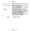
- An address block (4 bytes) indicated by the "lock" of the main memory corresponds to the above-mentioned "lock variable". If the contents are 0, it is indicated that the process is in a lock-release status. If the contents are its own ID (contents of ID to which each process belongs), it is indicated that the process is being locked.
- Fig. 1 the function of each instruction is described on its right side as comments.
- an instruction string structured as shown in Fig. 1 since in a cas instruction, there is always a possibility that an access to the main memory of another processor (store) may occur, the processor always operates to obtain a cache block exclusive right. In this case, a plurality of processors tries to obtain the same lock variable and competition among a plurality of segments of cache becomes tough, which is a problem.
- Fig. 2 of the accompanying drawings shows an example of an instruction string by which this problem is solved.
- the cache is kept in a shared status unless the lock variable is rewritten (as long as a processor that obtained lock maintains the lock). Therefore, there is no above-mentioned cache competition.
- a lock variable such as barrier synchronization, a processor synchronization process (synchronization waiting), general processor synchronization, I/O synchronization, an idle loop and the like.
- Patent References 1, 2 and 3 are known.
- Patent Reference 1 Japanese Patent Laid-open Application No. 3-164964
- Patent Reference 2 Japanese Patent Laid-open Application No. 61-229150
- Patent Reference 3 Japanese Patent Laid-open Application No. 2002-41489
- Patent Reference 1 a mechanism for realizing exclusive control by storing a shared variable in main memory and collectively monitoring processors on the main memory, is disclosed.
- a recent processor with cache memory rewriting in the cache is not promptly reflected on the main memory. More particularly, in a write-back cache method, it usually takes a fairly long time to reflect rewriting. Since in a recent processor with write-through cache, memory latency is very short and reflection loss is long. Accordingly, performance degrades.
- Patent Reference 2 a technology for realizing the exclusive control of shared memory among CPUs by providing an access control signal wire (pin) for the exclusive control among CPUs in addition to a system bus shared by a plurality of the CPUs.
- connection between processors for example, the number of input/output pins of an LSI
- the use of one pin as a data line is more effective in performance improvement than the exclusive use of one pin for the purpose of exclusive control. Otherwise, the deletion of even one pin can contribute to the reduction of CPU manufacturing cost more. Therefore, a method for realizing exclusive control among CPUs without increasing the number of pins, is demanded.
- Patent Reference 3 a synchronous control circuit used to control synchronization between a processor and a co-processor, which are in the relationship between a master and a servant, is disclosed.
- a processor can voluntarily catch the operation status of a co-processor since the processor is in a position to issue instructions to the co-processor.
- each processor does not logically store information about the operation statuses of other processors, it is difficult to apply the technology of Patent Reference 3 in order to solve the above-mentioned problems.
- the above-mentioned problems can be solved by predicting the possibility of the rewriting of a lock variable for the exclusive control of memory access and suspending the processor or thread located in a part where, as previously-proposed, a spin loop occurs due to release waiting.
- a processor can be suspended and resumed by providing both a new load instruction to set the monitor start trigger of a memory block, including a memory block to be loaded (hereinafter called "LOAD-WITH-LOOKUP instruction") and a writing detection function to monitor a memory block, and by executing/releasing a suspense instruction, such as a SUSPEND instruction and the like, in accordance with both the LOAD-WITH-LOOKUP instruction and the detection result of the writing detection function, in order to realize the possibility prediction of the rewriting of a lock variable.
- LOAD-WITH-LOOKUP instruction a memory block to be loaded
- a suspense instruction such as a SUSPEND instruction and the like
- An embodiment of the present invention can also be applied to a co-processor system.
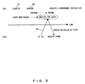
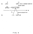
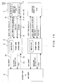
- a CPU 1 issues a LOAD-WITH-LOOKUP instruction after the failed acquisition by CAS [A] and monitors store to lock variable [A] (possibility of release from another CPU 2). Simultaneously, the CPU 1 is entered into a suspense status by a SUSPEND instruction. Then, the CPU 1 can be restored using the detection of the store possibility of the lock variable [A] by another CPU 2 as a trigger, and the re-acquisition of the lock variable [A] can be attempted. Thus, no useless spin loop occurs.
- the CPU 1 starts monitoring a target lock variable [A] by a LOAD-WITH-LOOKUP instruction and then enters into SUSPENSE (suspense status). If the CPU 1 detects an access for the release of the lock variable [A] by the other CPU 2, the CPU 1 is restored from the suspense status and starts executing a subsequent instruction.
- SUSPENSE suspense status
- An embodiment of the present invention analyzes the instruction string of the existing program, predicts the generation area of a spin loop and suspends/resumes the processor. Specifically, the present invention executes the step of detecting an instruction string that will become a spin loop used to detect the possibility of rewriting a lock variable from the existing instruction string and the step of suspending the relevant processor or hardware thread instead of the previously-proposed spin loop.
- an embodiment of the present invention is provided with a writing detection function to monitor and detect the possibility of rewriting a lock variable in cache memory.
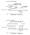
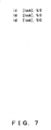
- a memory access instruction as shown in Fig. 7 can be observed in the execution range of several tens of instructions. Even if it is unlucky, it can be observed as shown in Fig. 8.
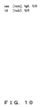
- a common fact is that if two instructions accessing the same address is issued closely, as shown in Fig. 10, when lock acquisition fails, the processor falls into a spin loop.
- a function to detect the approach of these two instructions a function to suspend the instruction when detecting it and a function to start monitoring at the time point of cas and to recognize the rewriting by another system, a method for solving the conventional problems in which LOAD-WITH-LOOKUP and SUSPEND instructions are almost combined, can be obtained.
- FIG. 11 A basic example is shown in Fig. 11. However, it can also be applied to a series of cas instructions to the same address. Alternatively, it can also be applied to a series of 1d instructions to the same address.
- the previously-proposed spin loop can be improved by using the LOAD-WITH-LOOKUP (llkup) instruction of an embodiment of the present invention.
- One of the improvement methods is shown in Fig. 12. Specifically, firstly, a lock variable [lock] is loaded onto a register %10 by an 11kup instruction, and simultaneously the monitor of store possibility of the lock variable [lock] is started. Then, the contents of the register %10 are evaluated by a tst instruction. If the contents are not 0 (another processor obtains its exclusive right), the execution point attempts to be branched to loop:.
- Fig. 13 conceptually shows a configuration of the information processing device executing the control method of the information processing device, which is one preferred embodiment of the present invention.
- the information processing device of the preferred embodiment comprises a plurality of instruction control units 10, a storage device 30 storing data accessed by these instruction control units and cache memory 20 which is inserted between this storage device 30 and each instruction control unit 10, temporarily storing data to be transmitted/received between them and capable of accessing data faster than the storage device 30.
- both the cache memory 20, such as (primary operand) cache and the like, and the storage device 30 as the lower-order memory of the secondary cache, main memory or the like are connected to the instruction control unit 10 as followers.
- the storage device 30 is shared by he plurality of instruction control units 10.
- each instruction control unit 10 is in charge of the interpretation/execution of instructions and operation.
- Each instruction control unit 10 comprises a register.
- Each instruction control unit 10 also issues a memory access instruction 51 and an address 51a to the cache memory 20, outputs store data 52 to be stored to the storage device 30 and inputs fetch data 53 read from the storage device 30 through the cache memory 20.
- This preferred embodiment further comprises a control interface, such as a LOAD-WITH-LOOPUP instruction 54 (hereinafter called "llkup instruction 54"), which is described later, a nullify request 55 to designate the nullification of specific data in the cache memory 20 and the like, as an memory access instruction 51.
- a control interface such as a LOAD-WITH-LOOPUP instruction 54 (hereinafter called "llkup instruction 54"), which is described later, a nullify request 55 to designate the nullification of specific data in the cache memory 20 and the like, as an memory access instruction 51.
- the instruction set 12 of the instruction control unit 10 of this preferred embodiment includes an 11kup instruction 54.
- the instruction set 12 also includes a specific SUSPEND instruction 12a to restore the processor from the suspense status using the detection of a store possibility detection signal 56, which is described later, and a regular SUSPEND instruction 12b to permit its resumption by the conventional offering, which are properly used as requested.
- the cache memory 20 comprises a cache data unit 21 temporarily storing data to be transmitted/received between the instruction control unit 10 and the storage device 30, for example, in units of lines or the like, and a cache tag unit managing data stored in this cache data unit 21.
- a status 22a, an address 22c of the storage device 30, other management information 22d are set for each data storage unit, such as a line in the cache data unit 21.
- the cache memory 20 comprises store monitoring logic 40.
- This store monitoring logic 40 monitors whether data in the cache memory 20, corresponding to the access area of the storage device 30, of the relevant 11kup instruction 54 is rewritten by another instruction control unit 10 different from the instruction control unit 10 that issued the relevant 11kup instruction 54, and transmits a store possibility detection signal 56 to the instruction control unit 10 in response to it.
- the operand cache part of the cache memory 20, such as a primary cache and the like is important, and it can handle the target memory access of a load instruction (fetch instruction) and the like, regardless of which the cache configuration is, unified or separate, that is, whether or not instruction cache and operand cache (data cache) are separated.
- the cache memory 20 can be write-back (store-in) cache or write-through (store-through) cache, here the description is made assuming that the cache memory 20 is write-back cache.
- cache statuses such as MCI (modified, clean and invalid), MESI (modified, exclusive, sharable and invalid), MOEDI (modified, owned, exclusive, sharable and invalid) and the like.
- MCI modified, clean and invalid
- MESI modified, exclusive, sharable and invalid
- MOEDI modified, owned, exclusive, sharable and invalid
- shared (C) shared
- monopolized (M) monopolized
- I invalid
- MESI and MOSEI are obtained simply by adding an auxiliary status to each of them, which are described later with reference to MCI.
- E and M are statuses having an exclusive right
- O and S are shared statuses.
- the cache memory 20 of the execution processor obtains an exclusive right to the relevant memory area when performing store.
- the exclusive right is obtained, the corresponding memory areas of other processors enter into "invalid" statuses.
- a 11kup instruction 54 (LOAD-WITH-LOOKUP instruction 54) is newly set between an instruction control unit 10 and cache memory 20 as described above, according to the basic control principle of this cache memory. Then, if this 11kup instruction 54 is executed, the following control operations are performed.
- the monitoring of a memory area by the store monitoring logic 40 can be realized on a cache tag or a register.
- the cache tag unit 22 is paired with data, and includes a cache status (one of the above-mentioned M, C, I, etc.) indicated by a status 22a, an address 22c and other management information 22d (privilege flag, context, etc.).
- LOOK flag information is provided here.
- the cache tag unit 22 is provided with a LOOK flag 22b for the 11kup instruction 54 for each data storage unit.
- this LOOK flag 22b is not set. If the 11kup instruction 54 is executed, the following load process is performed accompanying the registration the 11kup instruction 54.
- the store possibility of other processors is determined by the nullification of a cache line in which this LOOK flag 22b is set. It is generally determined by the following events.
- the cache method includes several methods, such as a write-through/write-back method in store management, an association method (set associative method for cache hit rate improvement), an address management method (virtually indexed physically tagged (VIPT), physically indexed physically tagged (PIPT)) and the like.
- association method set associative method for cache hit rate improvement
- address management method virtual indexed physically tagged (VIPT), physically indexed physically tagged (PIPT)
- VIPPT virtual indexed physically tagged
- PIPT physically indexed physically tagged
- a register 41 is provided instead of providing the cache tag unit 22 with a LOOK flag 22b, and an address 51a is set by executing the 11kup instruction 54.
- the address is compared with the contents of the set register 41 by a comparator 42, and the output of the AND by a logic control circuit 43, of a comparison result outputted from the comparator 42 and the nullification request 55, is returned to the instruction control unit 10 as a store possibility detection signal 56.
- the spin loop of the instruction control unit 10 can be avoided in exclusive control by the reference /update of a shared variable (lock variable) in the storage device 30.
- an address range can also be set in the register 41. For example, if a target fetch size is an 11kup instruction 54 of four bytes, it can be recorded that the designated address is four bytes. If a plurality of 11kup instructions 54 is executed, the range can be recorded.
- a cache line size is used for the range, for convenience's sake. Even if a cache line size is four-byte fetch, its target address range is regarded to be 64 bytes (there is no problem at all if cache is not shared by a plurality of processors. More particularly it is in a case where the cache is shared by a plurality of processors that a small address range has a meaning).
- a method in which an address range of four bytes can be used such as a global buffer storage (GBS) method, a chip multi-processor (CMP) method and a hardware multi-thread method (a processor that executes one hardware thread in this case is called "logical processor"
- GCS global buffer storage
- CMP chip multi-processor
- logical processor hardware multi-thread method
- a processor that executes one hardware thread in this case is called "logical processor”
- address range determination by store executed by a shared logical processor is added to address matching determination accompanying the above-mentioned nullification.
- a simple method for first of all entering a processor into a suspense status is to generate a SUSPEND instruction to instruct the processor to enter into a suspense status and to execute the instruction. Namely, if there is an instruction, suspense can be realized by interpreting and executing the instruction.
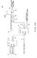
- the clock control system power-saving control unit 60
- Fig. 18 the clock control system
- Fig. 19 the clock control system
- a power-saving control unit 60 is inserted in the supply route of the operation clock 71 to the instruction control unit 10.
- This power-saving control unit 60 comprises a flip-flop circuit 61 using a suspense execution signal 57 from the instruction control unit 10 and a store possibility detection signal 56 from the store monitoring logic 40 of the cache memory 230 as set input (SET) and reset input (RESET), respectively, and an AND circuit 63 generating an operation clock 71a by the AND of a signal obtained logically inverting the Q output of the flip-flop circuit 61 by a logic inversion circuit 62, and the operation clock 71, and inputting the clock to the instruction control unit 10.
- SET set input
- REET reset input
- the clock supply of the execution control unit can be suspended at the time of suspense, and the clock supply can be resumed at the time of the detection of store possibility.
- the existing suspense/resumption methods can be combined.
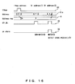
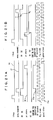
- the power-saving control unit 60A shown in Fig. 20 and the timing chart shown in Fig. 21 realize this.
- both a flip-flop circuit 66 using the execution signal of the 11kup instruction 54 as the suspense execution signal 57 as set input (SET) and reset input (RESET), respectively, and a logic inversion circuit 67 inverting the Q output of the flip-flop circuit 66 are disposed in the reset input route of the flip-flop circuit 61 shown in Fig. 18. Furthermore, both a logic inversion circuit 64 inverting the Q output of the flip-flop circuit 61 and an AND circuit 65 calculating the AND of the output of the logic inversion circuit 64 and a suspense during-execution signal 57a which always becomes true during suspense execution are inserted between the flip-flop circuit 61 and logic inversion circuit 62.
- a store possibility detection signal 56 is regularly detected after suspense execution as shown in Fig. 21A, the input of the operation clock 71a to the instruction control unit 10 is suspended during suspense execution. However, if a store possibility detection signal 56 is detected before suspense execution as shown in Fig. 21B, the input of the operation clock 71a to the instruction control unit 10 is not suspended during suspense execution and the instruction control unit 10 continues to operate.
- the Q output of the flip-flop circuit 61 can be used as an early store detection signal 68 for detecting that a store possibility detection signal 56 was detected before suspense execution, as requested.
- the useless power consumption due to the idle-running waiting of the instruction control unit 10, such as the conventional spin loop can be avoided by monitoring the change of a shared variable for exclusive control due to the access of another instruction control unit 10, using the issuance of an 11kup instruction 54 as a trigger, and also entering the instruction control unit 10 into a suspense (operation clock suspense) status by a special suspend instruction 12a and restoring the instruction control unit 10 using the input to the power-saving control unit 60 of a store possibility detection signal 56 as a trigger, if the change of the shared variable is anticipated.
- a suspense operation clock suspense
- the idle-running waiting of each logical processor means the suspense of other processors sharing the hardware. Therefore, the application of the technology of this preferred embodiment, for precisely suspending a processor that falls into an idle-running waiting status can contribute not only to power saving but also to the effective utilization of the throughput (resources) of each logical processor.
- an embodiment of the present invention is applied to a processor corresponding to a hardware multi-thread, improving throughput by pretending as if a plurality of logical processors were mounted on one physical chip, not only power saving but also the effective utilization of processor throughput (processor resources) can be realized.
- VMT vertical multi-thread
- a thread logical processor
- SMT simultaneous multi-thread
- the spin loop discrimination unit 80 comprises a register 81 storing an address 51a accompanying a memory access instruction 51, an OR circuit 82 calculating the OR of a load instruction detection signal 58a outputted from the decoding unit 11 of the instruction control unit 10 and a compare/swap instruction detection signal 58c, a comparator 83 comparing the stored contents of the register 81 with the address 51a, an AND circuit 87 calculating the AND of the output of the comparator 83 and the output of the OR circuit 82 and outputting the AND as a spin detection signal 87a, a logic inversion circuit 84 inverting the output of the comparator 83, an AND circuit 85 calculating the AND of the output of the logic inversion circuit 84 and the output of the OR circuit 82, an OR circuit 86 calculating the OR of the output of the AND circuit 85 and the store instruction detection signal 58b of the decoding unit 11 and outputting the OR as a spin release signal 86a, and a counter 88 which is counted up by the spin
- the address 51a is taken in the register 81 when a compare/swap instruction detection signal 58c is detected. Then, if the contents of the register 81 coincide with the address 51a accompanying the load instruction when the load instruction detection signal 58a is detected, the spin detection signal 87a is outputted. If the address 51a does not coincide with the contents of the register 81 at the time of the detection of the store instruction detection signal 58b or at the time of the detection of the load instruction detection signal 58a or a compare/swap instruction detection signal 58c, the spin release signal 86a is outputted.
- the counter 88 is counted up by the spin detection signal 87a, and if the count reaches a specific value (1 acceptable), the then ld/cas instruction is regarded to be equivalent to an 11kup instruction. If the counting continues and the count exceeds the specific value, the processor is suspended after the then ld/cas instruction is completed. If the spin release signal 86a is detected, mis-detection can be suppressed by resetting the counter 88. Once the processor is suspended, the counter 88 is reset. Otherwise, when restoring from the suspense, the processor promptly enters into the next suspense status.
- a spin loop discrimination unit 80 By providing such a spin loop discrimination unit 80, a spin loop can be detected regardless of whether or not an 11kup instruction 54 is mounted. Power saving can also controlled regardless of whether or not there is a suspend instruction.
- the bad influence on other thread processes of a processor core can be eliminated by removing the useless idle running of a spin loop.
- porting software to a processor provided with a LOAD-WITH-LOOKUP instruction a program written in the existing instruction codes can be easily rewritten, and accordingly the porting cost of software can be suppressed.
- the waste of both power consumption and processor resources which are due to a spin loop for exclusive control among a plurality of logical or physical processors can be reduced.
- one physical processor core is provided with a plurality of hardware threads and which can operate as if it were provided with a plurality of logical processors
- the performance degradation of other logical processors due to the spin loop of one logical processor can also be prevented.
- the present invention is expressed as follows from a different viewpoint.
- a method and architecture for monitoring memory blocks including a memory block to be loaded in an instruction set architecture having a load instruction to read a value from main memory mounted on an information processing device with cache memory.
- a method and architecture with a load instruction (LOAD-WITH- LOOKUP instruction) with a function to monitor memory blocks including a memory block to be loaded.
- a method and a device for providing the detection means more particularly a cache tag, set forth in note 3, with a flag indicating a during-monitor status and monitoring a cache line with the flag.
- a method and a device for providing the detection means more particularly one or more registers, setting a monitor address and monitoring by checking an address range, based on this set address.
- a process method and a device with cache memory for storing the data of an address to be monitored by the cache as the detection means set forth in note 3, in the cache, and determining store possibility when receiving a cache line nullify instruction (Buffer Invalidate or Copy-back and invalidate).
- a process method and a device with cache memory for storing the data of an address to be monitored by the cache as the detection means set forth in note 3, in the cache, and determining store possibility when there is replacement.
- a logical processor logical CPU
- the method and device according to note 8 for preventing the processor from resumption by address monitor by providing a means for instructing the SUSPEND instruction not to monitor an address in order to temporarily suspend without address monitor.
- a store possibility detection means with a mechanism for detecting a case where a specific logical processor writes data in the memory block monitoring range set forth in note 2, of shared cache in a configuration where one segment of cache can be shared by a plurality of logical processors, such as shared cache (GBS method), a processor in which one physical chip includes a plurality of processor cores (CMP method) and a processor in which one physical processor core is provided with a plurality of hardware threads (strand) and which can operate as if there were a plurality of logical processors (such as, MT method, HMT, SMT, VMT, etc.).
- GSS method shared cache
- CMP method processor in which one physical processor core is provided with a plurality of hardware threads (strand) and which can operate as if there were a plurality of logical processors (such as, MT method, HMT, SMT, VMT, etc.).
- the method and device which operates regarding the set of a fetch/store instruction to operate the same address block (such as a cas instruction, an instruction to atomically load data from memory and store memory) and a load instruction as an monitor/suspend instruction, instead of the LOAD-WITH-LOOKUP/SUSPEND instruction set forth in note 2 (can also be provided).
- a fetch/store instruction such as a cas instruction, an instruction to atomically load data from memory and store memory
- a load instruction as an monitor/suspend instruction
Landscapes
- Engineering & Computer Science (AREA)
- Software Systems (AREA)
- Theoretical Computer Science (AREA)
- Physics & Mathematics (AREA)
- General Engineering & Computer Science (AREA)
- General Physics & Mathematics (AREA)
- Memory System Of A Hierarchy Structure (AREA)
- Executing Machine-Instructions (AREA)
- Power Sources (AREA)
- Advance Control (AREA)
Abstract
Description
Patent Reference 1: Japanese Patent Laid-open Application No. 3-164964
Patent Reference 2: Japanese Patent Laid-open Application No. 61-229150
Patent Reference 3: Japanese Patent Laid-open Application No. 2002-41489
- 1. Execution of an 11kup instruction through monitor start
- 2. Detection of store possibility
- 3. Execution of a SUSPEND instruction
Claims (22)
- A method for controlling a processor (10) which accesses information of a storage device (30) through cache memory (20), comprising:a first step of reading information stored in a target address or an address range of the storage device (30) and monitoring whether there is an update access to the address or the address range from another processor (10);a second step of entering the processor (10) into a suspense status; anda third step of releasing the suspense status using the occurrence of the update access as a trigger.
- The processor control method according to claim 1, wherein
if the occurrence of the update access is detected between said first and second steps, the execution of said second step is suppressed. - The processor control method according to claim 1 or 2, wherein
part of cache management information (22) for managing the cache memory (20) comprises discrimination information for discriminating the storage area of the cache memory (20) corresponding to the specific storage area of the storage device (30), and
in said first step the storage area of the cache memory (20), corresponding to the address or address range of the storage device (30) accessed is designated as a monitor target by attaching the discrimination information, and
in said third step the suspense status is released using the occurrence of the nullification or rewriting of the information about the storage area of the cache memory (20) as a trigger. - The processor control method according to claim 1, 2 or 3, wherein
in said second step, the clock supply to the processor (10) is suspended, and
in said third step, the clock supply is resumed. - A method for controlling a processor which accesses information of a storage device (30) through cache memory (20), comprising:a first step of detecting an instruction string composed of at least one of a first instruction to collectively read and update information in a target address or an address range of the storage device (30) and a second instruction to read information about the address or address range;a second step of monitoring whether there is an update access to the address or the address range from another processor (10) and also entering the processor (10) into a suspense status using detection of the instruction string as a trigger; anda third step of releasing the suspense status using the occurrence of the update access to the address or address range from another processor (10) as a trigger.
- The processor control method according to claim 5, wherein
part of cache management information (22) for managing the cache memory (20) comprises discrimination information for discriminating the storage area of the cache memory (20) corresponding to the specific storage area of the storage device (30), and
in the first step, the storage area of the cache memory (20), corresponding to the address or address range of the storage device (30) accessed is designated as a monitor target by attaching the discrimination information, and
in said third step, the suspense status is released using the occurrence of the nullification or rewriting of the information about the storage area of the cache memory (20) as a trigger. - The processor control method according to claim 5 or 6, wherein
in said second step, the clock supply to the processor (10) is suspended, and
in said third step, the clock supply is resumed. - An information processing device, comprising:an instruction control unit (10);cache memory (20) inserted between the instruction control unit (10) and a storage device (30);a load instruction to read information from the storage device (30) into the instruction control unit (10); anda monitor trigger setting function to set the monitor start trigger of a specific storage area of the storage device (30), including a target access area of the load instruction.
- An information processing device, comprising:an instruction control unit (10);cache memory (20) inserted between the instruction control unit (10) and a storage device (30);a load instruction to read information from the storage device (30) into the instruction control unit (10); anda writing detection function (40) to monitor a specific storage area of the storage device (30), including a target access area of the load instruction and to detect a possibility that information may be written into the specific storage area.
- The information processing device according to claim 9, wherein
part of cache management information (22) for managing said cache memory (20) comprises discrimination information for discriminating the storage area of said cache memory (20) corresponding to the specific storage area of the storage device (30), and the storage area of the cache memory (20), to which the discrimination information is attached, is designated as the monitor target of said writing detection function (40). - The information processing device according to claim 9 or 10, wherein
said writing detection function (40) comprises at least one register (41), and
a monitor address indicating the specific storage area is set in said register (41), and the specific storage area is monitored by comparing the monitor address with an access address to all segments of cache memory (20). - The information processing device according to claim 9, 10 or 11, wherein
if there is an instruction to nullify or rewrite information stored corresponding to the specific storage area of said cache memory (20) , it is determined that there is a possibility of writing into the specific storage area. - An information processing device, comprising:an instruction control unit (10);cache memory (20) inserted between the instruction control unit (10) and a storage device (30);a load instruction to read information from the storage device (30) into the instruction control unit (10); anda suspense instruction (12a) to enter the instruction control unit (10) into a suspense status and to release the suspense status using detection of a possibility of writing the information into the specific storage area of the storage device (30), including a target access area of the load instruction as a trigger.
- The information processing device according to claim 13, further comprising
a clock supply control function (60) to suspend and resume clock supply to said instruction control unit (10) in synchronization with entry to the suspense status by said suspense instruction and release from the suspense status. - An information processing device provided with an exclusive control mechanism for exclusively controlling access to shared memory of a plurality of instruction control units (10) by rewriting specific information in a specific area of the shared memory, comprising
a clock supply control function (60) to suspend clock supply to the relevant instruction control unit (10) while one of the plurality of instruction control units (10) is waiting for rewriting of the specific information by another instruction control unit (10) as a trigger. - An information processing device, comprising
a plurality of logical or physical instruction control units (10);
cache memory (20) which is inserted between each of the instruction control unit (10) and a storage device (30) and is shared by the plurality of instruction control units (10); and
a writing detection function (40) to notify other instruction control units (10) of a fact that one of the plurality of instruction control units (10) has written information into a specific storage area of the storage device (30). - The information processing device according to claim 16, wherein
each of said instruction control units (10) comprises
a suspense instruction to enter the relevant instruction control unit (10) into a suspense status and to release the suspense status using notification from said writing detection function (40) as a trigger. - A processor (10) with an instruction set, said instruction set comprising:a load instruction to access a storage device (30) through cache memory (20) and to read information from the storage device (30); anda specific instruction (54) to set the existence/non-existence of writing in a specific storage area of the storage device (30), including a target access area of the load instruction as a monitor start trigger.
- An information processing device which accesses information of a storage device (30) through cache memory (20), comprising:a first function to detect an instruction string composed of at least one of a first instruction to collectively read and update information in a target address or address range of the storage device (30) and a second instruction to read information about the address or address range; anda second function to monitor whether there is an update access to the address or address range from another processor (10) and also to enter the information processing device into a suspense status, using detection of the instruction string as a trigger ; anda third function to release the suspense status using the occurrence of the update access to the address or address range from another processor (10) as a trigger.
- Cache memory (20) which is inserted between an instruction control unit (10) and a storage device (30) and temporarily stores information transmitted/received between the storage device (30) and the instruction control unit (10), comprising
a writing detection function (40) to detect a possibility that information may be written into the specific storage area of the storage device (30), including a target access area of a load instruction to read the information from the storage device (30) into the instruction control unit (10). - The cache memory (20) according to claim 20, wherein
part of cache management information (22) for managing said cache memory (20) comprises discrimination information (22b) for discriminating the storage area of said cache memory (20) corresponding to the specific storage area of the storage device (30) , and the storage area of the cache memory (20), to which the discrimination information is attached, is designated as the monitor target of said writing detection function (40). - The cache memory (20) according to claim 20 or 21, wherein
said writing detection function (40) comprises at least one register (41), and
a monitor address indicating the specific storage area is set in said register (41), and the specific storage area is monitored by comparing the monitor address with an access address to all segments of cache memory (20).
Applications Claiming Priority (2)
| Application Number | Priority Date | Filing Date | Title |
|---|---|---|---|
| JP2004135875 | 2004-04-30 | ||
| JP2004135875A JP4376692B2 (en) | 2004-04-30 | 2004-04-30 | Information processing device, processor, processor control method, information processing device control method, cache memory |
Publications (2)
| Publication Number | Publication Date |
|---|---|
| EP1594059A2 true EP1594059A2 (en) | 2005-11-09 |
| EP1594059A3 EP1594059A3 (en) | 2007-09-05 |
Family
ID=34930647
Family Applications (1)
| Application Number | Title | Priority Date | Filing Date |
|---|---|---|---|
| EP04255531A Withdrawn EP1594059A3 (en) | 2004-04-30 | 2004-09-13 | Information processing devices and control methods therefor |
Country Status (3)
| Country | Link |
|---|---|
| US (1) | US7853756B2 (en) |
| EP (1) | EP1594059A3 (en) |
| JP (1) | JP4376692B2 (en) |
Cited By (3)
| Publication number | Priority date | Publication date | Assignee | Title |
|---|---|---|---|---|
| EP1857927A3 (en) * | 2006-05-17 | 2008-06-11 | Intel Corporation | Method and system for enhanced thread synchronization and coordination |
| GB2495183A (en) * | 2011-09-02 | 2013-04-03 | Nvidia Corp | Putting a processor in to a low power state while it is in a spinlock state. |
| US9733937B2 (en) | 2004-06-30 | 2017-08-15 | Intel Corporation | Compare and exchange operation using sleep-wakeup mechanism |
Families Citing this family (26)
| Publication number | Priority date | Publication date | Assignee | Title |
|---|---|---|---|---|
| US7213093B2 (en) * | 2003-06-27 | 2007-05-01 | Intel Corporation | Queued locks using monitor-memory wait |
| US7302543B2 (en) * | 2004-06-16 | 2007-11-27 | Nec Laboratories America, Inc. | Compressed memory architecture for embedded systems |
| JP4287799B2 (en) * | 2004-07-29 | 2009-07-01 | 富士通株式会社 | Processor system and thread switching control method |
| US8936057B2 (en) * | 2005-08-30 | 2015-01-20 | Rockwell Collins, Inc. | Substrate lamination system and method |
| US7395418B1 (en) * | 2005-09-22 | 2008-07-01 | Sun Microsystems, Inc. | Using a transactional execution mechanism to free up processor resources used by a busy-waiting thread |
| US7487279B2 (en) * | 2007-01-23 | 2009-02-03 | International Business Machines Corporation | Achieving both locking fairness and locking performance with spin locks |
| JP5270924B2 (en) * | 2008-01-30 | 2013-08-21 | 株式会社東芝 | Fixed-length memory block management apparatus and control method for fixed-length memory block management apparatus |
| CN101661438B (en) * | 2008-08-29 | 2013-08-28 | 鸿富锦精密工业(深圳)有限公司 | Electronic device and method for expanding addressing space of central processing unit |
| US8156275B2 (en) * | 2009-05-13 | 2012-04-10 | Apple Inc. | Power managed lock optimization |
| JP5590032B2 (en) * | 2009-06-30 | 2014-09-17 | 富士通株式会社 | Computer apparatus and parallel computer system |
| US8464035B2 (en) * | 2009-12-18 | 2013-06-11 | Intel Corporation | Instruction for enabling a processor wait state |
| JP2011150422A (en) | 2010-01-19 | 2011-08-04 | Renesas Electronics Corp | Data processor |
| KR101641541B1 (en) * | 2010-03-31 | 2016-07-22 | 삼성전자주식회사 | Apparatus and method of dynamically distributing load in multi-core |
| KR101664108B1 (en) * | 2010-04-13 | 2016-10-11 | 삼성전자주식회사 | Apparatus and method of hardware acceleration for processing synchronization of multi core |
| KR101959567B1 (en) * | 2012-05-14 | 2019-03-18 | 에스케이하이닉스 주식회사 | non-volatile memory device and method of programming the same |
| US9218289B2 (en) * | 2012-08-06 | 2015-12-22 | Qualcomm Incorporated | Multi-core compute cache coherency with a release consistency memory ordering model |
| CN103885892A (en) * | 2012-12-20 | 2014-06-25 | 株式会社东芝 | Memory controller |
| CN104956274B (en) * | 2013-01-30 | 2016-11-09 | 三菱电机株式会社 | Numerical control device |
| GB2514618B (en) * | 2013-05-31 | 2020-11-11 | Advanced Risc Mach Ltd | Data processing systems |
| JP6221792B2 (en) * | 2014-02-05 | 2017-11-01 | 富士通株式会社 | Information processing apparatus, information processing system, and information processing system control method |
| US9619386B2 (en) | 2015-01-29 | 2017-04-11 | Kabushiki Kaisha Toshiba | Synchronization variable monitoring device, processor, and semiconductor apparatus |
| US10185564B2 (en) * | 2016-04-28 | 2019-01-22 | Oracle International Corporation | Method for managing software threads dependent on condition variables |
| JPWO2018150524A1 (en) * | 2017-02-16 | 2020-02-20 | オスカーテクノロジー株式会社 | Processor system and multiprocessor system |
| US11086672B2 (en) * | 2019-05-07 | 2021-08-10 | International Business Machines Corporation | Low latency management of processor core wait state |
| US11113194B2 (en) * | 2019-09-04 | 2021-09-07 | Xilinx, Inc. | Producer-to-consumer active direct cache transfers |
| US12353331B2 (en) * | 2023-09-29 | 2025-07-08 | Hewlett Packard Enterprise Development Lp | Kernel memory monitor for user-space mapping change notifications |
Family Cites Families (25)
| Publication number | Priority date | Publication date | Assignee | Title |
|---|---|---|---|---|
| US4513367A (en) | 1981-03-23 | 1985-04-23 | International Business Machines Corporation | Cache locking controls in a multiprocessor |
| US4780843A (en) * | 1983-11-07 | 1988-10-25 | Motorola, Inc. | Wait mode power reduction system and method for data processor |
| JPS61229150A (en) | 1985-04-04 | 1986-10-13 | Mitsubishi Electric Corp | System for controlling access to shared memory |
| JPH0381859A (en) | 1989-08-25 | 1991-04-08 | Nec Corp | Multiprocessor system |
| JPH03164964A (en) | 1989-11-24 | 1991-07-16 | Nippon Telegr & Teleph Corp <Ntt> | Exclusive control processor for information processor |
| JP2708943B2 (en) * | 1990-08-08 | 1998-02-04 | 三菱電機株式会社 | Cache memory controller |
| JP2963257B2 (en) | 1991-11-01 | 1999-10-18 | 富士通株式会社 | Processing equipment |
| JPH05225149A (en) | 1992-02-13 | 1993-09-03 | Toshiba Corp | Lock method |
| JPH0659982A (en) * | 1992-08-10 | 1994-03-04 | Hitachi Ltd | Method and device for controlling virtual storage |
| JP3164964B2 (en) | 1994-03-23 | 2001-05-14 | 株式会社ソディック | Wire electric discharge machining method and power supply circuit for wire electric discharge machining |
| JP3546694B2 (en) | 1998-03-31 | 2004-07-28 | 日本電気株式会社 | Multi-thread computer system and multi-thread execution control method |
| US6189088B1 (en) * | 1999-02-03 | 2001-02-13 | International Business Machines Corporation | Forwarding stored dara fetched for out-of-order load/read operation to over-taken operation read-accessing same memory location |
| US6360364B1 (en) * | 1999-03-17 | 2002-03-19 | Microsoft Corporation | System and method for installing an application on a portable computer |
| US6493741B1 (en) * | 1999-10-01 | 2002-12-10 | Compaq Information Technologies Group, L.P. | Method and apparatus to quiesce a portion of a simultaneous multithreaded central processing unit |
| US6802039B1 (en) * | 2000-06-30 | 2004-10-05 | Intel Corporation | Using hardware or firmware for cache tag and data ECC soft error correction |
| JP2002041489A (en) | 2000-07-25 | 2002-02-08 | Mitsubishi Electric Corp | Synchronous signal generation circuit, processor system using the same, and synchronous signal generation method |
| US6836824B1 (en) * | 2000-09-26 | 2004-12-28 | Sun Microsystems, Inc. | Method and apparatus for reducing power consumption in a cache memory system |
| US6877088B2 (en) * | 2001-08-08 | 2005-04-05 | Sun Microsystems, Inc. | Methods and apparatus for controlling speculative execution of instructions based on a multiaccess memory condition |
| WO2003040948A1 (en) | 2001-11-08 | 2003-05-15 | Fujitsu Limited | Computer and control method |
| US6986015B2 (en) * | 2001-12-10 | 2006-01-10 | Incipient, Inc. | Fast path caching |
| US7363474B2 (en) * | 2001-12-31 | 2008-04-22 | Intel Corporation | Method and apparatus for suspending execution of a thread until a specified memory access occurs |
| US7127561B2 (en) * | 2001-12-31 | 2006-10-24 | Intel Corporation | Coherency techniques for suspending execution of a thread until a specified memory access occurs |
| JP4252301B2 (en) * | 2002-12-26 | 2009-04-08 | 株式会社日立製作所 | Storage system and data backup method thereof |
| US7120775B2 (en) * | 2003-12-29 | 2006-10-10 | Intel Corporation | Inter-procedural allocation of stacked registers for a processor |
| US7349999B2 (en) * | 2003-12-29 | 2008-03-25 | Intel Corporation | Method, system, and program for managing data read operations on network controller with offloading functions |
-
2004
- 2004-04-30 JP JP2004135875A patent/JP4376692B2/en not_active Expired - Fee Related
- 2004-09-10 US US10/937,253 patent/US7853756B2/en not_active Expired - Fee Related
- 2004-09-13 EP EP04255531A patent/EP1594059A3/en not_active Withdrawn
Cited By (5)
| Publication number | Priority date | Publication date | Assignee | Title |
|---|---|---|---|---|
| US9733937B2 (en) | 2004-06-30 | 2017-08-15 | Intel Corporation | Compare and exchange operation using sleep-wakeup mechanism |
| EP1857927A3 (en) * | 2006-05-17 | 2008-06-11 | Intel Corporation | Method and system for enhanced thread synchronization and coordination |
| GB2495183A (en) * | 2011-09-02 | 2013-04-03 | Nvidia Corp | Putting a processor in to a low power state while it is in a spinlock state. |
| GB2495183B (en) * | 2011-09-02 | 2013-09-11 | Nvidia Corp | Method for power optimized multi-processor synchronization |
| US8713262B2 (en) | 2011-09-02 | 2014-04-29 | Nvidia Corporation | Managing a spinlock indicative of exclusive access to a system resource |
Also Published As
| Publication number | Publication date |
|---|---|
| JP2005316854A (en) | 2005-11-10 |
| JP4376692B2 (en) | 2009-12-02 |
| EP1594059A3 (en) | 2007-09-05 |
| US20050246506A1 (en) | 2005-11-03 |
| US7853756B2 (en) | 2010-12-14 |
Similar Documents
| Publication | Publication Date | Title |
|---|---|---|
| US7853756B2 (en) | Information processing device, processor, processor control method, information processing device control method and cache memory | |
| US12498931B2 (en) | Preserving memory ordering between offloaded instructions and non-offloaded instructions | |
| US7836260B2 (en) | Low complexity speculative multithreading system based on unmodified microprocessor core | |
| US9507647B2 (en) | Cache as point of coherence in multiprocessor system | |
| US8185700B2 (en) | Enabling speculative state information in a cache coherency protocol | |
| US8099556B2 (en) | Cache miss detection in a data processing apparatus | |
| US9146844B2 (en) | Apparatus, method, and system for providing a decision mechanism for conditional commits in an atomic region | |
| US7500087B2 (en) | Synchronization of parallel processes using speculative execution of synchronization instructions | |
| CN101203831B (en) | Apparatus, method and system for caching memory updates | |
| US10019263B2 (en) | Reordered speculative instruction sequences with a disambiguation-free out of order load store queue | |
| US10592300B2 (en) | Method and system for implementing recovery from speculative forwarding miss-predictions/errors resulting from load store reordering and optimization | |
| US20110208921A1 (en) | Inverted default semantics for in-speculative-region memory accesses | |
| EP1612661A2 (en) | Compare-and-exchange operation using sleep-wakeup mechanism | |
| US5440750A (en) | Information processing system capable of executing a single instruction for watching and waiting for writing of information for synchronization by another processor | |
| KR101355496B1 (en) | Scheduling mechanism of a hierarchical processor including multiple parallel clusters | |
| JP4487744B2 (en) | Multi-thread control device and control method | |
| US20040123078A1 (en) | Method and apparatus for processing a load-lock instruction using a scoreboard mechanism | |
| US7975129B2 (en) | Selective hardware lock disabling | |
| Torrellas | Thread-level speculation | |
| CN120508530A (en) | Dynamic reconfiguration of unified core processor to multi-core processor | |
| CN120508531A (en) | Dynamic reconfiguration of multi-core processor to unified core | |
| Update | Intel® Itanium® Architecture Software Developer’s Manual Rev 2.3 |
Legal Events
| Date | Code | Title | Description |
|---|---|---|---|
| PUAI | Public reference made under article 153(3) epc to a published international application that has entered the european phase |
Free format text: ORIGINAL CODE: 0009012 |
|
| AK | Designated contracting states |
Kind code of ref document: A2 Designated state(s): AT BE BG CH CY CZ DE DK EE ES FI FR GB GR HU IE IT LI LU MC NL PL PT RO SE SI SK TR |
|
| AX | Request for extension of the european patent |
Extension state: AL HR LT LV MK |
|
| PUAL | Search report despatched |
Free format text: ORIGINAL CODE: 0009013 |
|
| AK | Designated contracting states |
Kind code of ref document: A3 Designated state(s): AT BE BG CH CY CZ DE DK EE ES FI FR GB GR HU IE IT LI LU MC NL PL PT RO SE SI SK TR |
|
| AX | Request for extension of the european patent |
Extension state: AL HR LT LV MK |
|
| AKX | Designation fees paid | ||
| REG | Reference to a national code |
Ref country code: DE Ref legal event code: 8566 |
|
| STAA | Information on the status of an ep patent application or granted ep patent |
Free format text: STATUS: THE APPLICATION IS DEEMED TO BE WITHDRAWN |
|
| 18D | Application deemed to be withdrawn |
Effective date: 20080306 |