EP1589789A1 - Organic electroluminescence device - Google Patents
Organic electroluminescence device Download PDFInfo
- Publication number
- EP1589789A1 EP1589789A1 EP04702427A EP04702427A EP1589789A1 EP 1589789 A1 EP1589789 A1 EP 1589789A1 EP 04702427 A EP04702427 A EP 04702427A EP 04702427 A EP04702427 A EP 04702427A EP 1589789 A1 EP1589789 A1 EP 1589789A1
- Authority
- EP
- European Patent Office
- Prior art keywords
- phenanthrolin
- light emitting
- hole transporting
- group
- layer
- Prior art date
- Legal status (The legal status is an assumption and is not a legal conclusion. Google has not performed a legal analysis and makes no representation as to the accuracy of the status listed.)
- Granted
Links
- LIEMXEGURXNQGM-UHFFFAOYSA-N c(cc1)ccc1-c1nc(-c2ccccc2)cc(-c(cc2)ccc2-[n]2c3ccccc3c3ccccc23)c1 Chemical compound c(cc1)ccc1-c1nc(-c2ccccc2)cc(-c(cc2)ccc2-[n]2c3ccccc3c3ccccc23)c1 LIEMXEGURXNQGM-UHFFFAOYSA-N 0.000 description 1
Classifications
-
- H—ELECTRICITY
- H05—ELECTRIC TECHNIQUES NOT OTHERWISE PROVIDED FOR
- H05B—ELECTRIC HEATING; ELECTRIC LIGHT SOURCES NOT OTHERWISE PROVIDED FOR; CIRCUIT ARRANGEMENTS FOR ELECTRIC LIGHT SOURCES, IN GENERAL
- H05B33/00—Electroluminescent light sources
- H05B33/12—Light sources with substantially two-dimensional [2D] radiating surfaces
- H05B33/14—Light sources with substantially two-dimensional [2D] radiating surfaces characterised by the chemical or physical composition or the arrangement of the electroluminescent material, or by the simultaneous addition of the electroluminescent material in or onto the light source
-
- C—CHEMISTRY; METALLURGY
- C09—DYES; PAINTS; POLISHES; NATURAL RESINS; ADHESIVES; COMPOSITIONS NOT OTHERWISE PROVIDED FOR; APPLICATIONS OF MATERIALS NOT OTHERWISE PROVIDED FOR
- C09K—MATERIALS FOR MISCELLANEOUS APPLICATIONS, NOT PROVIDED FOR ELSEWHERE
- C09K11/00—Luminescent materials, e.g. electroluminescent or chemiluminescent
- C09K11/06—Luminescent materials, e.g. electroluminescent or chemiluminescent containing organic luminescent materials
-
- H—ELECTRICITY
- H05—ELECTRIC TECHNIQUES NOT OTHERWISE PROVIDED FOR
- H05B—ELECTRIC HEATING; ELECTRIC LIGHT SOURCES NOT OTHERWISE PROVIDED FOR; CIRCUIT ARRANGEMENTS FOR ELECTRIC LIGHT SOURCES, IN GENERAL
- H05B33/00—Electroluminescent light sources
- H05B33/12—Light sources with substantially two-dimensional [2D] radiating surfaces
- H05B33/26—Light sources with substantially two-dimensional [2D] radiating surfaces characterised by the composition or arrangement of the conductive material used as an electrode
-
- H—ELECTRICITY
- H10—SEMICONDUCTOR DEVICES; ELECTRIC SOLID-STATE DEVICES NOT OTHERWISE PROVIDED FOR
- H10K—ORGANIC ELECTRIC SOLID-STATE DEVICES
- H10K50/00—Organic light-emitting devices
- H10K50/10—OLEDs or polymer light-emitting diodes [PLED]
- H10K50/11—OLEDs or polymer light-emitting diodes [PLED] characterised by the electroluminescent [EL] layers
-
- H—ELECTRICITY
- H10—SEMICONDUCTOR DEVICES; ELECTRIC SOLID-STATE DEVICES NOT OTHERWISE PROVIDED FOR
- H10K—ORGANIC ELECTRIC SOLID-STATE DEVICES
- H10K50/00—Organic light-emitting devices
- H10K50/10—OLEDs or polymer light-emitting diodes [PLED]
- H10K50/14—Carrier transporting layers
-
- H—ELECTRICITY
- H10—SEMICONDUCTOR DEVICES; ELECTRIC SOLID-STATE DEVICES NOT OTHERWISE PROVIDED FOR
- H10K—ORGANIC ELECTRIC SOLID-STATE DEVICES
- H10K85/00—Organic materials used in the body or electrodes of devices covered by this subclass
- H10K85/30—Coordination compounds
- H10K85/321—Metal complexes comprising a group IIIA element, e.g. Tris (8-hydroxyquinoline) gallium [Gaq3]
- H10K85/324—Metal complexes comprising a group IIIA element, e.g. Tris (8-hydroxyquinoline) gallium [Gaq3] comprising aluminium, e.g. Alq3
-
- H—ELECTRICITY
- H10—SEMICONDUCTOR DEVICES; ELECTRIC SOLID-STATE DEVICES NOT OTHERWISE PROVIDED FOR
- H10K—ORGANIC ELECTRIC SOLID-STATE DEVICES
- H10K85/00—Organic materials used in the body or electrodes of devices covered by this subclass
- H10K85/60—Organic compounds having low molecular weight
- H10K85/631—Amine compounds having at least two aryl rest on at least one amine-nitrogen atom, e.g. triphenylamine
-
- H—ELECTRICITY
- H10—SEMICONDUCTOR DEVICES; ELECTRIC SOLID-STATE DEVICES NOT OTHERWISE PROVIDED FOR
- H10K—ORGANIC ELECTRIC SOLID-STATE DEVICES
- H10K85/00—Organic materials used in the body or electrodes of devices covered by this subclass
- H10K85/60—Organic compounds having low molecular weight
- H10K85/631—Amine compounds having at least two aryl rest on at least one amine-nitrogen atom, e.g. triphenylamine
- H10K85/636—Amine compounds having at least two aryl rest on at least one amine-nitrogen atom, e.g. triphenylamine comprising heteroaromatic hydrocarbons as substituents on the nitrogen atom
-
- H—ELECTRICITY
- H10—SEMICONDUCTOR DEVICES; ELECTRIC SOLID-STATE DEVICES NOT OTHERWISE PROVIDED FOR
- H10K—ORGANIC ELECTRIC SOLID-STATE DEVICES
- H10K85/00—Organic materials used in the body or electrodes of devices covered by this subclass
- H10K85/60—Organic compounds having low molecular weight
- H10K85/649—Aromatic compounds comprising a hetero atom
- H10K85/654—Aromatic compounds comprising a hetero atom comprising only nitrogen as heteroatom
-
- H—ELECTRICITY
- H10—SEMICONDUCTOR DEVICES; ELECTRIC SOLID-STATE DEVICES NOT OTHERWISE PROVIDED FOR
- H10K—ORGANIC ELECTRIC SOLID-STATE DEVICES
- H10K85/00—Organic materials used in the body or electrodes of devices covered by this subclass
- H10K85/60—Organic compounds having low molecular weight
- H10K85/649—Aromatic compounds comprising a hetero atom
- H10K85/657—Polycyclic condensed heteroaromatic hydrocarbons
-
- H—ELECTRICITY
- H10—SEMICONDUCTOR DEVICES; ELECTRIC SOLID-STATE DEVICES NOT OTHERWISE PROVIDED FOR
- H10K—ORGANIC ELECTRIC SOLID-STATE DEVICES
- H10K2101/00—Properties of the organic materials covered by group H10K85/00
- H10K2101/10—Triplet emission
-
- H—ELECTRICITY
- H10—SEMICONDUCTOR DEVICES; ELECTRIC SOLID-STATE DEVICES NOT OTHERWISE PROVIDED FOR
- H10K—ORGANIC ELECTRIC SOLID-STATE DEVICES
- H10K50/00—Organic light-emitting devices
- H10K50/10—OLEDs or polymer light-emitting diodes [PLED]
- H10K50/17—Carrier injection layers
- H10K50/171—Electron injection layers
-
- H—ELECTRICITY
- H10—SEMICONDUCTOR DEVICES; ELECTRIC SOLID-STATE DEVICES NOT OTHERWISE PROVIDED FOR
- H10K—ORGANIC ELECTRIC SOLID-STATE DEVICES
- H10K85/00—Organic materials used in the body or electrodes of devices covered by this subclass
- H10K85/30—Coordination compounds
- H10K85/341—Transition metal complexes, e.g. Ru(II)polypyridine complexes
- H10K85/342—Transition metal complexes, e.g. Ru(II)polypyridine complexes comprising iridium
-
- H—ELECTRICITY
- H10—SEMICONDUCTOR DEVICES; ELECTRIC SOLID-STATE DEVICES NOT OTHERWISE PROVIDED FOR
- H10K—ORGANIC ELECTRIC SOLID-STATE DEVICES
- H10K85/00—Organic materials used in the body or electrodes of devices covered by this subclass
- H10K85/40—Organosilicon compounds, e.g. TIPS pentacene
-
- H—ELECTRICITY
- H10—SEMICONDUCTOR DEVICES; ELECTRIC SOLID-STATE DEVICES NOT OTHERWISE PROVIDED FOR
- H10K—ORGANIC ELECTRIC SOLID-STATE DEVICES
- H10K85/00—Organic materials used in the body or electrodes of devices covered by this subclass
- H10K85/60—Organic compounds having low molecular weight
- H10K85/631—Amine compounds having at least two aryl rest on at least one amine-nitrogen atom, e.g. triphenylamine
- H10K85/633—Amine compounds having at least two aryl rest on at least one amine-nitrogen atom, e.g. triphenylamine comprising polycyclic condensed aromatic hydrocarbons as substituents on the nitrogen atom
Definitions
- the present invention relates to organic electroluminescence devices, and more particularly to organic electroluminescence devices utilizing a phosphorescent light emission which exhibit a favorable efficiency of light emission even when applying a low driving voltage thereto, and have a long lifetime.
- organic electroluminescence devices are spontaneous light emitting devices which utilize the principle that a fluorescent substance emits light by energy of recombination between holes injected from an anode and electrons injected from a cathode upon application of an electric field thereto. Since C. W. Tang, et al., of Eastman Kodak Company have reported organic EL devices of a laminate type driven at a low electric voltage (C. W. Tang and S. A. Vanslyke, "Applied Physics Letters", Vol. 51, p. 913, 1987, etc.), many studies have been intensely conducted on organic EL devices made of organic materials.
- the organic EL devices reported by Tang, et al. have such a laminate structure including a light emitting layer made of tris(8-hydroxyquinolinol)aluminum and a hole transport layer made of a triphenyl diamine derivative.
- the laminate structure of these devices has advantages such as increased efficiency of hole injection into the light emitting layer, increased efficiency of production of excited particles (excitons) which are produced by blocking electrons injected from a cathode and recombining the electrons with holes, and confinement of the excitons produced within the light emitting layer.
- organic EL devices As the structure of such organic EL devices, there are well known a two-layer structure including a hole transporting (injecting) layer and an electron transporting and light emitting layer, a three-layer structure including a hole transporting (injecting) layer, a light emitting layer and an electron transporting (injecting) layer, etc.
- these organic EL devices of a laminate type various structures and production methods thereof have been proposed in order to enhance an efficiency of recombination between holes and electrons injected thereinto.
- the light emitting materials for the organic EL devices there are known chelate complexes such as tris(8-quinolinolato)aluminum complexes, coumarin derivatives, tetraphenyl butadiene derivatives, bis-styryl arylene derivatives and oxadiazole derivatives. It has been reported that these light emitting materials emit blue to red light in a visible range, and it is therefore expected to realize color display devices by using these light emitting materials (for example, refer to Japanese Patent Application Laid-Open Nos. Heisei 8(1996)-239655, Heisei 7(1995)-138561 and Heisei 3(1991)-200289, etc.).
- organic EL devices having a light emitting layer made of an organic phosphorescent material in addition to the light emitting material
- a light emitting layer made of an organic phosphorescent material in addition to the light emitting material
- M.A. Baldo, et al. "Improved Energy Transfer in Electrophosphorescent Devices", Applied Physics Letters, Vol. 74, No. 3, pp. 442-444, January 18, 1999
- M.A. Baldo, et al. "Very High-Efficiency Green Orange Light-Emitting Devices based on Electrophosphorescence ", Applied Physics Letters, Vol. 75, No. 1, pp. 4-6, July 5, 1999).
- the organic EL devices have achieved a high efficiency of light emission by utilizing singlet and triplet excitation states of the organic phosphorescent material contained in the light emitting layer. It is considered that when electrons and holes are recombined with each other in the organic EL devices, singlet excitons and triplet excitons are produced at a ratio of 1:3 due to the difference in spin multiplicity therebetween. Therefore, if the phosphorescent light emitting material is used in the organic EL devices, it is considered that the efficiency of light emission thereof reaches 3 to 4 times that of the devices using a fluorescent material solely.
- organic EL devices in order to prevent the triplet excitation state or triplet excitons from being extinguished, there has been conventionally used such a laminate structure composed sequentially of an anode, a hole transporting layer, an organic light emitting layer, an electron transporting layer (hole blocking layer), an electron injecting layer and a cathode.
- the hole transporting layer serves for enhancing an efficiency of injection of holes, and has been conventionally produced from an arylamine-based hole transporting material (for example, refer to U.S. Patent No. 6,097,147 and International Patent Application Published under PCT No. WO 01/41512).
- the arylamine-based compounds conventionally used as the hole transporting material exhibit a triplet energy lower than 2.5 eV owing to a condensed aromatic ring contained therein, whereas the excitation state generated in the light emitting layer is concerned with a triplet state and the excitation energy is larger than 2.5 eV. For this reason, it was recognized that the devices containing the arylamine-based hole transporting material suffer from extinguishing phenomenon of the excitation state.
- biscarbazole used as a host material for the light emitting layer exhibits a triplet energy of 2.81 eV
- a phosphorescent material used as a dopant therefor in which three phenylpyridyl groups are coordinated to Ir exhibits an excitation energy of 2.55 eV.
- Such an extinguishing phenomenon becomes more remarkable as the excitation energy is increased, and inhibits generation of a blue light emission with a high efficiency.
- An object of the present invention is to provide organic EL devices utilizing a phosphorescent light emission which exhibit a favorable efficiency of light emission even when applying a low driving voltage thereto, and have a long lifetime.
- the inventors have found that in order to suppress occurrence of the extinguishing phenomenon, it is required that the triplet energy of the hole transporting materials is 2.52 eV or higher and preferably 2.8 eV or higher.
- polyvinyl carbazole used as the hole transporting material has a triplet energy of 2.52 eV or higher which is enough to prevent the extinguishing phenomenon, but exhibits a low hole mobility and, therefore, a high resistance, resulting in necessity of a unpractically high driving voltage.
- the present invention provides an organic EL device comprising a cathode, an anode and sandwiched between the cathode and the anode, at least a hole transporting layer and a light emitting layer containing a phosphorescent light emitting material and a host material, wherein the hole transporting layer comprises a hole transporting material having a triplet energy of 2.52 to 3.70 eV and a hole mobility of 10 -6 cm 2 /Vs or higher as measured at a field intensity of 0.1 to 0.6 MV/cm.
- the organic EL device of the present invention comprises a cathode, an anode and, sandwiched between the cathode and the anode, at least a hole transporting layer and a light emitting layer containing a phosphorescent light emitting material and a host material, wherein the hole transporting layer comprises a hole transporting material having a triplet energy of 2.52 to 3.70 eV and a hole mobility of 10 -6 cm 2 /Vs or higher as measured at a field intensity of 0.1 to 0.6 MV/cm.
- the triplet energy of the hole transporting material used in the present invention is preferably in the range of 2.76 to 3.70 eV and more preferably 2.85 to 3.4 eV.
- the triplet energy of the hole transporting material is less than 2.52 eV, the organic EL device fails to emit light.
- the triplet energy of the hole transporting material exceeds 3.70 eV, the hole transporting material tends to lose an aromatic property, so that it may be difficult to transport holes therethrough.
- the ionization potential of the hole transporting material used in the present invention is preferably 5.8 eV or lower because of facilitated injection of holes from the electrode or the hole injecting layer thereinto as well as stabilization of the resultant device, and more preferably 5.6 eV or lower.
- Examples of the hole transporting material used in the present invention which has a triplet energy of 2.52 to 3.70 eV and a hole mobility of 10 -6 cm 2 /Vs or higher as measured at a field intensity of 0.1 to 0.6 MV/cm, include those compounds represented by the following general formulae (1) to (4):
- R 1 to R 12 each independently represents a hydrogen atom, a halogen atom, a substituted or unsubstituted alkyl group having 1 to 8 carbon atoms, a substituted or unsubstituted aralkyl group having 6 to 20 carbon atoms, a substituted or unsubstituted alkenyl group having 3 to 30 carbon atoms, a cyano group, a substituted or unsubstituted amino group, an acyl group, a substituted or unsubstituted alkoxycarbonyl group having 2 to 30 carbon atoms, a carboxyl group, a substituted or unsubstituted alkoxy group having 1 to 30 carbon atoms, a substituted or unsubstituted alkylamino group having 2 to 30 carbon atoms, a substituted or unsubstituted aralkylamino group having 6 to 30 carbon atoms, a hydroxyl group,
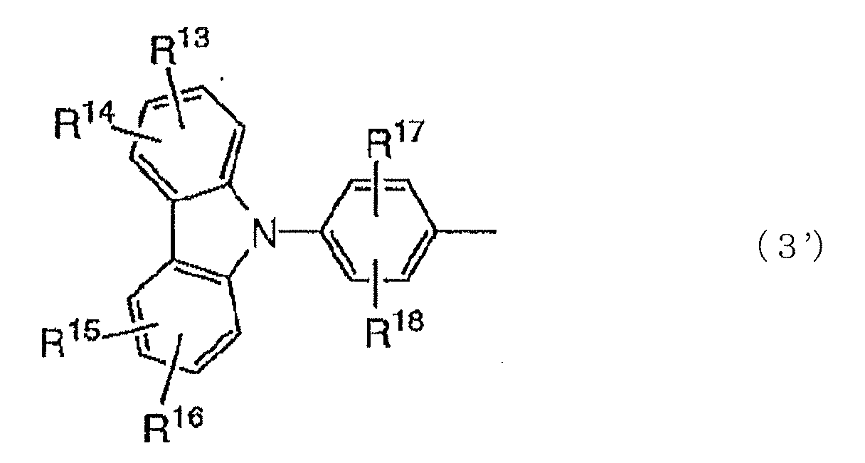
- Ar 8 represents a substituted or unsubstituted aryl group having 5 to 50 carbon atoms, a substituted or unsubstituted aromatic heterocyclic group having 3 to 40 carbon atoms, or a group expressed by the following general formula (3'): wherein R 13 to R 18 each independently represents a hydrogen atom, a halogen atom, a substituted or unsubstituted alkyl group having 1 to 20 carbon atoms, a substituted or unsubstituted aralkyl group having 6 to 30 carbon atoms, a substituted or unsubstituted alkenyl group having 3 to 30 carbon atoms, a cyano group, a substituted or unsubstituted amino group, an acyl group, a substituted or unsubstituted alkoxycarbonyl group having 2 to 30 carbon atoms, a carboxyl group, a substituted or unsubstituted alkoxy group having 1 to 30 carbon atoms, a substituted
- halogen atom examples include fluorine, chlorine, bromine and iodine.
- the substituted or unsubstituted amino group is represented by the formula: -NX 4 X 5 .
- the groups represented by X 4 and X 5 include a hydrogen atom, methyl, ethyl, propyl, isopropyl, n-butyl, s-butyl, isobutyl, t-butyl, n-pentyl, n-hexyl, n-heptyl, n-octyl, hydroxymethyl, 1-hydroxyethyl, 2-hydroxyethyl, 2-hydroxyisobutyl, 1,2-dihydroxyethyl, 1,3-dihydroxyisopropyl, 2,3-dihydroxy-t-butyl, 1,2,3-trihydroxypropyl, chloromethyl, 1-chloroethyl, 2-chloroethyl, 2-chloroisobutyl, 1,2-dichloroethyl, 1,3-dichloroisopropyl,
- substituted or unsubstituted alkyl group examples include methyl, ethyl, propyl, isopropyl, n-butyl, s-butyl, isobutyl, t-butyl, n-pentyl, n-hexyl, n-heptyl, n-octyl, hydroxymethyl, 1-hydroxyethyl, 2-hydroxyethyl, 2-hydroxyisobutyl, 1,2-dihydroxyethyl, 1,3-dihydroxyisopropyl, 2,3-dihydroxy-t-butyl, 1,2,3-trihydroxypropyl, chloromethyl, 1-chloroethyl, 2-chloroethyl, 2-chloroisobutyl, 1,2-dichloroethyl, 1,3-dichlorolsopropyl, 2,3-dichloro-t-butyl, 1,2,3-trichloropropyl, bromomethyl,
- substituted or unsubstituted alkenyl group examples include vinyl, allyl, 1-butenyl, 2-butenyl, 3-butenyl, 1,3-butanedienyl, 1-methylvinyl, styryl, 2,2-diphneylvinyl, 1,2-diphneylvinyl, 1-methylallyl, 1,1-dimethylallyl, 2-methylallyl, 1-phenylallyl, 2-phenylallyl, 3-phenylallyl, 3,3-diphneylallyl, 1,2-dimethylallyl, 1-phneyl-1-butenyl and 3-phneyl-1-butenyl.
- the substituted or unsubstituted alkoxy group is represented by the formula: -OY.
- the group Y include methyl, ethyl, propyl, isopropyl, n-butyl, s-butyl, isobutyl, t-butyl, n-pentyl, n-hexyl, n-heptyl, n-octyl, hydroxymethyl, 1-hydroxyethyl, 2-hydroxyethyl, 2-hydroxyisobutyl, 1,2-dihydroxyethyl, 1,3-dihydroxyisopropyl, 2,3-dihydroxy-t-butyl, 1,2,3-trihydroxypropyl, chloromethyl, 1-chloroethyl, 2-chloroethyl, 2-chloroisobutyl, 1,2-dichloroethyl, 1,3-dichloroisopropyl, 2,3-dichloro-t-butyl, 1,2,
- Examples of the substituted or unsubstituted aryl group include phenyl, 1-naphthyl, 2-naphthyl, 1-anthryl, 2-anthryl, 9-anthryl, 1-phenathryl, 2-phenathryl, 3-phenathryl, 4-phenathryl, 9-phenathryl, 1-naphthacenyl, 2-naphthacenyl, 9-naphthacenyl, 1-pyrenyl, 2-pyrenyl, 4-pyrenyl, 2-biphenylyl, 3-biphenylyl, 4-biphenylyl, p-terphenyl-4-yl, p-terphenyl-3-yl, p-terphenyl-2-yl, m-terphenyl-4-yl, m-terphenyl-3-yl, m-terphenyl-2-yl, o-tolyl, m-tolyl, p-toly
- Examples of the substituted or unsubstituted aromatic heterocyclic group include 1-pyrrolyl, 2-pyrrolyl, 3-pyrrolyl, pyrazinyl, 2-pyridinyl, 3-pyridinyl, 4-pyridinyl, 1-indolyl, 2-indolyl, 3-indolyl, 4-indolyl, 5-indolyl, 6-indolyl, 7-indolyl, 1-isoindolyl, 2-isoindolyl, 3-isoindolyl, 4-isoindolyl, 5-isoindolyl, 6-isoindolyl, 7-isoindolyl, 2-furyl, 3-furyl, 2-benzofuranyl, 3-benzofuranyl, 4-benzofuranyl, 5-benzofuranyl, 6-benzofuranyl, 7-benzofuranyl, 1-isobenzofuranyl, 3-isobenzofuranyl, 4-isobenzo
- Examples of the substituted or unsubstituted aralkyl group include benzyl, 1-phenylethyl, 2-phenylethyl, 1-phenylisopropyl, 2-phenylisopropyl, phenyl-t-butyl, ⁇ -naphthylmethyl, 1- ⁇ -naphthylethyl, 2- ⁇ -naphthylethyl, 1- ⁇ -naphthylisopropyl, 2- ⁇ -naphthylisopropyl, ⁇ -naphthylmethyl, 1- ⁇ -naphthylethyl, 2- ⁇ -naphthylethyl, 1- ⁇ -naphthylisopropyl, 2- ⁇ -naphthylisopropyl, 1-pyrrolylmethyl, 2-(1-pyrrolyl)ethyl, p-methylbenzyl, m-methylbenzyl, o
- the substituted or unsubstituted aryloxy group is represented by the formula: -OZ.
- the group Z include phenyl, 1-naphthyl, 2-naphthyl, 1-anthryl, 2-anthryl, 9-anthryl, 1-phenathryl, 2-phenathryl, 3-phenathryl, 4-phenathryl, 9-phenathryl, 1-naphthacenyl, 2-naphthacenyl, 9-naphthacenyl, 1-pyrenyl, 2-pyrenyl, 4-pyrenyl, 2-biphenylyl, 3-biphenylyl, 4-biphenylyl, p-terphenyl-4-yl, p-terphenyl-3-yl, p-terphenyl-2-yl, m-terphenyl-4-yl, m-terphenyl-3-yl, m-terphenyl-2-yl, o-to
- the substituted or unsubstituted alkoxycarbonyl group is represented by the formula: -COOY.
- the group Y include methyl, ethyl, propyl, isopropyl, n-butyl, s-butyl, isobutyl, t-butyl, n-pentyl, n-hexyl, n-heptyl, n-octyl, hydroxymethyl, 1-hydroxyethyl, 2-hydroxyethyl, 2-hydroxyisobutyl, 1,2-dihydroxyethyl, 1,3-dihydroxyisopropyl, 2,3-dihydroxy-t-butyl, 1,2,3-trihydroxypropyl, chloromethyl, 1-chloroethyl, 2-chloroethyl, 2-chloroisobutyl, 1,2-dichloroethyl, 1,3-dichloroisopropyl, 2,3-dichloro-t-buty
- Examples of the substituted or unsubstituted alkylamino group include amino groups which are substituted with the above exemplified alkyl groups.
- Examples of the substituted or unsubstituted aralkylamino group include amino groups which are substituted with the above exemplified aralkyl groups.
- Examples of the substituted or unsubstituted alkylene group include divalent groups derived from the above exemplified alkyl groups.
- Examples of the substituted or unsubstituted arylene group include divalent groups derived from the above exemplified aryl groups.
- divalent groups capable of forming a ring examples include tetramethylene, pentamethylene, hexamethylene, diphenylmethane-2,2'-di-yl, diphenylethane-3,3'-di-yl and diphenylpropane-4,4'-di-yl.
- substituent groups which may be bonded to the above respective groups include a hydrogen atom, a halogen atom, a hydroxyl group, an amino group, a nitro group, a cyano group, an alkyl group, an alkenyl group, a cycloalkyl group, an alkoxy group, an aryl group, an aromatic heterocyclic group, an aralkyl group, an aryloxy group, an alkoxycarbonyl group and a carboxyl group.
- substituent groups include the same groups as exemplified above.
- the host material contained in the light emitting layer thereof preferably has a triplet energy of 2.52 eV or higher since the resultant device is capable of emitting a red light.
- the triplet energy of the host material contained in the light emitting layer is more preferably 2.76 eV or higher and still more preferably 2.85 eV or higher since the device also has a high capability of emitting a blue light.
- the triplet energy of the host material contained in the light emitting layer is preferably 3.70 eV or lower because of facilitated injection of holes or electrons into the host material contained in the light emitting layer.
- the host material contained in the light emitting layer preferably exhibits an electron transporting property.
- the electron transporting property of the host material used herein means any of the following properties (1) and (2):
- the electron transporting property does not mean absence of a hole transporting property. Therefore, even if a material having an electron transporting property exhibits a hole mobility of 10 -7 cm 2 /Vs or higher upon the measurement, the material may be occasionally regarded as an electron transporting material.
- Polycarbazole compounds such as polyvinyl carbazole and biscarbazole conventionally used as the host material of the light emitting layer generally have a hole transporting property and exhibit a low electron transporting capability.
- the recombination zone is mainly formed near a cathode-side interface of the light emitting layer.
- the electron injecting layer when the electron injecting layer is interposed between the light emitting layer and the cathode, and an electron transporting material having a smaller energy gap than that of the host material in the light emitting layer is incorporated into the electron injecting layer, the excitation state caused around the cathode-side interface of the light emitting layer tends to be deactivated owing to the electron injecting layer, so that the efficiency of light emission is considerably lowered.
- the excitation state caused around the cathode-side interface of the light emitting layer also tends to be deactivated owing to the electron injecting layer, so that the efficiency of light emission is considerably lowered.
- the host material constituting the light emitting layer, or the light emitting layer itself exhibits an electron transporting property
- the zone of recombination of electrons and holes is separated apart from the interface between the electron injecting layer and the light emitting layer, so that deactivation of the excitation state is effectively prevented.
- the host material constituting the light emitting layer is preferably made of an electron-deficient derivative of five-membered ring having nitrogen or an electron-deficient derivative of six-membered ring.
- the "electron deficiency" used herein means that one or more of carbon atoms of a 6 ⁇ aromatic ring are replaced with nitrogen atoms.
- the derivative of five-membered ring having nitrogen preferably has at least one skeleton selected from the group consisting of imidazole, benzimidazole, triazole, tetrazole, oxadiazole, thiadiazole, oxatriazole and thiatriazole, and more preferably has a skeleton of imidazole or benzimidazole.
- the derivative of six-membered ring having nitrogen preferably has at least one skeleton selected from the group consisting of triazine, quinoxaline, quinoline, benzopyrimidine, pyridine, pyrazine and pyrimidine, and more preferably has a skeleton of triazine or pyrimidine.
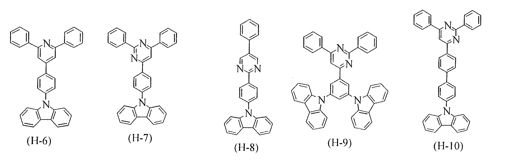
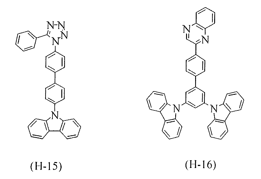
- the host material contained in the light emitting layer is preferably a compound represented by the following general formula (5) or (6).
- (Cz ⁇ ) m A wherein Cz represents a substituted or unsubstituted carbazolyl group or a substituted or unsubstituted azacarbazolyl group; A represents an aryl-substituted ring group having nitrogen, a diaryl-substituted ring group having nitrogen or a triaryl-substituted ring group having nitrogen; and m is an integer of 1 to 3.
- examples of the preferred ring having nitrogen include pyridine, quinoline, pyrazine, pyrimidine, quinoxaline, triazine, imidazole and imidazopyridine.
- the ionization potential thereof is determined by the position of Cz, and is in the range of 5.6 to 5.8 eV.
- the phosphorescent light emitting materials to be contained in the light emitting layer are preferably organic metal complexes in view of enhancing an external quantum efficiency of the device.
- organic metal complexes more preferred are palladium complexes, iridium complexes, osmium complexes and platinum complexes; still more preferred are iridium complexes and platinum complexes; and most preferred are ortho-metallized iridium complexes.
- the organic EL device of the present invention is preferably provided with an electron injecting layer.
- An electron transporting material contained in the electron injecting layer is preferably made of nitrogen-containing complexes in the form of a metal complex containing a single kind of nitrogen-containing ring derivative as a ligand.
- nitrogen-containing ring examples include quinoline, phenyl pyridine, benzoquinone and phenathroline.
- the preferred metal complexes include quinolinol metal complexes and derivatives thereof.
- quinolinol metal complexes and derivatives thereof include metal complexes containing a 8-quinolinol derivative as a ligand, for example, tris(8-quinolinol)Al complexes, tris(5,7-dichloro-8-quinolinol)Al complexes, tris(5,7-dibromo-8-quinolinol)Al complexes, tris(2-methyl-8-quinolinol)Al complexes, tris(5-methyl-8-quinolinol)Al complexes, tris(8-quinolinol)Zn complexes, tris(8-quinolinol)In complexes, tris(8-quinolinol)Mg complexes, tris(8-quinolinol)Cu complexes, tris(8-quinolinol)Ca complexes, tris(8-quinolinol)Sn complexes, tris(8-quinolino
- These metal complexes are excellent in injection of electrons from the cathode because of a small energy gap thereof, as well as exhibit a high durability to electron transportation, thereby providing devices having a long lifetime.
- the organic EL device of the present invention is preferably provided, at an interface between the light emitting layer and the hole transporting layer, with a zone where electrons and holes are recombined with each other, or a light emitting zone.
- the recombination or light emission in such zones means that when a phosphorescent light emitting material is added to the interfacial zone, the efficiency of light emission is enhanced as compared to the case where the phosphorescent light emitting material is added to zones other than the interfacial zone.
- Examples of the construction of the organic EL device according to the present invention include layer structures such as an anode/a hole transporting layer/a light emitting layer/a cathode; an anode/a hole transporting layer/a light emitting layer/an electron injecting layer/a cathode; an anode/a hole injecting layer/a hole transporting layer/a light emitting layer/an electron injecting layer/a cathode; and an anode/an insulting layer/a hole injecting layer/a hole transporting layer/a light emitting layer/an electron injecting layer/a cathode.
- an inorganic compound layer or an electron transporting layer which is made of an insulating material or a semiconductor may be disposed between the electron injecting layer and the cathode. These layers are capable of effectively preventing leakage of current and enhancing an electron injecting property.
- the insulating material there is preferably used at least one metal compound selected from the group consisting of alkali metal chalcogenides, alkali earth metal chalcogenides, alkali metal halides and alkali earth metal halides.
- the electron transporting layer made of these alkali metal chalcogenides, etc., is preferred since the electron injecting property thereof can be further enhanced.
- Specific examples of the preferred alkali metal chalcogenides include Li 2 O, LiO, Na 2 S, Na 2 Se and NaO.
- Specific examples of the preferred alkali earth metal chalcogenides include CaO, BaO, SrO, BeO, BaS and CaSe.
- preferred alkali metal halides include LiF, NaF, KF, LiCl, KCl and NaCl.
- preferred alkali earth metal halides include fluorides such as CaF 2 , BaF 2 , SrF 2 , MgF 2 and BeF 2 , and halides other than these fluorides.
- the semiconductor include oxides, nitrides and oxinitrides containing at least one element selected from the group consisting of Ba, Ca, Sr, Yb, Al, Ga, In, Li, Na, Cd, Mg, Si, Ta, Sb and Zn. These semiconductors may be used singly or in combination of any two or more thereof.
- the inorganic compound constituting the electron transporting layer is preferably in the form of a microcrystalline or amorphous insulating thin film.
- the electron transporting layer made of such an insulating thin film can be prevented from suffering from pixel deficiency such as dark spots owing to formation of a more uniform thin film.
- the inorganic compound include the above-mentioned alkali metal chalcogenides, alkali earth metal chalcogenides, alkali metal halides and alkali earth metal halides.
- a layer which comes into contact with the cathode preferably contains a reductive dopant.
- the reductive dopant preferably has a work function of 2.9 eV or lower.
- the reductive dopant is defined as a compound capable of enhancing an electron injection efficiency, and enables at least a part of the electron injecting layer into which the reductive dopant is added, or the interfacial zone thereof, to be reduced and converted into anions.
- the reductive dopant added to the interfacial zone is preferably in the form of a layer or an island.
- the reductive dopant there is preferably used at least one substance selected from the group consisting of alkali metals, alkali metal complexes, alkali metal compounds, alkali earth metals, alkali earth metal complexes, alkali earth metal compounds, rare earth metals, rare earth metal complexes and rare earth metal compounds.
- the alkali metal compounds, alkali earth metal compounds and rare earth metal compounds may be in the form of an oxide or a halide.
- alkali metals examples include Na (work function: 2.36 eV), K (work function: 2.28 eV), Rb (work function: 2.16 eV) and Cs (work function: 1.95 eV).
- the alkali metals are preferably those having a work function of 2.9 eV or lower. Of these alkali metals, preferred are K, Rb and Cs, more preferred are Rb and Cs, and most preferred is Cs.
- alkali earth metals examples include Ca (work function: 2.9 eV), Sr (work function: 2.0 to 2.5 eV) and Ba (work function: 2.52 eV).
- the alkali earth metals are preferably those having a work function of 2.9 eV or lower.
- rare earth metals examples include Sc, Y, Ce, Tb and Yb.
- the rare earth metals are preferably those having a work function of 2.9 eV or lower.
- the above preferred metals can exhibit a high reducing capability and are capable of enhancing a luminance of light emitted from the organic EL device, and prolonging a lifetime thereof even when they are added to the electron injecting zone in a relatively small amount.
- alkali metal compounds examples include alkali metal oxides such as Li 2 O, Cs 2 O and K 2 O, and alkali metal halides such as LiF, NaF, CsF and KF. Of these alkali metal compounds, preferred are alkali metal oxides and alkali metal fluorides such as LiF, Li 2 O and NaF.
- alkali earth metal compounds examples include BaO, SrO, CaO and mixtures thereof such as Ba x Sr 1-x O (0 ⁇ x ⁇ 1) and Ba x Ca 1-x O (0 ⁇ x ⁇ 1). Of these alkali earth metal compounds, preferred are BaO, SrO and CaO.
- rare earth metal compounds examples include YbF 3 , ScF 3 , ScO 3 , Y 2 O 3 , Ce 2 O 3 , GdF 3 and TbF 3 . Of these rare earth metal compounds, preferred are YbF 3 , ScF 3 and TbF 3 .
- alkali metal complexes, alkali earth metal complexes and rare earth metal complexes are not particularly limited as long as these complexes respectively contain at least one metal ion selected from alkali metal ions, alkali earth metal ions and rare earth metal ions.
- Examples of the preferred ligand contained in these complexes include quinolinol, benzoquinolinol, acridinol, phenanthridinol, hydroxyphenyl oxazole, hydroxyphenyl thiazole, hydroxydiaryl oxadiazole, hydroxydiaryl thiadiazole, hydroxyphenyl pyridine, hydroxydiaryl benzoimidazole, hydroxybenzotriazole, hydroxyflavone, bipyridyl, phenanthroline, phthalocyanine, porphyrin, cyclopentadiene, ⁇ -diketones, azomethines and derivatives thereof, though not particularly limited thereto.
- the layer containing the reductive dopant is preferably produced by the following method. That is, while vapor-depositing the reductive dopant by resistance heating vapor deposition method, an organic substance as the light emitting material or electron injecting material constituting the interfacial zone is vapor-deposited simultaneously, thereby dispersing the reductive dopant in the organic substance.
- the concentration of dispersion of the layer is controlled such that the molar ratio of the organic substance to the reductive dopant is 100:1 to 1:100 and preferably 5:1 to 1:5.
- the reductive dopant is singly vapor-deposited thereon by resistance heating vapor deposition method to form a layer having a thickness of preferably 0.1 to 15 nm.
- the reductive dopant is singly vapor-deposited thereon by resistance heating vapor deposition method to form islands each having a thickness of preferably 0.05 to 1 nm.
- the hole transporting layer in the organic EL device of the present invention is the same as described above.
- the organic EL device of the present invention further include a hole injecting layer.
- the hole injecting layer is preferably made of a material capable of transporting holes into the light emitting layer under a still lower field intensity.
- the hole mobility of the hole injecting material is preferably at least 10 -4 cm 2 /V ⁇ second, for example, upon applying an electric field of 10 4 to 10 6 V/cm.
- the hole injecting material may be optionally selected from conventionally known materials which are ordinarily used as charge transfer materials for holes in photoconductive materials or ordinarily used in the hole injecting layer of organic EL devices.
- the hole injecting material is preferably made of a compound which has a hole transporting capability as well as an excellent effect of injecting holes from the anode and further into the light emitting layer or the light emitting material or prevents excitons produced in the light emitting layer from transferring to the electron injecting layer or the electron injecting material, and exhibits an excellent thin film-forming capability.
- Such a compound include phthalocyanine derivatives, naphthalocyanine derivatives, porphyrin derivatives, oxazole, oxadiazole, triazole, imidazole, imidazolone, imidazole thione, pyrazoline, pyrazolone, tetrahydroimidazole, hydrazone, acylhydrazone, polyarylalkane, stilbene, butadiene, benzidine-type triphenylamine, styrylamine-type triphenylamine, diamine-type triphenylamine and derivatives thereof, as well as polymer materials such as polyvinyl carbazole, polysilane and conductive polymers, though not particularly limited thereto.
- more effective hole injecting materials are aromatic tertiary amine derivatives or phthalocyanine derivatives.
- aromatic tertiary amine derivatives include triphenylamine, tritolylamine, tolyldiphenylamine, N,N'-diphenyl-N,N'-(3-methylphenyl)-1,1'-biphenyl-4,4'-diamine, N,N,N',N'-(4-methylphenyl)-1,1'-pheliyl-4,4'-diamine, N,N,N',N'(4-methylphenyl)-1,1'-biphenyl-4,4'-diamine, N,N'-diphenyl-N,N'-dinaphthyl-1,1'-biphenyl-4,4'-diamine, N,N'-(methylphenyl)-N,N'-(4-n-butylphenyl)-phen
- phthalocyanine (Pc) derivatives include phthalocyanine derivatives and naphthalocyanine derivatives such as H 2 Pc, CuPc, CoPc, NiPc, ZnPc, PdPc, FePc, MnPc, ClAlPc, ClGaPc, ClInPc, ClSnPc, Cl 2 SiPc, (HO)AlPc, (HO)GaPc, VOPc, TiOPc, MoOPc and GaPc-O-GaPc, though not particularly limited thereto.
- phthalocyanine (Pc) derivatives include phthalocyanine derivatives and naphthalocyanine derivatives such as H 2 Pc, CuPc, CoPc, NiPc, ZnPc, PdPc, FePc, MnPc, ClAlPc, ClGaPc, ClInPc, ClSnPc, Cl 2 SiPc, (HO)AlPc, (HO)GaP
- the anode of the organic EL device has a function of injecting holes into the hole transporting layer or the light emitting layer, and effectively exhibits a work function of 4.5 eV or higher.
- the anode material usable in the present invention indium tin oxide (ITO) alloys, tin oxide (NESA), gold, silver, platinum and copper.
- the cathode is preferably made of a material having a small work function in order to inject electrons into the electron transporting layer or the light-emitting layer.
- cathode material examples include, but not particularly limited to, indium, aluminum, magnesium, magnesium-indium alloys, magnesium-aluminum alloys, aluminum-lithium alloys, aluminum-scandium-lithium alloys and magnesium-silver alloys.
- the respective layers of the organic EL device of the present invention may be formed by conventionally known methods such as vacuum vapor deposition method and spin-coating method without any particular limitation.
- the organic thin film layers used in the organic EL device of the present invention may be produced by known methods such as vacuum vapor deposition method, molecular beam epitaxy (MBE) method, dipping method using a solution prepared by dissolving the respective materials in a solvent, as well as coating methods such as spin-coating method, cast-coating method, bar-coating method and roller-coating method.
- the thickness of the respective organic thin film layers in the organic EL device of the present invention is not particularly limited, and is usually in the range of from several nm to 1 ⁇ m, since a too small film thickness thereof tends to cause defects such as pin holes, whereas a too large film thickness thereof tends to cause a poor efficiency owing to need of applying a high voltage thereto.
- the hole mobility was measured by a time-of-flight (TOF) method. That is, a hole transporting material as a sample was applied onto an ITO substrate to form thereon a coating film having thickness of 2.5 ⁇ m, and a counter electrode made of Al was disposed in an opposed relation thereto. Then, a voltage was applied between both the electrodes at a field intensity of 0.1 to 0.6 MV/cm, and further a N 2 laser (pulse width: 2 ns) was irradiated thereto to measure the resultant electric current using a storage oscilloscope (measuring frequency band: 300 MHz).
- TOF time-of-flight
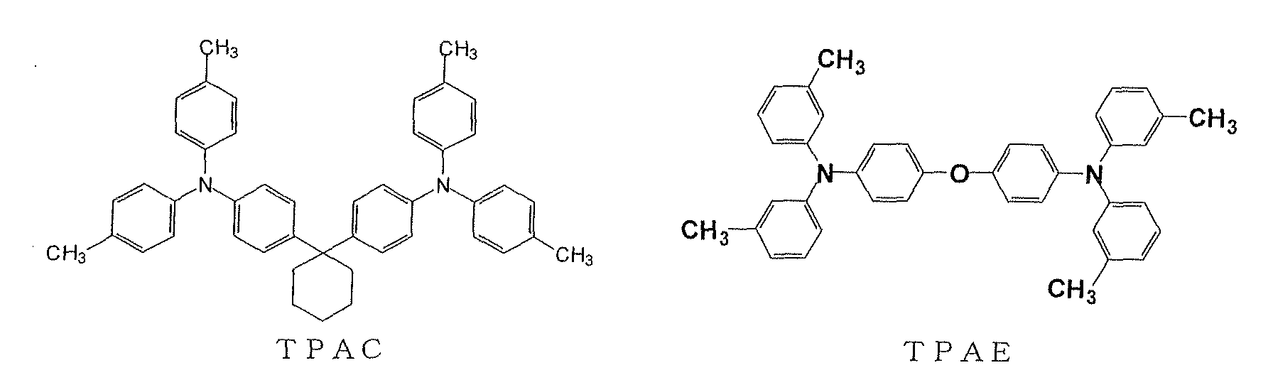
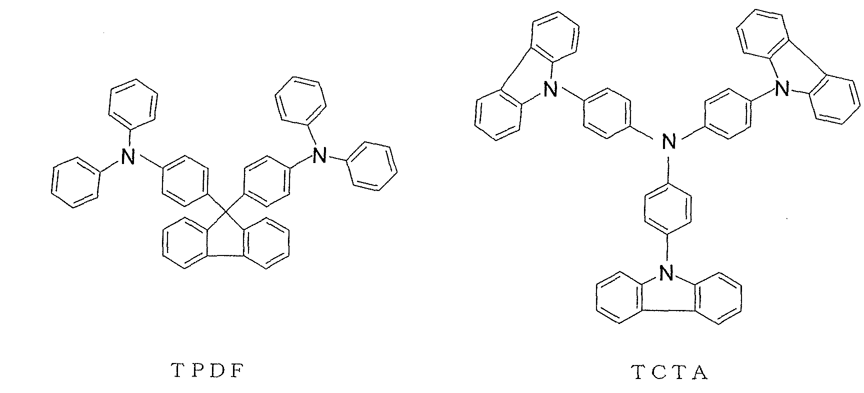
- the ionization potential of particles of the respective materials was measured using an atmospheric photoelectron spectrometer "AC-1" available from Riken Keiki Co., Ltd. Measurement Examples Kind of compound Light emitting end (nm) Triplet energy (eV) 1 NPD 504 2.46 2 TPD 494 2.51 3 TPAC 413 3.00 4 TPAE 411 3.02 5 TPDF 413 3.00 6 DCTA 420 2.95 7 TCTA 420 2.95 8 BCBCz 432 2.82 Measurement Examples Field intensity (MV/cm 2 ) Hole mobility (cm 2 /Vs) Ionization potential (eV) 1 0.2 0.8 x 10 -3 5.4 2 0.2 0.9 x 10 -3 5.4 3 0.2 1.2 x 10 -3 5.6 4 0.3 0.2 x 10 -3 5.5 5 0.3 0.8 x 10 -3 5.7 6 0.25 0.7 x 10 -3 5.4 7 0.25 0.8 x 10 -3 5.4 8 0.3 0.3 x 10 -3 5.6
- the thus cleaned glass substrate with the transparent electrode was attached to a substrate holder of a vacuum deposition apparatus.
- a 10 nm-thick film made of copper phthalocyanine hereinafter referred to merely as "CuPc film” was formed on a surface of the substrate on which the transparent electrode was provided, so as to cover the transparent electrode.
- CuPc film 10 nm-thick film made of copper phthalocyanine
- a 30 nm-thick film made of the above TPAC as the hole transporting material was formed on the CuPc film.
- the thus formed TPAC film functioned as a hole transporting layer.
- the below-mentioned compound PB102 as a host material was vapor-deposited on the TPAC film to form a 30 nm-thick light emitting layer thereon.
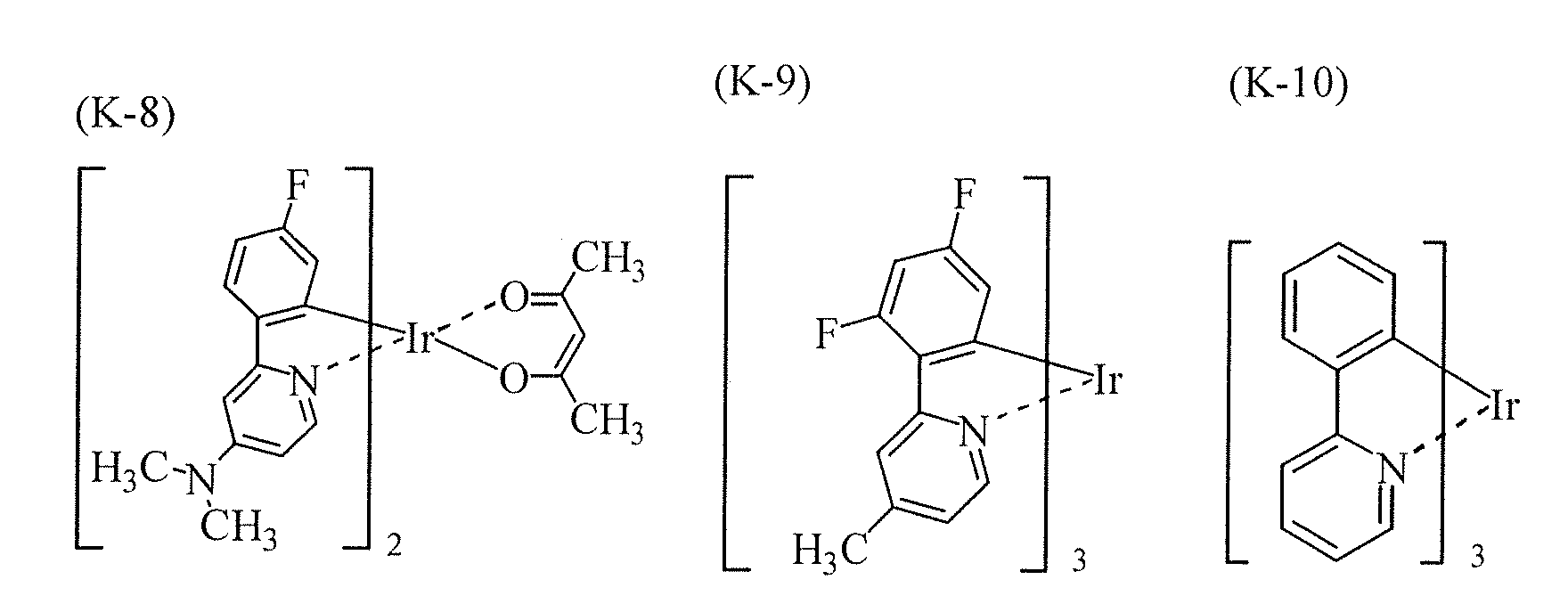
- the above compound (K-3) as a phosphorescent Ir metal complex was added thereto.
- the content of the compound (K-3) in the light emitting layer was 7% by weight.
- the resultant layer functioned as a light emitting layer.
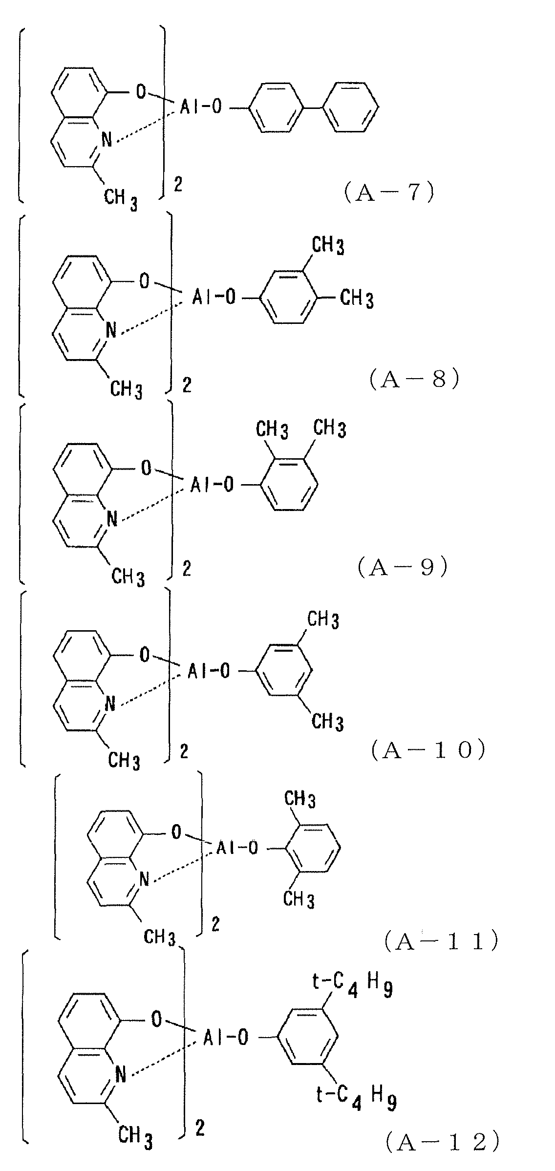
- A-7 film made of (1,1'-bisphenyl)-4-olato) bis(2-methyl-8-quinolinolato) aluminum (film made of the above compound (A-7)) was formed on the light emitting layer.
- the thus formed A-7 film functioned as an electron injecting layer.
- Li as a reductive dopant lithium source available from SAES Getter S.p.A.
- the compound (A-7) were subjected to binary vapor deposition to form a (A-7):Li film as a cathode-side electron injecting layer.
- a metallic Al was vapor-deposited on the (A-7):Li film to form a metal cathode, thereby producing an organic EL device.
- the excitation energy of the Ir metal complex K ⁇ 10 as the host material of the light emitting layer was 2.55 eV, and the obtained device was free from deactivation of the excitation state and exhibited an extremely high current efficiency. Meanwhile, the excitation energy of the Ir metal complex was measured by the same method as used for measurement of the triplet energy.
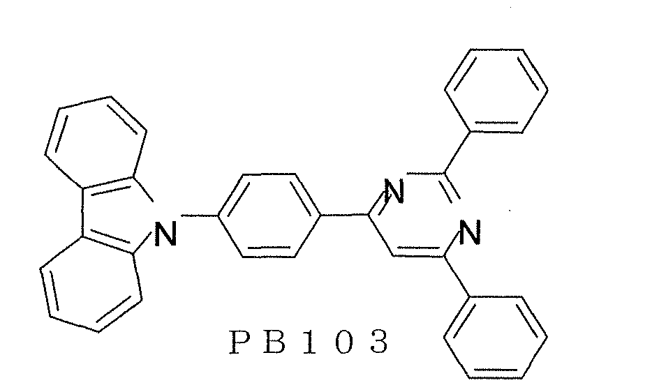
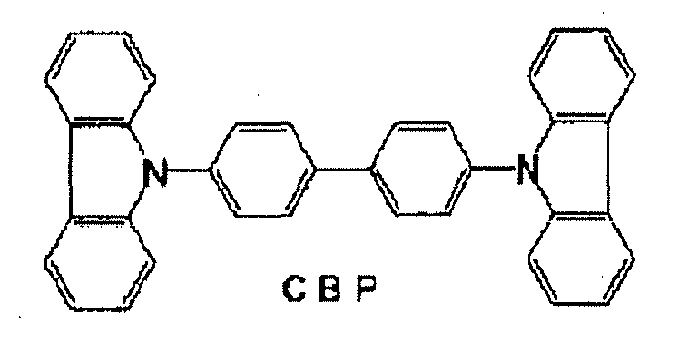
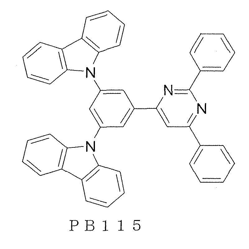
- Example 10 As shown in Table 4, from the comparison between the results of Example 10 and the results of Examples 8 and 9, it was confirmed that when the material containing pyridine or pyridinoimidazole as an electron-deficient ring was used as the host material of the light emitting layer, the obtained device exhibited a very high current efficiency. This was because the host materials used in Examples 8 and 9 were an electron transporting material, so that electrons and holes were recombined with each other at an interface between the host material and the hole transporting layer, and the excitation state generated in the host material was free from deactivation due to the hole transporting material.
- the thus cleaned glass substrate with the transparent electrode was attached to a substrate holder of a vacuum deposition apparatus.
- a 10 nm-thick CuPc film was formed on a surface of the substrate on which the transparent electrode was provided, so as to cover the transparent electrode.
- the thus formed CuPc film functioned as a hole injecting layer.
- the substrate was attached again to the substrate holder of the vacuum deposition apparatus, and then the above compound PB102 was vapor-deposited on the hole transporting layer to form a 30 nm-thick light emitting layer thereon.
- the above compound (K-3) as a phosphorescent Ir metal complex was added thereto.
- the content of the compound (K-3) in the light emitting layer was 7% by weight.
- the resultant film functioned as a light emitting layer.
- a 10 nm-thick film made of the above compound (A-7) was formed on the light emitting layer.
- the thus formed A-7 film functioned as an electron injecting layer.
- Li as a reductive dopant lithium source available from SAES Getter S.p.A.
- the compound (A-7) were subjected to binary vapor deposition to form a (A-7):Li film as a cathode-side electron injecting layer.
- a metallic Al was vapor-deposited on the (A-7):Li film to form a metal cathode, thereby producing an organic EL device.
- the organic EL device using as the material of the hole transporting layer polyvinyl carbazole whose hole mobility was as low as 2 x 10 -7 cm 2 /Vs, required application of a considerably high driving voltage. Further, in addition to the above high driving voltage, the obtained organic EL device was also deteriorated in current efficiency as compared to those obtained in Examples. Accordingly, it was recognized that when the hole mobility became low, especially the current efficiency was largely affected by the low hole mobility.
- the hole transporting material constituting the hole transporting layer has a triplet energy of 2.52 to 3.70 eV and a hole mobility of 10 -6 cm 2 /Vs or higher as measured at a field intensity of 0.1 to 0.6 MV/cm. Therefore, the organic electroluminescence device can emit a phosphorescent light at a favorable current efficiency and has a long lifetime and, therefore, is useful as an organic electroluminescence device for full color display.
Landscapes
- Chemical & Material Sciences (AREA)
- Physics & Mathematics (AREA)
- Engineering & Computer Science (AREA)
- Materials Engineering (AREA)
- Optics & Photonics (AREA)
- Spectroscopy & Molecular Physics (AREA)
- Organic Chemistry (AREA)
- Inorganic Chemistry (AREA)
- Electroluminescent Light Sources (AREA)
Abstract
Description

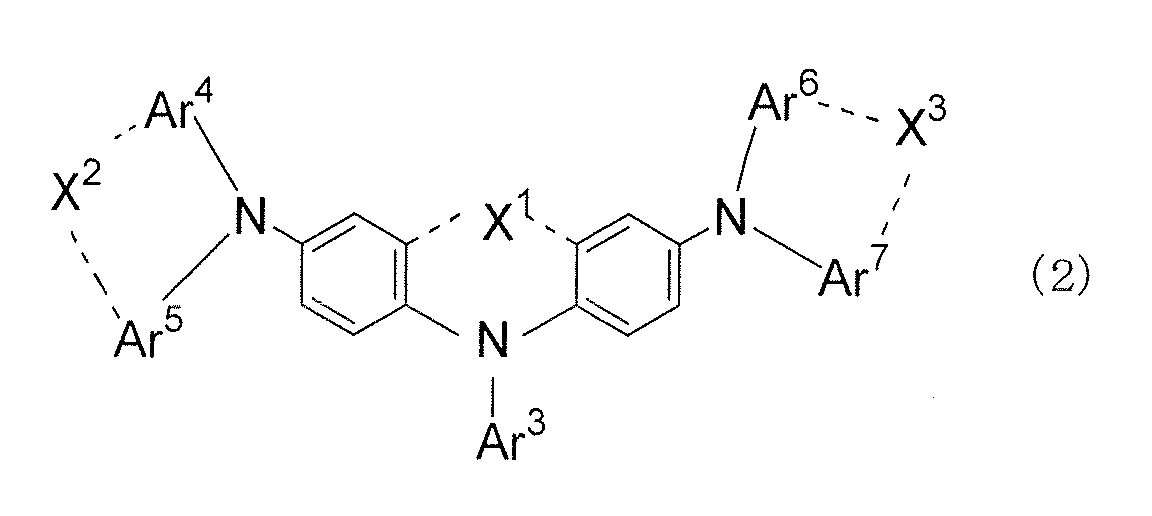

X represents a trivalent coupling group expressed by any of the following formulae:


Compounds represented by the following general formula (4):








Specific examples of the aromatic tertiary amine derivatives include triphenylamine, tritolylamine, tolyldiphenylamine,
N,N'-diphenyl-N,N'-(3-methylphenyl)-1,1'-biphenyl-4,4'-diamine,
N,N,N',N'-(4-methylphenyl)-1,1'-pheliyl-4,4'-diamine,
N,N,N',N'(4-methylphenyl)-1,1'-biphenyl-4,4'-diamine,
N,N'-diphenyl-N,N'-dinaphthyl-1,1'-biphenyl-4,4'-diamine,
N,N'-(methylphenyl)-N,N'-(4-n-butylphenyl)-phenanthrene-9,10-diamine and
N,N-bis(4-di-4-tolylaminophenyl)-4-phenyl-cyclohexane, as well as oligomers or polymers having these aromatic tertiary amine skeletons, though not particularly limited thereto. Specific examples of the phthalocyanine (Pc) derivatives include phthalocyanine derivatives and naphthalocyanine derivatives such as H2Pc, CuPc, CoPc, NiPc, ZnPc, PdPc, FePc, MnPc, ClAlPc, ClGaPc, ClInPc, ClSnPc, Cl2SiPc, (HO)AlPc, (HO)GaPc, VOPc, TiOPc, MoOPc and GaPc-O-GaPc, though not particularly limited thereto.


| Measurement Examples | Kind of compound | Light emitting end (nm) | Triplet energy (eV) |
| 1 | NPD | 504 | 2.46 |
| 2 | TPD | 494 | 2.51 |
| 3 | TPAC | 413 | 3.00 |
| 4 | TPAE | 411 | 3.02 |
| 5 | TPDF | 413 | 3.00 |
| 6 | DCTA | 420 | 2.95 |
| 7 | TCTA | 420 | 2.95 |
| 8 | BCBCz | 432 | 2.82 |
| Measurement Examples | Field intensity (MV/cm2) | Hole mobility (cm2/Vs) | Ionization potential (eV) |
| 1 | 0.2 | 0.8 x 10⁻³ | 5.4 |
| 2 | 0.2 | 0.9 x 10⁻³ | 5.4 |
| 3 | 0.2 | 1.2 x 10⁻³ | 5.6 |
| 4 | 0.3 | 0.2 x 10⁻³ | 5.5 |
| 5 | 0.3 | 0.8 x 10⁻³ | 5.7 |
| 6 | 0.25 | 0.7 x 10⁻³ | 5.4 |
| 7 | 0.25 | 0.8 x 10⁻³ | 5.4 |
| 8 | 0.3 | 0.3 x 10⁻³ | 5.6 |

| Hole transporting material | |||
| Kind | Triplet energy (eV) | Hole mobility (cm2/Vs) | |
| Example 1 | TPAC | 3.00 | 1.2 x 10⁻³ |
| Example 2 | TPDF | 3.00 | 0.8 x 10⁻³ |
| Example 3 | DCTA | 2.95 | 0.7 x 10⁻³ |
| Example 4 | TCTA | 2.73 | 0.8 x 10⁻³ |
| Example 5 | BCBCz | 2.82 | 0.3 x 10⁻³ |
| Comparative Example 1 | NPD | 2.46 | 0.8 x 10⁻³ |
| Comparative Example 2 | TPD | 2.51 | 0.9 x 10⁻³ |
| Evaluation of characteristics of organic EL device | ||||
| Voltage (V) | Luminance (cd/m2) | Current efficiency (cd/A) | Color of light emitted | |
| Example 1 | 8.4 | 93 | 12.3 | Bluish green |
| Example 2 | 9.5 | 85 | 12.1 | Bluish green |
| Example 3 | 9.2 | 110 | 13.2 | Bluish green |
| Example 4 | 9.0 | 112 | 12.9 | Bluish green |
| Example 5 | 9.1 | 85 | 11.5 | Bluish green |
| Comparative Example 1 | 11.5 | 82 | 0.75 | Blue |
| Comparative Example 2 | 11.8 | 78 | 1.23 | Blue |
| Hole transporting material | |||
| Kind | Triplet energy (eV) | Hole mobility (cm2/Vs) | |
| Example 6 | TPAC | 3.00 | 1.2 x 10⁻³ |
| Example 7 | TPDF | 3.00 | 0.8 x 10⁻³ |
| Comparative Example 3 | NPD | 2.46 | 0.8 x 10⁻³ |
| Comparative Example 4 | TPD | 2.51 | 0.9 x 10⁻³ |
| Evaluation of characteristics of organic EL device | ||||
| Voltage (V) | Luminance (cd/m2) | Current efficiency (cd/A) | Color of light emitted | |
| Example 6 | 5.8 | 150 | 38.5 | Green |
| Example 7 | 5.7 | 142 | 35.0 | Green |
| Comparative Example 3 | 5.4 | 100 | 22.5 | Green |
| Comparative Example 4 | 5.7 | 106 | 23.5 | Green |
| Hole transporting material | Light emitting layer | ||||
| Kind | Triplet energy (eV) | Hole mobility (cm2/Vs) | Kind of host material | Triplet energy (eV) | |
| Example 8 | TPAC | 3.00 | 1.2 x 10⁻³ | PB103 | 2.82 |
| Example 9 | TPAC | 3.00 | 1.2 x 10⁻³ | PB115 | 2.90 |
| Example 10 | TPAC | 3.00 | 1.2 x 10⁻³ | CBP | 2.81 |
| Comparative Example 5 | NPD | 2.46 | 0.8 x 10⁻³ | CBP | 2.81 |
| Evaluation of characteristics of organic EL device | ||||
| Voltage (V) | Luminance (cd/m2) | Current efficiency (cd/A) | Color of light emitted | |
| Example 8 | 5.8 | 150 | 39.5 | Green |
| Example 9 | 5.7 | 142 | 36.0 | Green |
| Example 10 | 5.1 | 102 | 22.6 | Green |
| Comparative Example 5 | 4.9 | 98 | 15.0 | Green |
Claims (10)
- An organic electroluminescence device, comprising a cathode, an anode and sandwiched between the cathode and the anode, at least a hole transporting layer and a light emitting layer containing a phosphorescent light emitting material and a host material, wherein the hole transporting layer comprises a hole transporting material having a triplet energy of 2.52 to 3.70 eV and a hole mobility of 10-6 cm2/Vs or higher as measured at a field intensity of 0.1 to 0.6 MV/cm.
- The organic electroluminescence device according to claim 1, wherein the hole transporting material has an ionization potential of 5.8 eV or lower.
- The organic electroluminescence device according to claim 1, wherein the hole transporting material has a triplet energy of 2.76 to 3.70 eV.
- The organic electroluminescence device according to claim 1, wherein the host material contained in the light emitting layer has a triplet energy of 2.52 eV or higher.
- The organic electroluminescence device according to claim 1, wherein the host material contained in the light emitting layer has an electron transporting property.
- The organic electroluminescence device according to claim 1, wherein the host material contained in the light emitting layer is made of an electron-deficient derivative of five-membered ring having nitrogen or of an electron-deficient derivative of six-membered ring having nitrogen.
- The organic electroluminescence device according to claim 6, wherein the derivative of five-membered ring having nitrogen has at least one skeleton selected from the group consisting of imidazole, triazole, tetrazole, oxadiazole, thiadiazole, oxatriazole and thiatriazole.
- The organic electroluminescence device according to claim 6, wherein the derivative of six-membered ring having nitrogen has at least one skeleton selected from the group consisting of quinoxaline, quinoline, benzopyrimidine, pyridine, pyrazine and pyrimidine.
- The organic electroluminescence device according to claim 1, wherein a zone where electrons and holes recombine with each other or a light emitting zone is provided at an interface between the light emitting layer and the hole transporting layer.
- The organic electroluminescence device according to claim 1, wherein a layer adjacent to the cathode contains a reductive dopant.
Applications Claiming Priority (3)
| Application Number | Priority Date | Filing Date | Title |
|---|---|---|---|
| JP2003016505 | 2003-01-24 | ||
| JP2003016505 | 2003-01-24 | ||
| PCT/JP2004/000236 WO2004066685A1 (en) | 2003-01-24 | 2004-01-15 | Organic electroluminescence device |
Publications (3)
| Publication Number | Publication Date |
|---|---|
| EP1589789A1 true EP1589789A1 (en) | 2005-10-26 |
| EP1589789A4 EP1589789A4 (en) | 2008-03-05 |
| EP1589789B1 EP1589789B1 (en) | 2015-07-01 |
Family
ID=32767480
Family Applications (1)
| Application Number | Title | Priority Date | Filing Date |
|---|---|---|---|
| EP04702427.8A Expired - Lifetime EP1589789B1 (en) | 2003-01-24 | 2004-01-15 | Organic electroluminescence device |
Country Status (7)
| Country | Link |
|---|---|
| US (2) | US20060180806A1 (en) |
| EP (1) | EP1589789B1 (en) |
| JP (1) | JP4580342B2 (en) |
| KR (1) | KR101035818B1 (en) |
| CN (1) | CN100493286C (en) |
| TW (1) | TW200417279A (en) |
| WO (1) | WO2004066685A1 (en) |
Cited By (15)
| Publication number | Priority date | Publication date | Assignee | Title |
|---|---|---|---|---|
| WO2007088377A1 (en) * | 2006-02-03 | 2007-08-09 | Cdt Oxford Limited | Phosphorescent organic light emissive device |
| EP1946392A2 (en) * | 2005-11-07 | 2008-07-23 | Oled-T Limited | Electroluminescent devices |
| WO2009099705A1 (en) * | 2008-02-09 | 2009-08-13 | Universal Display Corporation | Organic licht emitting device with a non-emissive organometallic layer |
| EP1956008A4 (en) * | 2005-11-30 | 2010-12-01 | Mitsubishi Chem Corp | ORGANIC COMPOUND, CHARGE TRANSPORT MATERIAL, COMPOSITION FOR CHARGE TRANSPORT MATERIAL, AND ELECTROLUMINESCENT ORGANIC DEVICE |
| US8288187B2 (en) | 2010-01-20 | 2012-10-16 | Universal Display Corporation | Electroluminescent devices for lighting applications |
| WO2013022419A1 (en) * | 2011-08-05 | 2013-02-14 | Universal Display Corporation | Phosphorescent organic light emitting devices combined with hole transport material having high operating stability |
| EP2568030A2 (en) | 2010-05-03 | 2013-03-13 | Cheil Industries Inc. | Compound for organic optoelectronic device, organic light emitting diode including same, and display device including organic light emitting diode |
| EP2616462A1 (en) | 2010-09-17 | 2013-07-24 | Rohm And Haas Electronic Materials Korea Ltd. | Novel organic electroluminescent compounds and organic electroluminescent device using the same |
| US8513658B2 (en) | 2008-09-04 | 2013-08-20 | Universal Display Corporation | White phosphorescent organic light emitting devices |
| US8866377B2 (en) | 2006-12-28 | 2014-10-21 | Universal Display Corporation | Long lifetime phosphorescent organic light emitting device (OLED) structures |
| US9306175B2 (en) | 2009-10-23 | 2016-04-05 | Hodogaya Chemical Co., Ltd. | Organic electroluminescent device |
| EP2492985A4 (en) * | 2009-10-23 | 2017-03-29 | Hodogaya Chemical Co., Ltd. | Organic electroluminescent element |
| CN110088926A (en) * | 2016-11-16 | 2019-08-02 | 保土谷化学工业株式会社 | Organic electroluminescent device |
| US10403839B2 (en) | 2011-02-16 | 2019-09-03 | Semiconductor Energy Laboratory Co., Ltd. | Light-emitting element |
| US10439156B2 (en) | 2013-05-17 | 2019-10-08 | Semiconductor Energy Laboratory Co., Ltd. | Light-emitting element, light-emitting device, display device, lighting device, and electronic device |
Families Citing this family (42)
| Publication number | Priority date | Publication date | Assignee | Title |
|---|---|---|---|---|
| JP2004311410A (en) * | 2003-03-26 | 2004-11-04 | Konica Minolta Holdings Inc | Organic electroluminescence element, lighting device and display device |
| JP4736336B2 (en) * | 2003-03-26 | 2011-07-27 | コニカミノルタホールディングス株式会社 | Organic electroluminescence element, lighting device and display device |
| JP5151001B2 (en) * | 2004-07-15 | 2013-02-27 | コニカミノルタホールディングス株式会社 | Organic electroluminescence element, lighting device and display device |
| KR100787423B1 (en) | 2004-11-05 | 2007-12-26 | 삼성에스디아이 주식회사 | Organic electroluminescent element |
| JP4636495B2 (en) * | 2004-12-10 | 2011-02-23 | 大日本スクリーン製造株式会社 | Coating device for manufacturing an organic EL display device |
| KR101420608B1 (en) * | 2004-12-24 | 2014-07-18 | 미쓰비시 가가꾸 가부시키가이샤 | Organic compound, charge-transporting material, and organic electroluminescent element |
| JP2006270091A (en) * | 2005-02-28 | 2006-10-05 | Fuji Photo Film Co Ltd | Organic electroluminescent device and display device |
| US20060194077A1 (en) | 2005-02-28 | 2006-08-31 | Fuji Photo Film Co., Ltd. | Organic light emitting diode and display using the same |
| EP1866984B1 (en) * | 2005-03-23 | 2017-08-30 | Semiconductor Energy Laboratory Co., Ltd. | Composite material, light emitting element and light emitting device |
| JP5261887B2 (en) * | 2005-05-17 | 2013-08-14 | 三菱化学株式会社 | Monoamine compound, charge transport material, and organic electroluminescence device |
| JPWO2007029402A1 (en) * | 2005-09-08 | 2009-03-12 | 出光興産株式会社 | Organic electroluminescence device |
| US7651791B2 (en) | 2005-12-15 | 2010-01-26 | Idemitsu Kosan Co., Ltd. | Material for organic electroluminescence device and electroluminescence device employing the same |
| US20090200925A1 (en) * | 2006-06-13 | 2009-08-13 | Konica Minolta Holdings, Inc. | Organic electroluminescent element, lighting device and display device |
| GB0617167D0 (en) | 2006-08-31 | 2006-10-11 | Cdt Oxford Ltd | Compounds for use in opto-electrical devices |
| JP5446096B2 (en) * | 2007-02-06 | 2014-03-19 | 住友化学株式会社 | Composition and light-emitting device using the composition |
| KR20100028168A (en) * | 2008-09-04 | 2010-03-12 | 다우어드밴스드디스플레이머티리얼 유한회사 | Novel organic electroluminescent compounds and organic electroluminescent device using the same |
| KR101596226B1 (en) * | 2008-09-05 | 2016-02-22 | 가부시키가이샤 한도오따이 에네루기 켄큐쇼 | Light-emitting element, light-emitting device, and electronic device |
| KR101288557B1 (en) | 2008-12-24 | 2013-07-22 | 제일모직주식회사 | Novel compound for organic photoelectric device and organic photoelectric device including the same |
| US20100237773A1 (en) * | 2009-03-20 | 2010-09-23 | Semiconductor Energy Laboratory Co., Ltd. | Carbazole Derivative with Heteroaromatic Ring, and Light-Emitting Element, Light-Emitting Device, and Electronic Device Using Carbazole Derivative with Heteroaromatic Ring |
| KR101675596B1 (en) | 2009-06-03 | 2016-11-11 | 후지필름 가부시키가이샤 | Photoelectric conversion device and imaging device |
| TWI471309B (en) * | 2009-06-03 | 2015-02-01 | Fujifilm Corp | Photoelectric conversion element and manufacturing method thereof, photosensor and imaging element, and driving method thereof |
| CN102024907B (en) * | 2009-09-11 | 2016-03-09 | 富士胶片株式会社 | Photoelectric conversion device, its preparation method, optical sensor, imaging device and their driving method |
| CN102471320A (en) | 2009-10-16 | 2012-05-23 | 出光兴产株式会社 | Fluorene-containing aromatic compound, material for organic electroluminescent element, and organic electroluminescent element using same |
| KR101506999B1 (en) | 2009-11-03 | 2015-03-31 | 제일모직 주식회사 | Compound for organic photoelectric device and organic photoelectric device including the same |
| US8828561B2 (en) | 2009-11-03 | 2014-09-09 | Cheil Industries, Inc. | Compound for organic photoelectric device and organic photoelectric device including the same |
| JP4825925B2 (en) * | 2010-03-31 | 2011-11-30 | 富士フイルム株式会社 | PHOTOELECTRIC CONVERSION ELEMENT AND ITS MANUFACTURING METHOD, OPTICAL SENSOR, IMAGING ELEMENT AND ITS DRIVING METHOD |
| WO2011132683A1 (en) | 2010-04-20 | 2011-10-27 | 出光興産株式会社 | Bis-carbazole derivative, material for organic electroluminescent element and organic electroluminescent element using same |
| EP2617712A4 (en) * | 2010-08-31 | 2014-02-19 | Idemitsu Kosan Co | AROMATIC HETEROCYCLIC DERIVATIVE CONTAINING NITROGEN AND ORGANIC ELECTROLUMINESCENCE DEVICE USING THE SAME |
| KR101588941B1 (en) | 2011-02-07 | 2016-01-26 | 이데미쓰 고산 가부시키가이샤 | Biscarbazole derivative and organic electroluminescent element using same |
| EP2674429B1 (en) | 2011-02-07 | 2020-12-23 | Idemitsu Kosan Co., Ltd. | Biscarbazole derivative and organic electroluminescent element using same |
| KR20140009260A (en) * | 2011-02-11 | 2014-01-22 | 유니버셜 디스플레이 코포레이션 | Organic light emitting device and materials for use in same |
| US9082986B2 (en) | 2011-05-27 | 2015-07-14 | Idemitsu Kosan Co., Ltd. | Organic electroluminescent element |
| KR101451586B1 (en) * | 2011-09-20 | 2014-10-16 | 엘지디스플레이 주식회사 | White Organic Light Emitting Device |
| CN103380508B (en) | 2011-11-22 | 2017-09-08 | 出光兴产株式会社 | Aromatic heterocyclic derivative, material for organic electroluminescent element, and organic electroluminescent element |
| US9847501B2 (en) | 2011-11-22 | 2017-12-19 | Idemitsu Kosan Co., Ltd. | Aromatic heterocyclic derivative, material for organic electroluminescent element, and organic electroluminescent element |
| CN104603107B (en) * | 2012-09-07 | 2020-11-17 | 出光兴产株式会社 | Novel aromatic heterocyclic derivative, material for organic electroluminescent element, material solution for organic electroluminescent element, and organic electroluminescent element |
| US20150123105A1 (en) * | 2013-11-01 | 2015-05-07 | The Board Of Trustees Of The Leland Stanford Junior University | Off-center spin-coating and spin-coated apparatuses |
| EP3040335B1 (en) | 2013-11-13 | 2019-04-03 | Idemitsu Kosan Co., Ltd | Compound, organic electroluminescent element, and electronic device |
| WO2016084962A1 (en) | 2014-11-28 | 2016-06-02 | 出光興産株式会社 | Compound, organic electroluminescence element material, organic electroluminescence element and electronic device |
| US10374183B2 (en) * | 2015-11-19 | 2019-08-06 | Lg Display Co., Ltd. | Organic light emitting display device having layer to control charge transfer |
| US12052913B2 (en) * | 2018-09-28 | 2024-07-30 | Lg Chem, Ltd. | Organic electroluminescent device |
| JP7647737B2 (en) * | 2020-02-20 | 2025-03-18 | 三菱ケミカル株式会社 | Organic electroluminescent device, organic EL display device and organic EL lighting |
Family Cites Families (18)
| Publication number | Priority date | Publication date | Assignee | Title |
|---|---|---|---|---|
| EP0723701B1 (en) * | 1994-08-11 | 2000-01-12 | Koninklijke Philips Electronics N.V. | Solid-state image intensifier and x-ray examination apparatus comprising a solid-state image intensifier |
| JPH10270171A (en) * | 1997-01-27 | 1998-10-09 | Junji Kido | Organic electroluminescent device |
| US6097147A (en) * | 1998-09-14 | 2000-08-01 | The Trustees Of Princeton University | Structure for high efficiency electroluminescent device |
| TW532048B (en) * | 2000-03-27 | 2003-05-11 | Idemitsu Kosan Co | Organic electroluminescence element |
| JP2001313178A (en) * | 2000-04-28 | 2001-11-09 | Pioneer Electronic Corp | Organic electroluminescence device |
| ATE482476T1 (en) * | 2000-07-17 | 2010-10-15 | Fujifilm Corp | LIGHT EMITTING ELEMENT AND AZOLE COMPOUND |
| JP4712232B2 (en) * | 2000-07-17 | 2011-06-29 | 富士フイルム株式会社 | Light emitting device and azole compound |
| JP4578642B2 (en) * | 2000-08-09 | 2010-11-10 | 富士フイルム株式会社 | Organic light emitting device |
| JP4344494B2 (en) * | 2000-08-24 | 2009-10-14 | 富士フイルム株式会社 | Light emitting device and novel polymer element |
| JP2002151267A (en) * | 2000-11-15 | 2002-05-24 | Fuji Photo Film Co Ltd | Light emitting element |
| US6750608B2 (en) * | 2001-11-09 | 2004-06-15 | Konica Corporation | Organic electroluminescence element and display |
| JP3759925B2 (en) * | 2001-11-27 | 2006-03-29 | 株式会社半導体エネルギー研究所 | Light emitting element |
| US6734457B2 (en) * | 2001-11-27 | 2004-05-11 | Semiconductor Energy Laboratory Co., Ltd. | Light emitting device |
| CN1703937B (en) * | 2002-10-09 | 2010-11-24 | 出光兴产株式会社 | Organic electroluminescent device |
| TW200414821A (en) * | 2002-12-12 | 2004-08-01 | Idemitsu Kosan Co | Organic electroluminescent device material and organic electroluminescent device using same |
| US20040247933A1 (en) * | 2003-06-03 | 2004-12-09 | Canon Kabushiki Kaisha | Bipolar asymmetric carbazole-based host materials for electrophosphorescent guest-host OLED systems |
| JPWO2007029402A1 (en) * | 2005-09-08 | 2009-03-12 | 出光興産株式会社 | Organic electroluminescence device |
| US20090191427A1 (en) * | 2008-01-30 | 2009-07-30 | Liang-Sheng Liao | Phosphorescent oled having double hole-blocking layers |
-
2004
- 2004-01-15 WO PCT/JP2004/000236 patent/WO2004066685A1/en not_active Ceased
- 2004-01-15 JP JP2005508033A patent/JP4580342B2/en not_active Expired - Fee Related
- 2004-01-15 KR KR1020057013631A patent/KR101035818B1/en not_active Expired - Fee Related
- 2004-01-15 US US10/542,629 patent/US20060180806A1/en not_active Abandoned
- 2004-01-15 CN CNB2004800076999A patent/CN100493286C/en not_active Expired - Fee Related
- 2004-01-15 EP EP04702427.8A patent/EP1589789B1/en not_active Expired - Lifetime
- 2004-01-20 TW TW093101655A patent/TW200417279A/en not_active IP Right Cessation
-
2008
- 2008-10-30 US US12/289,590 patent/US20090072732A1/en not_active Abandoned
Cited By (31)
| Publication number | Priority date | Publication date | Assignee | Title |
|---|---|---|---|---|
| EP1946392A2 (en) * | 2005-11-07 | 2008-07-23 | Oled-T Limited | Electroluminescent devices |
| EP1956008A4 (en) * | 2005-11-30 | 2010-12-01 | Mitsubishi Chem Corp | ORGANIC COMPOUND, CHARGE TRANSPORT MATERIAL, COMPOSITION FOR CHARGE TRANSPORT MATERIAL, AND ELECTROLUMINESCENT ORGANIC DEVICE |
| US8022617B2 (en) | 2005-11-30 | 2011-09-20 | Mitsubishi Chemical Corporation | Organic compound, charge-transporting material, composition for charge-transporting material and organic electroluminescent device |
| EP2400577A1 (en) * | 2006-02-03 | 2011-12-28 | CDT Oxford Limited | Phosphorescent organic light emissive device |
| WO2007088377A1 (en) * | 2006-02-03 | 2007-08-09 | Cdt Oxford Limited | Phosphorescent organic light emissive device |
| US8866377B2 (en) | 2006-12-28 | 2014-10-21 | Universal Display Corporation | Long lifetime phosphorescent organic light emitting device (OLED) structures |
| WO2009099705A1 (en) * | 2008-02-09 | 2009-08-13 | Universal Display Corporation | Organic licht emitting device with a non-emissive organometallic layer |
| US8040053B2 (en) | 2008-02-09 | 2011-10-18 | Universal Display Corporation | Organic light emitting device architecture for reducing the number of organic materials |
| US8513658B2 (en) | 2008-09-04 | 2013-08-20 | Universal Display Corporation | White phosphorescent organic light emitting devices |
| EP2492985A4 (en) * | 2009-10-23 | 2017-03-29 | Hodogaya Chemical Co., Ltd. | Organic electroluminescent element |
| US9306175B2 (en) | 2009-10-23 | 2016-04-05 | Hodogaya Chemical Co., Ltd. | Organic electroluminescent device |
| US8288187B2 (en) | 2010-01-20 | 2012-10-16 | Universal Display Corporation | Electroluminescent devices for lighting applications |
| CN102971395A (en) * | 2010-05-03 | 2013-03-13 | 第一毛织株式会社 | Compound for organic optoelectronic device, organic light emitting diode comprising same, and display comprising same |
| EP2568030A2 (en) | 2010-05-03 | 2013-03-13 | Cheil Industries Inc. | Compound for organic optoelectronic device, organic light emitting diode including same, and display device including organic light emitting diode |
| US9543530B2 (en) | 2010-05-03 | 2017-01-10 | Cheil Industries, Inc. | Compound for organic optoelectronic device, organic light emitting diode including the same and display including the organic light emitting diode |
| EP2616462A1 (en) | 2010-09-17 | 2013-07-24 | Rohm And Haas Electronic Materials Korea Ltd. | Novel organic electroluminescent compounds and organic electroluminescent device using the same |
| EP2616462A4 (en) * | 2010-09-17 | 2014-02-19 | Rohm & Haas Elect Mat | NOVEL ORGANIC ELECTROLUMINESCENT COMPOUNDS AND ORGANIC ELECTROLUMINESCENT DEVICE USING THE SAME |
| TWI560258B (en) * | 2010-09-17 | 2016-12-01 | Rohm & Haas Elect Mat | Novel organic electroluminescent compounds and organic electroluminescent device using the same |
| US11038135B2 (en) | 2011-02-16 | 2021-06-15 | Semiconductor Energy Laboratory Co., Ltd. | Light-emitting element |
| US10403839B2 (en) | 2011-02-16 | 2019-09-03 | Semiconductor Energy Laboratory Co., Ltd. | Light-emitting element |
| US11812626B2 (en) | 2011-02-16 | 2023-11-07 | Semiconductor Energy Laboratory Co., Ltd. | Light-emitting element |
| US12150325B2 (en) | 2011-02-16 | 2024-11-19 | Semiconductor Energy Laboratory Co., Ltd. | Light-emitting element |
| US9705092B2 (en) | 2011-08-05 | 2017-07-11 | Universal Display Corporation | Phosphorescent organic light emitting devices combined with hole transport material having high operating stability |
| WO2013022419A1 (en) * | 2011-08-05 | 2013-02-14 | Universal Display Corporation | Phosphorescent organic light emitting devices combined with hole transport material having high operating stability |
| US10439156B2 (en) | 2013-05-17 | 2019-10-08 | Semiconductor Energy Laboratory Co., Ltd. | Light-emitting element, light-emitting device, display device, lighting device, and electronic device |
| US12010861B2 (en) | 2013-05-17 | 2024-06-11 | Semiconductor Energy Laboratory Co., Ltd. | Light-emitting element, light-emitting device, display device, lighting device, and electronic device |
| US12532602B2 (en) | 2013-05-17 | 2026-01-20 | Semiconductor Energy Laboratory Co., Ltd. | Light-emitting element, light-emitting device, display device, lighting device, and electronic device |
| CN110088926A (en) * | 2016-11-16 | 2019-08-02 | 保土谷化学工业株式会社 | Organic electroluminescent device |
| EP3544073A4 (en) * | 2016-11-16 | 2020-11-25 | Hodogaya Chemical Co., Ltd. | ORGANIC ELECTROLUMINESC ELEMENT |
| CN110088926B (en) * | 2016-11-16 | 2021-07-27 | 保土谷化学工业株式会社 | organic electroluminescent element |
| US11594700B2 (en) | 2016-11-16 | 2023-02-28 | Hodogaya Chemical Co., Ltd. | Organic electroluminescent device |
Also Published As
| Publication number | Publication date |
|---|---|
| TW200417279A (en) | 2004-09-01 |
| JPWO2004066685A1 (en) | 2006-05-18 |
| CN100493286C (en) | 2009-05-27 |
| EP1589789A4 (en) | 2008-03-05 |
| EP1589789B1 (en) | 2015-07-01 |
| TWI357277B (en) | 2012-01-21 |
| US20060180806A1 (en) | 2006-08-17 |
| KR20050098259A (en) | 2005-10-11 |
| JP4580342B2 (en) | 2010-11-10 |
| KR101035818B1 (en) | 2011-05-20 |
| WO2004066685A1 (en) | 2004-08-05 |
| US20090072732A1 (en) | 2009-03-19 |
| CN1762182A (en) | 2006-04-19 |
Similar Documents
| Publication | Publication Date | Title |
|---|---|---|
| EP1589789B1 (en) | Organic electroluminescence device | |
| US8623524B2 (en) | Organic electroluminescent device | |
| US7939183B2 (en) | Material for organic electroluminescent device and organic electroluminescent device using same | |
| JP5179720B2 (en) | Organic electroluminescence device | |
| US7585574B2 (en) | Pyrene derivative and organic electroluminescence device making use of the same | |
| JP4490923B2 (en) | Material for organic electroluminescence device and organic electroluminescence device using the same | |
| JP4381645B2 (en) | Novel anthracene compound and organic electroluminescence device using the same | |
| US20060035109A1 (en) | Organic electroluminescent element | |
| US20060051613A1 (en) | Material for organic electroluminescent device and organic electroluminescent device using same | |
| US20070224448A1 (en) | Organic Electroluminescent Device | |
| EP1724323A1 (en) | Material for organic electroluminescence device and organic electroluminescence device utilizing the same | |
| EP1659129A1 (en) | Coordination metal compound, material for organic electroluminescence device, material for luminescent coating formation and organic electroluminescence device | |
| JP2008147354A (en) | Organic electroluminescence device | |
| JP4568114B2 (en) | Material for organic electroluminescence device and organic electroluminescence device using the same | |
| JP4860849B2 (en) | Novel aromatic compound having amino group and organic electroluminescence device using the same | |
| JP3509746B2 (en) | Organic electroluminescence device | |
| JP3102414B2 (en) | Organic electroluminescence device | |
| JP2008147353A (en) | Organic electroluminescence device | |
| JP2008147351A (en) | Organic electroluminescence device |
Legal Events
| Date | Code | Title | Description |
|---|---|---|---|
| PUAI | Public reference made under article 153(3) epc to a published international application that has entered the european phase |
Free format text: ORIGINAL CODE: 0009012 |
|
| 17P | Request for examination filed |
Effective date: 20050715 |
|
| AK | Designated contracting states |
Kind code of ref document: A1 Designated state(s): AT BE BG CH CY CZ DE DK EE ES FI FR GB GR HU IE IT LI LU MC NL PT RO SE SI SK TR |
|
| AX | Request for extension of the european patent |
Extension state: AL LT LV MK |
|
| DAX | Request for extension of the european patent (deleted) | ||
| A4 | Supplementary search report drawn up and despatched |
Effective date: 20080206 |
|
| 17Q | First examination report despatched |
Effective date: 20081217 |
|
| REG | Reference to a national code |
Ref country code: DE Ref legal event code: R079 Ref document number: 602004047431 Country of ref document: DE Free format text: PREVIOUS MAIN CLASS: H05B0033220000 Ipc: C09K0011060000 |
|
| GRAP | Despatch of communication of intention to grant a patent |
Free format text: ORIGINAL CODE: EPIDOSNIGR1 |
|
| RIC1 | Information provided on ipc code assigned before grant |
Ipc: H05B 33/22 20060101ALI20141023BHEP Ipc: C09K 11/06 20060101AFI20141023BHEP Ipc: H05B 33/14 20060101ALI20141023BHEP Ipc: H01L 51/00 20060101ALI20141023BHEP Ipc: H01L 51/50 20060101ALI20141023BHEP |
|
| INTG | Intention to grant announced |
Effective date: 20141110 |
|
| GRAS | Grant fee paid |
Free format text: ORIGINAL CODE: EPIDOSNIGR3 |
|
| GRAP | Despatch of communication of intention to grant a patent |
Free format text: ORIGINAL CODE: EPIDOSNIGR1 |
|
| INTG | Intention to grant announced |
Effective date: 20150224 |
|
| GRAA | (expected) grant |
Free format text: ORIGINAL CODE: 0009210 |
|
| AK | Designated contracting states |
Kind code of ref document: B1 Designated state(s): AT BE BG CH CY CZ DE DK EE ES FI FR GB GR HU IE IT LI LU MC NL PT RO SE SI SK TR |
|
| REG | Reference to a national code |
Ref country code: GB Ref legal event code: FG4D |
|
| REG | Reference to a national code |
Ref country code: AT Ref legal event code: REF Ref document number: 733968 Country of ref document: AT Kind code of ref document: T Effective date: 20150715 Ref country code: CH Ref legal event code: EP |
|
| REG | Reference to a national code |
Ref country code: IE Ref legal event code: FG4D |
|
| REG | Reference to a national code |
Ref country code: DE Ref legal event code: R096 Ref document number: 602004047431 Country of ref document: DE |
|
| REG | Reference to a national code |
Ref country code: AT Ref legal event code: MK05 Ref document number: 733968 Country of ref document: AT Kind code of ref document: T Effective date: 20150701 |
|
| REG | Reference to a national code |
Ref country code: NL Ref legal event code: MP Effective date: 20150701 |
|
| PG25 | Lapsed in a contracting state [announced via postgrant information from national office to epo] |
Ref country code: FI Free format text: LAPSE BECAUSE OF FAILURE TO SUBMIT A TRANSLATION OF THE DESCRIPTION OR TO PAY THE FEE WITHIN THE PRESCRIBED TIME-LIMIT Effective date: 20150701 Ref country code: GR Free format text: LAPSE BECAUSE OF FAILURE TO SUBMIT A TRANSLATION OF THE DESCRIPTION OR TO PAY THE FEE WITHIN THE PRESCRIBED TIME-LIMIT Effective date: 20151002 |
|
| PG25 | Lapsed in a contracting state [announced via postgrant information from national office to epo] |
Ref country code: ES Free format text: LAPSE BECAUSE OF FAILURE TO SUBMIT A TRANSLATION OF THE DESCRIPTION OR TO PAY THE FEE WITHIN THE PRESCRIBED TIME-LIMIT Effective date: 20150701 Ref country code: PT Free format text: LAPSE BECAUSE OF FAILURE TO SUBMIT A TRANSLATION OF THE DESCRIPTION OR TO PAY THE FEE WITHIN THE PRESCRIBED TIME-LIMIT Effective date: 20151102 Ref country code: AT Free format text: LAPSE BECAUSE OF FAILURE TO SUBMIT A TRANSLATION OF THE DESCRIPTION OR TO PAY THE FEE WITHIN THE PRESCRIBED TIME-LIMIT Effective date: 20150701 Ref country code: SE Free format text: LAPSE BECAUSE OF FAILURE TO SUBMIT A TRANSLATION OF THE DESCRIPTION OR TO PAY THE FEE WITHIN THE PRESCRIBED TIME-LIMIT Effective date: 20150701 |
|
| REG | Reference to a national code |
Ref country code: DE Ref legal event code: R097 Ref document number: 602004047431 Country of ref document: DE |
|
| PG25 | Lapsed in a contracting state [announced via postgrant information from national office to epo] |
Ref country code: EE Free format text: LAPSE BECAUSE OF FAILURE TO SUBMIT A TRANSLATION OF THE DESCRIPTION OR TO PAY THE FEE WITHIN THE PRESCRIBED TIME-LIMIT Effective date: 20150701 Ref country code: IT Free format text: LAPSE BECAUSE OF FAILURE TO SUBMIT A TRANSLATION OF THE DESCRIPTION OR TO PAY THE FEE WITHIN THE PRESCRIBED TIME-LIMIT Effective date: 20150701 Ref country code: DK Free format text: LAPSE BECAUSE OF FAILURE TO SUBMIT A TRANSLATION OF THE DESCRIPTION OR TO PAY THE FEE WITHIN THE PRESCRIBED TIME-LIMIT Effective date: 20150701 Ref country code: SK Free format text: LAPSE BECAUSE OF FAILURE TO SUBMIT A TRANSLATION OF THE DESCRIPTION OR TO PAY THE FEE WITHIN THE PRESCRIBED TIME-LIMIT Effective date: 20150701 Ref country code: CZ Free format text: LAPSE BECAUSE OF FAILURE TO SUBMIT A TRANSLATION OF THE DESCRIPTION OR TO PAY THE FEE WITHIN THE PRESCRIBED TIME-LIMIT Effective date: 20150701 |
|
| PLBE | No opposition filed within time limit |
Free format text: ORIGINAL CODE: 0009261 |
|
| STAA | Information on the status of an ep patent application or granted ep patent |
Free format text: STATUS: NO OPPOSITION FILED WITHIN TIME LIMIT |
|
| PG25 | Lapsed in a contracting state [announced via postgrant information from national office to epo] |
Ref country code: RO Free format text: LAPSE BECAUSE OF FAILURE TO SUBMIT A TRANSLATION OF THE DESCRIPTION OR TO PAY THE FEE WITHIN THE PRESCRIBED TIME-LIMIT Effective date: 20150701 Ref country code: BE Free format text: LAPSE BECAUSE OF NON-PAYMENT OF DUE FEES Effective date: 20160131 |
|
| 26N | No opposition filed |
Effective date: 20160404 |
|
| PG25 | Lapsed in a contracting state [announced via postgrant information from national office to epo] |
Ref country code: LU Free format text: LAPSE BECAUSE OF FAILURE TO SUBMIT A TRANSLATION OF THE DESCRIPTION OR TO PAY THE FEE WITHIN THE PRESCRIBED TIME-LIMIT Effective date: 20160115 Ref country code: SI Free format text: LAPSE BECAUSE OF FAILURE TO SUBMIT A TRANSLATION OF THE DESCRIPTION OR TO PAY THE FEE WITHIN THE PRESCRIBED TIME-LIMIT Effective date: 20150701 |
|
| REG | Reference to a national code |
Ref country code: CH Ref legal event code: PL |
|
| GBPC | Gb: european patent ceased through non-payment of renewal fee |
Effective date: 20160115 |
|
| PG25 | Lapsed in a contracting state [announced via postgrant information from national office to epo] |
Ref country code: MC Free format text: LAPSE BECAUSE OF FAILURE TO SUBMIT A TRANSLATION OF THE DESCRIPTION OR TO PAY THE FEE WITHIN THE PRESCRIBED TIME-LIMIT Effective date: 20150701 |
|
| REG | Reference to a national code |
Ref country code: FR Ref legal event code: ST Effective date: 20160930 |
|
| PG25 | Lapsed in a contracting state [announced via postgrant information from national office to epo] |
Ref country code: CH Free format text: LAPSE BECAUSE OF NON-PAYMENT OF DUE FEES Effective date: 20160131 Ref country code: GB Free format text: LAPSE BECAUSE OF NON-PAYMENT OF DUE FEES Effective date: 20160115 Ref country code: LI Free format text: LAPSE BECAUSE OF NON-PAYMENT OF DUE FEES Effective date: 20160131 |
|
| REG | Reference to a national code |
Ref country code: IE Ref legal event code: MM4A |
|
| PG25 | Lapsed in a contracting state [announced via postgrant information from national office to epo] |
Ref country code: FR Free format text: LAPSE BECAUSE OF NON-PAYMENT OF DUE FEES Effective date: 20160201 |
|
| PG25 | Lapsed in a contracting state [announced via postgrant information from national office to epo] |
Ref country code: BE Free format text: LAPSE BECAUSE OF FAILURE TO SUBMIT A TRANSLATION OF THE DESCRIPTION OR TO PAY THE FEE WITHIN THE PRESCRIBED TIME-LIMIT Effective date: 20150701 |
|
| PG25 | Lapsed in a contracting state [announced via postgrant information from national office to epo] |
Ref country code: IE Free format text: LAPSE BECAUSE OF NON-PAYMENT OF DUE FEES Effective date: 20160115 |
|
| PG25 | Lapsed in a contracting state [announced via postgrant information from national office to epo] |
Ref country code: NL Free format text: LAPSE BECAUSE OF FAILURE TO SUBMIT A TRANSLATION OF THE DESCRIPTION OR TO PAY THE FEE WITHIN THE PRESCRIBED TIME-LIMIT Effective date: 20150701 |
|
| PG25 | Lapsed in a contracting state [announced via postgrant information from national office to epo] |
Ref country code: HU Free format text: LAPSE BECAUSE OF FAILURE TO SUBMIT A TRANSLATION OF THE DESCRIPTION OR TO PAY THE FEE WITHIN THE PRESCRIBED TIME-LIMIT; INVALID AB INITIO Effective date: 20040115 Ref country code: CY Free format text: LAPSE BECAUSE OF FAILURE TO SUBMIT A TRANSLATION OF THE DESCRIPTION OR TO PAY THE FEE WITHIN THE PRESCRIBED TIME-LIMIT Effective date: 20150701 |
|
| PG25 | Lapsed in a contracting state [announced via postgrant information from national office to epo] |
Ref country code: TR Free format text: LAPSE BECAUSE OF FAILURE TO SUBMIT A TRANSLATION OF THE DESCRIPTION OR TO PAY THE FEE WITHIN THE PRESCRIBED TIME-LIMIT Effective date: 20150701 |
|
| PG25 | Lapsed in a contracting state [announced via postgrant information from national office to epo] |
Ref country code: BG Free format text: LAPSE BECAUSE OF FAILURE TO SUBMIT A TRANSLATION OF THE DESCRIPTION OR TO PAY THE FEE WITHIN THE PRESCRIBED TIME-LIMIT Effective date: 20150701 |
|
| PGFP | Annual fee paid to national office [announced via postgrant information from national office to epo] |
Ref country code: DE Payment date: 20210105 Year of fee payment: 18 |
|
| REG | Reference to a national code |
Ref country code: DE Ref legal event code: R119 Ref document number: 602004047431 Country of ref document: DE |
|
| PG25 | Lapsed in a contracting state [announced via postgrant information from national office to epo] |
Ref country code: DE Free format text: LAPSE BECAUSE OF NON-PAYMENT OF DUE FEES Effective date: 20220802 |