EP1589582A1 - Wiring substrate and radiation detector using same - Google Patents
Wiring substrate and radiation detector using same Download PDFInfo
- Publication number
- EP1589582A1 EP1589582A1 EP04700774A EP04700774A EP1589582A1 EP 1589582 A1 EP1589582 A1 EP 1589582A1 EP 04700774 A EP04700774 A EP 04700774A EP 04700774 A EP04700774 A EP 04700774A EP 1589582 A1 EP1589582 A1 EP 1589582A1
- Authority
- EP
- European Patent Office
- Prior art keywords
- wiring substrate
- radiation
- substrate
- signal
- wiring
- Prior art date
- Legal status (The legal status is an assumption and is not a legal conclusion. Google has not performed a legal analysis and makes no representation as to the accuracy of the status listed.)
- Granted
Links
Images




Classifications
-
- H—ELECTRICITY
- H10—SEMICONDUCTOR DEVICES; ELECTRIC SOLID-STATE DEVICES NOT OTHERWISE PROVIDED FOR
- H10F—INORGANIC SEMICONDUCTOR DEVICES SENSITIVE TO INFRARED RADIATION, LIGHT, ELECTROMAGNETIC RADIATION OF SHORTER WAVELENGTH OR CORPUSCULAR RADIATION
- H10F39/00—Integrated devices, or assemblies of multiple devices, comprising at least one element covered by group H10F30/00, e.g. radiation detectors comprising photodiode arrays
- H10F39/10—Integrated devices
- H10F39/12—Image sensors
-
- H—ELECTRICITY
- H10—SEMICONDUCTOR DEVICES; ELECTRIC SOLID-STATE DEVICES NOT OTHERWISE PROVIDED FOR
- H10F—INORGANIC SEMICONDUCTOR DEVICES SENSITIVE TO INFRARED RADIATION, LIGHT, ELECTROMAGNETIC RADIATION OF SHORTER WAVELENGTH OR CORPUSCULAR RADIATION
- H10F77/00—Constructional details of devices covered by this subclass
- H10F77/40—Optical elements or arrangements
- H10F77/496—Luminescent members, e.g. fluorescent sheets
-
- G—PHYSICS
- G01—MEASURING; TESTING
- G01T—MEASUREMENT OF NUCLEAR OR X-RADIATION
- G01T1/00—Measuring X-radiation, gamma radiation, corpuscular radiation, or cosmic radiation
- G01T1/16—Measuring radiation intensity
- G01T1/20—Measuring radiation intensity with scintillation detectors
-
- G—PHYSICS
- G01—MEASURING; TESTING
- G01T—MEASUREMENT OF NUCLEAR OR X-RADIATION
- G01T1/00—Measuring X-radiation, gamma radiation, corpuscular radiation, or cosmic radiation
- G01T1/16—Measuring radiation intensity
- G01T1/24—Measuring radiation intensity with semiconductor detectors
-
- H—ELECTRICITY
- H10—SEMICONDUCTOR DEVICES; ELECTRIC SOLID-STATE DEVICES NOT OTHERWISE PROVIDED FOR
- H10F—INORGANIC SEMICONDUCTOR DEVICES SENSITIVE TO INFRARED RADIATION, LIGHT, ELECTROMAGNETIC RADIATION OF SHORTER WAVELENGTH OR CORPUSCULAR RADIATION
- H10F39/00—Integrated devices, or assemblies of multiple devices, comprising at least one element covered by group H10F30/00, e.g. radiation detectors comprising photodiode arrays
- H10F39/80—Constructional details of image sensors
- H10F39/804—Containers or encapsulations
-
- H—ELECTRICITY
- H10—SEMICONDUCTOR DEVICES; ELECTRIC SOLID-STATE DEVICES NOT OTHERWISE PROVIDED FOR
- H10F—INORGANIC SEMICONDUCTOR DEVICES SENSITIVE TO INFRARED RADIATION, LIGHT, ELECTROMAGNETIC RADIATION OF SHORTER WAVELENGTH OR CORPUSCULAR RADIATION
- H10F77/00—Constructional details of devices covered by this subclass
-
- H—ELECTRICITY
- H05—ELECTRIC TECHNIQUES NOT OTHERWISE PROVIDED FOR
- H05K—PRINTED CIRCUITS; CASINGS OR CONSTRUCTIONAL DETAILS OF ELECTRIC APPARATUS; MANUFACTURE OF ASSEMBLAGES OF ELECTRICAL COMPONENTS
- H05K1/00—Printed circuits
- H05K1/02—Details
-
- H—ELECTRICITY
- H05—ELECTRIC TECHNIQUES NOT OTHERWISE PROVIDED FOR
- H05K—PRINTED CIRCUITS; CASINGS OR CONSTRUCTIONAL DETAILS OF ELECTRIC APPARATUS; MANUFACTURE OF ASSEMBLAGES OF ELECTRICAL COMPONENTS
- H05K1/00—Printed circuits
- H05K1/02—Details
- H05K1/11—Printed elements for providing electric connections to or between printed circuits
- H05K1/115—Via connections; Lands around holes or via connections
-
- H—ELECTRICITY
- H05—ELECTRIC TECHNIQUES NOT OTHERWISE PROVIDED FOR
- H05K—PRINTED CIRCUITS; CASINGS OR CONSTRUCTIONAL DETAILS OF ELECTRIC APPARATUS; MANUFACTURE OF ASSEMBLAGES OF ELECTRICAL COMPONENTS
- H05K1/00—Printed circuits
- H05K1/02—Details
- H05K1/14—Structural association of two or more printed circuits
- H05K1/144—Stacked arrangements of planar printed circuit boards
-
- H—ELECTRICITY
- H10—SEMICONDUCTOR DEVICES; ELECTRIC SOLID-STATE DEVICES NOT OTHERWISE PROVIDED FOR
- H10W—GENERIC PACKAGES, INTERCONNECTIONS, CONNECTORS OR OTHER CONSTRUCTIONAL DETAILS OF DEVICES COVERED BY CLASS H10
- H10W90/00—Package configurations
- H10W90/701—Package configurations characterised by the relative positions of pads or connectors relative to package parts
- H10W90/721—Package configurations characterised by the relative positions of pads or connectors relative to package parts of bump connectors
- H10W90/724—Package configurations characterised by the relative positions of pads or connectors relative to package parts of bump connectors between a chip and a stacked insulating package substrate, interposer or RDL
Definitions
- this invention provides in a wiring substrate, having a conduction path that guide an electrical signal between a signal input surface and a signal output surface, a wiring substrate (1) comprising at least a first wiring substrate, disposed at the signal input surface side, and a second wiring substrate, connected to the first wiring substrate at the signal output surface side, with each wiring substrate respectively comprising a glass substrate, formed of a predetermined glass material having a radiation shielding function and provided with a through hole, and a conductive member, disposed in the through hole and functioning as the conduction path that provide electrical continuity between the input surface and the output surface, and (2) wherein as viewed in the conduction direction from the signal input surface to the signal output surface, the position of the through hole in the first wiring substrate differs from the position of the through hole in the second wiring substrate.
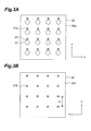
- Fig. 4A and Fig. 4B are plan views respectively showing the arrangement of (A) a signal input surface and (B) a signal output surface of a second wiring substrate.
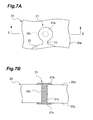
- each conductive member 26 is arranged by a conducting portion 26c, which is formed in the interior of a through hole 25c, an input portion 26a, which is formed on input surface 25a at an outer peripheral portion of through hole 25c so as to be continuous with conducting portion 26c, and an output portion 26b, which is formed on output surface 25b at an outer peripheral portion of through hole 25c so as to be continuous with conducting portion 26c.
- Fig. 6A and Fig. 6B are drawings showing an example of the arrangement of a conductive member provided in a through hole of a wiring substrate, with Fig. 6A being a top view and Fig. 6B being a section taken on arrows I-I.
- the arrangement of a conductive member 21, which is a conduction path, is illustrated using first wiring substrate 20 (see Fig. 3A and Fig. 3B) as an example.
Landscapes
- Physics & Mathematics (AREA)
- Health & Medical Sciences (AREA)
- Life Sciences & Earth Sciences (AREA)
- General Physics & Mathematics (AREA)
- High Energy & Nuclear Physics (AREA)
- Molecular Biology (AREA)
- Spectroscopy & Molecular Physics (AREA)
- Measurement Of Radiation (AREA)
- Solid State Image Pick-Up Elements (AREA)
- Transforming Light Signals Into Electric Signals (AREA)
- Light Receiving Elements (AREA)
Abstract
Description
Claims (9)
- A wiring substrate, having a conduction path that guide an electrical signal between a signal input surface and a signal output surface,
the wiring substrate comprising at least a first wiring substrate, disposed at the signal input surface side, and a second wiring substrate, connected to the first wiring substrate at the signal output surface side, each wiring substrate respectively comprising a glass substrate, formed of a predetermined glass material having a radiation shielding function and provided with a through hole, and a conductive member, disposed in the through hole and functioning as the conduction path by providing electrical continuity between the input surface and the output surface, and
wherein in the view in the conduction direction from the signal input surface to the signal output surface, the position of the through hole in the first wiring substrate differs from the position of the through hole in the second wiring substrate. - The wiring substrate according to Claim 1, wherein each of the first wiring substrate and the second wiring substrate is formed of the glass material that contains lead.
- The wiring substrate according to Claim 1 or 2, wherein the conductive member of each of the first wiring substrate and second wiring substrate is formed and disposed on the inner wall of the through hole that is provided in the glass substrate.
- The wiring substrate according to Claim 1 or 2, wherein the conductive member of each of the first wiring substrate and second wiring substrate is disposed by filling the interior of the through hole that is provided in the glass substrate.
- The wiring substrate according to any of Claims 1 through 4, wherein the glass substrate of each of the first wiring substrate and second wiring substrate is a glass substrate, wherein a plurality of the through holes are provided by fusing together and integrally forming a plurality of hollow glass members that are open at both ends.
- A radiation detector comprising:whrein the radiation detecting means, the wiring substrate section, and the signal processing means are positioned in that order along a predetermined alignment direction that substantially matches the conduction direction in the wiring substrate.a radiation detecting means, outputting a detected signal upon detecting radiation made incident thereon;a signal processing means, processing the detected signal from the radiation detecting means; anda wiring substrate section, having the wiring substrate according to any of Claims 1 through 5 that is provided with the conduction path that guide the detected signal between the signal input surface and the signal output surface, the radiation detecting means and the signal processing means being connected to the signal input surface and the signal output surface, respectively; and
- The radiation detector according to Claim 6, wherein the radiation detecting means comprises a scintillator, generating scintillation light upon incidence of radiation; and a semiconductor photodetecting element, detecting the scintillation light from the scintillator.
- The radiation detector according to Claim 6, wherein the radiation detecting means comprises a semiconductor detecting element, detecting radiation made incident thereon.
- The radiation detector according to any of Claims 6 through 8, wherein at least one of either the combination of the wiring substrate section and the radiation detecting means or the combination of the wiring substrate section and the signal processing means is electrically connected via a bump electrode.
Applications Claiming Priority (3)
| Application Number | Priority Date | Filing Date | Title |
|---|---|---|---|
| JP2003002541A JP4364514B2 (en) | 2003-01-08 | 2003-01-08 | Wiring board and radiation detector using the same |
| JP2003002541 | 2003-01-08 | ||
| PCT/JP2004/000079 WO2004064163A1 (en) | 2003-01-08 | 2004-01-08 | Wiring substrate and radiation detector using same |
Publications (3)
| Publication Number | Publication Date |
|---|---|
| EP1589582A1 true EP1589582A1 (en) | 2005-10-26 |
| EP1589582A4 EP1589582A4 (en) | 2007-02-14 |
| EP1589582B1 EP1589582B1 (en) | 2008-10-08 |
Family
ID=32708868
Family Applications (1)
| Application Number | Title | Priority Date | Filing Date |
|---|---|---|---|
| EP04700774A Expired - Lifetime EP1589582B1 (en) | 2003-01-08 | 2004-01-08 | Wiring substrate and radiation detector using same |
Country Status (9)
| Country | Link |
|---|---|
| US (1) | US20060244153A1 (en) |
| EP (1) | EP1589582B1 (en) |
| JP (1) | JP4364514B2 (en) |
| KR (1) | KR20050090133A (en) |
| CN (1) | CN100407432C (en) |
| DE (1) | DE602004016956D1 (en) |
| IL (1) | IL169586A0 (en) |
| TW (1) | TWI307556B (en) |
| WO (1) | WO2004064163A1 (en) |
Cited By (4)
| Publication number | Priority date | Publication date | Assignee | Title |
|---|---|---|---|---|
| EP1598862A4 (en) * | 2003-02-24 | 2006-12-06 | Hamamatsu Photonics Kk | SEMICONDUCTOR DEVICE AND RADIATION DETECTOR COMPRISING THIS DEVICE |
| EP1598863A4 (en) * | 2003-02-27 | 2006-12-13 | Hamamatsu Photonics Kk | SEMICONDUCTOR DEVICE AND RADIATION DETECTOR USING THE SAME |
| WO2007117799A2 (en) | 2006-03-30 | 2007-10-18 | Koninklijke Philips Electronics, N.V. | Radiation detector array |
| EP1653515B1 (en) * | 2004-10-26 | 2008-02-13 | Sony Corporation | Semiconductor image sensor module, method for manufacturing the same as well as camera and method for manufacturing the same |
Families Citing this family (14)
| Publication number | Priority date | Publication date | Assignee | Title |
|---|---|---|---|---|
| JP4365108B2 (en) * | 2003-01-08 | 2009-11-18 | 浜松ホトニクス株式会社 | Wiring board and radiation detector using the same |
| JP4133429B2 (en) | 2003-02-24 | 2008-08-13 | 浜松ホトニクス株式会社 | Semiconductor device |
| JP4421209B2 (en) * | 2003-04-11 | 2010-02-24 | 浜松ホトニクス株式会社 | Radiation detector |
| JP4451864B2 (en) * | 2006-07-11 | 2010-04-14 | 浜松ホトニクス株式会社 | Wiring board and solid-state imaging device |
| US7504637B2 (en) * | 2006-07-11 | 2009-03-17 | Aeroflex Colorado Springs Inc. | Two component photodiode detector |
| JP2010171307A (en) * | 2009-01-26 | 2010-08-05 | Panasonic Corp | Imaging device |
| JP2010212481A (en) * | 2009-03-11 | 2010-09-24 | Panasonic Corp | Imaging device |
| JP5358509B2 (en) | 2010-04-15 | 2013-12-04 | 浜松ホトニクス株式会社 | Radiation detector module |
| US8659148B2 (en) * | 2010-11-30 | 2014-02-25 | General Electric Company | Tileable sensor array |
| JP5901169B2 (en) * | 2011-07-26 | 2016-04-06 | キヤノン株式会社 | Scintillator structure and radiation detector |
| JP6285577B2 (en) * | 2015-01-15 | 2018-02-28 | コーニンクレッカ フィリップス エヌ ヴェKoninklijke Philips N.V. | Imaging detector module assembly |
| JP2016206101A (en) * | 2015-04-27 | 2016-12-08 | ソニー株式会社 | Radiation detection apparatus, imaging apparatus, and imaging system |
| JP6712215B2 (en) * | 2016-11-11 | 2020-06-17 | 浜松ホトニクス株式会社 | Photo detector |
| JP7500876B2 (en) * | 2020-11-13 | 2024-06-17 | エイエムエス-オスラム アーゲー | Modular assembly for the detection of X-ray radiation - Patents.com |
Family Cites Families (19)
| Publication number | Priority date | Publication date | Assignee | Title |
|---|---|---|---|---|
| US5043582A (en) * | 1985-12-11 | 1991-08-27 | General Imagining Corporation | X-ray imaging system and solid state detector therefor |
| FR2627923B1 (en) * | 1988-02-26 | 1990-06-22 | Thomson Csf | MATRIX OF PHOTOSENSITIVE ELEMENTS AND RADIATION DETECTOR COMPRISING SUCH A MATRIX, IN PARTICULAR A DOUBLE ENERGY X-RAY DETECTOR |
| US5187380A (en) * | 1992-04-09 | 1993-02-16 | General Electric Company | Low capacitance X-ray radiation detector |
| US5477933A (en) * | 1994-10-24 | 1995-12-26 | At&T Corp. | Electronic device interconnection techniques |
| JPH1056040A (en) * | 1996-08-08 | 1998-02-24 | Hitachi Ltd | Semiconductor device and manufacturing method thereof |
| CN100433305C (en) * | 1996-09-12 | 2008-11-12 | 揖斐电株式会社 | Substrates for mounting circuit components |
| US6620731B1 (en) * | 1997-12-18 | 2003-09-16 | Micron Technology, Inc. | Method for fabricating semiconductor components and interconnects with contacts on opposing sides |
| JP4693297B2 (en) * | 2000-08-10 | 2011-06-01 | キヤノン株式会社 | Radiation imaging apparatus and radiation imaging system |
| US6800857B2 (en) * | 2000-08-10 | 2004-10-05 | Canon Kabushiki Kaisha | Large-area fiber plate, radiation image pickup apparatus utilizing the same and producing method therefor |
| JP4012375B2 (en) * | 2001-05-31 | 2007-11-21 | 株式会社ルネサステクノロジ | Wiring board and manufacturing method thereof |
| CN1185915C (en) * | 2001-06-13 | 2005-01-19 | 佳能株式会社 | Flexible substrate, semiconductor device, camera device and X-ray camera system |
| US6510195B1 (en) * | 2001-07-18 | 2003-01-21 | Koninklijke Philips Electronics, N.V. | Solid state x-radiation detector modules and mosaics thereof, and an imaging method and apparatus employing the same |
| JP4237966B2 (en) * | 2002-03-08 | 2009-03-11 | 浜松ホトニクス株式会社 | Detector |
| US7230247B2 (en) * | 2002-03-08 | 2007-06-12 | Hamamatsu Photonics K.K. | Detector |
| JP2003282849A (en) * | 2002-03-26 | 2003-10-03 | Canon Inc | Radiation detection device and method of manufacturing connection substrate for radiation detection device |
| US7379528B2 (en) * | 2003-01-06 | 2008-05-27 | Koninklijke Philips Electronics N.V. | Radiation detector with shielded electronics for computed tomography |
| JP4138529B2 (en) * | 2003-02-24 | 2008-08-27 | 浜松ホトニクス株式会社 | Semiconductor device and radiation detector using the same |
| JP4365108B2 (en) * | 2003-01-08 | 2009-11-18 | 浜松ホトニクス株式会社 | Wiring board and radiation detector using the same |
| JP4421209B2 (en) * | 2003-04-11 | 2010-02-24 | 浜松ホトニクス株式会社 | Radiation detector |
-
2003
- 2003-01-08 JP JP2003002541A patent/JP4364514B2/en not_active Expired - Fee Related
-
2004
- 2004-01-08 CN CN2004800020298A patent/CN100407432C/en not_active Expired - Fee Related
- 2004-01-08 US US10/541,618 patent/US20060244153A1/en not_active Abandoned
- 2004-01-08 TW TW093100397A patent/TWI307556B/en not_active IP Right Cessation
- 2004-01-08 KR KR1020057011684A patent/KR20050090133A/en not_active Ceased
- 2004-01-08 EP EP04700774A patent/EP1589582B1/en not_active Expired - Lifetime
- 2004-01-08 WO PCT/JP2004/000079 patent/WO2004064163A1/en not_active Ceased
- 2004-01-08 DE DE602004016956T patent/DE602004016956D1/en not_active Expired - Lifetime
-
2005
- 2005-07-07 IL IL169586A patent/IL169586A0/en not_active IP Right Cessation
Cited By (10)
| Publication number | Priority date | Publication date | Assignee | Title |
|---|---|---|---|---|
| EP1598862A4 (en) * | 2003-02-24 | 2006-12-06 | Hamamatsu Photonics Kk | SEMICONDUCTOR DEVICE AND RADIATION DETECTOR COMPRISING THIS DEVICE |
| US7545044B2 (en) | 2003-02-24 | 2009-06-09 | Hamamatsu Photonics K.K. | Semiconductor device and radiation detector employing it |
| EP1598863A4 (en) * | 2003-02-27 | 2006-12-13 | Hamamatsu Photonics Kk | SEMICONDUCTOR DEVICE AND RADIATION DETECTOR USING THE SAME |
| US7663113B2 (en) | 2003-02-27 | 2010-02-16 | Hamamatsu Photonics K.K. | Semiconductor device and radiation detector employing it |
| EP1653515B1 (en) * | 2004-10-26 | 2008-02-13 | Sony Corporation | Semiconductor image sensor module, method for manufacturing the same as well as camera and method for manufacturing the same |
| WO2007117799A2 (en) | 2006-03-30 | 2007-10-18 | Koninklijke Philips Electronics, N.V. | Radiation detector array |
| WO2007117799A3 (en) * | 2006-03-30 | 2007-12-06 | Koninkl Philips Electronics Nv | Radiation detector array |
| RU2408110C2 (en) * | 2006-03-30 | 2010-12-27 | Конинклейке Филипс Электроникс, Н.В. | Radiation detector array |
| US8710448B2 (en) | 2006-03-30 | 2014-04-29 | Koninklijke Philips N.V. | Radiation detector array |
| EP3361507A1 (en) * | 2006-03-30 | 2018-08-15 | Koninklijke Philips N.V. | Radiation detector array |
Also Published As
| Publication number | Publication date |
|---|---|
| CN1723565A (en) | 2006-01-18 |
| CN100407432C (en) | 2008-07-30 |
| WO2004064163A1 (en) | 2004-07-29 |
| US20060244153A1 (en) | 2006-11-02 |
| JP2004265884A (en) | 2004-09-24 |
| EP1589582B1 (en) | 2008-10-08 |
| TWI307556B (en) | 2009-03-11 |
| DE602004016956D1 (en) | 2008-11-20 |
| KR20050090133A (en) | 2005-09-12 |
| TW200418195A (en) | 2004-09-16 |
| IL169586A0 (en) | 2007-07-04 |
| EP1589582A4 (en) | 2007-02-14 |
| JP4364514B2 (en) | 2009-11-18 |
Similar Documents
| Publication | Publication Date | Title |
|---|---|---|
| US7507971B2 (en) | Radioactive ray detector | |
| US7326907B2 (en) | Wiring substrate and radiation detector using same | |
| US7838994B2 (en) | Semiconductor device and radiation detector employing it | |
| EP1589582B1 (en) | Wiring substrate and radiation detector using same | |
| US7545044B2 (en) | Semiconductor device and radiation detector employing it | |
| US7663113B2 (en) | Semiconductor device and radiation detector employing it | |
| JP2008235929A (en) | Semiconductor device |
Legal Events
| Date | Code | Title | Description |
|---|---|---|---|
| PUAI | Public reference made under article 153(3) epc to a published international application that has entered the european phase |
Free format text: ORIGINAL CODE: 0009012 |
|
| 17P | Request for examination filed |
Effective date: 20050729 |
|
| AK | Designated contracting states |
Kind code of ref document: A1 Designated state(s): AT BE BG CH CY CZ DE DK EE ES FI FR GB GR HU IE IT LI LU MC NL PT RO SE SI SK TR |
|
| AX | Request for extension of the european patent |
Extension state: AL LT LV MK |
|
| DAX | Request for extension of the european patent (deleted) | ||
| RBV | Designated contracting states (corrected) |
Designated state(s): DE FR GB NL |
|
| A4 | Supplementary search report drawn up and despatched |
Effective date: 20070116 |
|
| RIC1 | Information provided on ipc code assigned before grant |
Ipc: G01T 1/20 20060101ALI20070109BHEP Ipc: G01T 1/24 20060101ALI20070109BHEP Ipc: H01L 27/146 20060101AFI20041011BHEP |
|
| 17Q | First examination report despatched |
Effective date: 20070423 |
|
| GRAP | Despatch of communication of intention to grant a patent |
Free format text: ORIGINAL CODE: EPIDOSNIGR1 |
|
| GRAS | Grant fee paid |
Free format text: ORIGINAL CODE: EPIDOSNIGR3 |
|
| GRAA | (expected) grant |
Free format text: ORIGINAL CODE: 0009210 |
|
| AK | Designated contracting states |
Kind code of ref document: B1 Designated state(s): DE FR GB NL |
|
| REG | Reference to a national code |
Ref country code: GB Ref legal event code: FG4D |
|
| REF | Corresponds to: |
Ref document number: 602004016956 Country of ref document: DE Date of ref document: 20081120 Kind code of ref document: P |
|
| PLBE | No opposition filed within time limit |
Free format text: ORIGINAL CODE: 0009261 |
|
| STAA | Information on the status of an ep patent application or granted ep patent |
Free format text: STATUS: NO OPPOSITION FILED WITHIN TIME LIMIT |
|
| 26N | No opposition filed |
Effective date: 20090709 |
|
| PGFP | Annual fee paid to national office [announced via postgrant information from national office to epo] |
Ref country code: FR Payment date: 20120202 Year of fee payment: 9 |
|
| PGFP | Annual fee paid to national office [announced via postgrant information from national office to epo] |
Ref country code: DE Payment date: 20120104 Year of fee payment: 9 |
|
| PGFP | Annual fee paid to national office [announced via postgrant information from national office to epo] |
Ref country code: GB Payment date: 20120104 Year of fee payment: 9 |
|
| PGFP | Annual fee paid to national office [announced via postgrant information from national office to epo] |
Ref country code: NL Payment date: 20120125 Year of fee payment: 9 |
|
| REG | Reference to a national code |
Ref country code: NL Ref legal event code: V1 Effective date: 20130801 |
|
| GBPC | Gb: european patent ceased through non-payment of renewal fee |
Effective date: 20130108 |
|
| REG | Reference to a national code |
Ref country code: FR Ref legal event code: ST Effective date: 20130930 |
|
| PG25 | Lapsed in a contracting state [announced via postgrant information from national office to epo] |
Ref country code: NL Free format text: LAPSE BECAUSE OF NON-PAYMENT OF DUE FEES Effective date: 20130801 Ref country code: DE Free format text: LAPSE BECAUSE OF NON-PAYMENT OF DUE FEES Effective date: 20130801 |
|
| REG | Reference to a national code |
Ref country code: DE Ref legal event code: R119 Ref document number: 602004016956 Country of ref document: DE Effective date: 20130801 |
|
| PG25 | Lapsed in a contracting state [announced via postgrant information from national office to epo] |
Ref country code: FR Free format text: LAPSE BECAUSE OF NON-PAYMENT OF DUE FEES Effective date: 20130131 Ref country code: GB Free format text: LAPSE BECAUSE OF NON-PAYMENT OF DUE FEES Effective date: 20130108 |