EP1589379A2 - Optical illumination system, exposure apparatus and device fabrication method - Google Patents
Optical illumination system, exposure apparatus and device fabrication method Download PDFInfo
- Publication number
- EP1589379A2 EP1589379A2 EP05252521A EP05252521A EP1589379A2 EP 1589379 A2 EP1589379 A2 EP 1589379A2 EP 05252521 A EP05252521 A EP 05252521A EP 05252521 A EP05252521 A EP 05252521A EP 1589379 A2 EP1589379 A2 EP 1589379A2
- Authority
- EP
- European Patent Office
- Prior art keywords
- light
- optical system
- target surface
- optical
- illumination optical
- Prior art date
- Legal status (The legal status is an assumption and is not a legal conclusion. Google has not performed a legal analysis and makes no representation as to the accuracy of the status listed.)
- Withdrawn
Links
- 230000003287 optical effect Effects 0.000 title claims abstract description 229
- 238000005286 illumination Methods 0.000 title claims abstract description 96
- 238000000034 method Methods 0.000 title claims description 25
- 238000004519 manufacturing process Methods 0.000 title claims description 15
- 230000010287 polarization Effects 0.000 claims abstract description 42
- 239000000463 material Substances 0.000 claims abstract description 30
- 239000011521 glass Substances 0.000 claims abstract description 26
- 230000008569 process Effects 0.000 claims description 15
- 210000001747 pupil Anatomy 0.000 claims description 13
- 239000000758 substrate Substances 0.000 claims description 12
- 230000005465 channeling Effects 0.000 claims description 7
- 238000011161 development Methods 0.000 claims description 5
- 239000010408 film Substances 0.000 description 14
- 239000004065 semiconductor Substances 0.000 description 11
- 238000002834 transmittance Methods 0.000 description 10
- 238000009826 distribution Methods 0.000 description 9
- 230000000873 masking effect Effects 0.000 description 9
- 230000007423 decrease Effects 0.000 description 8
- 230000008859 change Effects 0.000 description 7
- 238000000206 photolithography Methods 0.000 description 5
- 229920002120 photoresistant polymer Polymers 0.000 description 4
- 238000007493 shaping process Methods 0.000 description 4
- 230000005540 biological transmission Effects 0.000 description 3
- WUKWITHWXAAZEY-UHFFFAOYSA-L calcium difluoride Chemical compound [F-].[F-].[Ca+2] WUKWITHWXAAZEY-UHFFFAOYSA-L 0.000 description 3
- 238000013461 design Methods 0.000 description 3
- 238000010586 diagram Methods 0.000 description 3
- 238000003384 imaging method Methods 0.000 description 3
- 238000002310 reflectometry Methods 0.000 description 3
- 238000012360 testing method Methods 0.000 description 3
- XUIMIQQOPSSXEZ-UHFFFAOYSA-N Silicon Chemical compound [Si] XUIMIQQOPSSXEZ-UHFFFAOYSA-N 0.000 description 2
- 229910001634 calcium fluoride Inorganic materials 0.000 description 2
- 238000001444 catalytic combustion detection Methods 0.000 description 2
- 238000005530 etching Methods 0.000 description 2
- 238000005389 semiconductor device fabrication Methods 0.000 description 2
- 229910052710 silicon Inorganic materials 0.000 description 2
- 239000010703 silicon Substances 0.000 description 2
- 240000006829 Ficus sundaica Species 0.000 description 1
- 230000004075 alteration Effects 0.000 description 1
- 230000008901 benefit Effects 0.000 description 1
- 230000015572 biosynthetic process Effects 0.000 description 1
- 230000005684 electric field Effects 0.000 description 1
- 239000007943 implant Substances 0.000 description 1
- 230000006872 improvement Effects 0.000 description 1
- 238000007689 inspection Methods 0.000 description 1
- 238000005468 ion implantation Methods 0.000 description 1
- 150000002500 ions Chemical class 0.000 description 1
- 230000001678 irradiating effect Effects 0.000 description 1
- 239000004973 liquid crystal related substance Substances 0.000 description 1
- 238000001459 lithography Methods 0.000 description 1
- 239000000203 mixture Substances 0.000 description 1
- 238000012986 modification Methods 0.000 description 1
- 230000004048 modification Effects 0.000 description 1
- 230000003647 oxidation Effects 0.000 description 1
- 238000007254 oxidation reaction Methods 0.000 description 1
- 238000004806 packaging method and process Methods 0.000 description 1
- 238000007789 sealing Methods 0.000 description 1
- 239000010409 thin film Substances 0.000 description 1
- 238000013519 translation Methods 0.000 description 1
Images


Classifications
-
- G—PHYSICS
- G03—PHOTOGRAPHY; CINEMATOGRAPHY; ANALOGOUS TECHNIQUES USING WAVES OTHER THAN OPTICAL WAVES; ELECTROGRAPHY; HOLOGRAPHY
- G03F—PHOTOMECHANICAL PRODUCTION OF TEXTURED OR PATTERNED SURFACES, e.g. FOR PRINTING, FOR PROCESSING OF SEMICONDUCTOR DEVICES; MATERIALS THEREFOR; ORIGINALS THEREFOR; APPARATUS SPECIALLY ADAPTED THEREFOR
- G03F7/00—Photomechanical, e.g. photolithographic, production of textured or patterned surfaces, e.g. printing surfaces; Materials therefor, e.g. comprising photoresists; Apparatus specially adapted therefor
- G03F7/70—Microphotolithographic exposure; Apparatus therefor
- G03F7/708—Construction of apparatus, e.g. environment aspects, hygiene aspects or materials
- G03F7/7095—Materials, e.g. materials for housing, stage or other support having particular properties, e.g. weight, strength, conductivity, thermal expansion coefficient
- G03F7/70958—Optical materials or coatings, e.g. with particular transmittance, reflectance or anti-reflection properties
- G03F7/70966—Birefringence
-
- G—PHYSICS
- G03—PHOTOGRAPHY; CINEMATOGRAPHY; ANALOGOUS TECHNIQUES USING WAVES OTHER THAN OPTICAL WAVES; ELECTROGRAPHY; HOLOGRAPHY
- G03F—PHOTOMECHANICAL PRODUCTION OF TEXTURED OR PATTERNED SURFACES, e.g. FOR PRINTING, FOR PROCESSING OF SEMICONDUCTOR DEVICES; MATERIALS THEREFOR; ORIGINALS THEREFOR; APPARATUS SPECIALLY ADAPTED THEREFOR
- G03F7/00—Photomechanical, e.g. photolithographic, production of textured or patterned surfaces, e.g. printing surfaces; Materials therefor, e.g. comprising photoresists; Apparatus specially adapted therefor
- G03F7/70—Microphotolithographic exposure; Apparatus therefor
- G03F7/70058—Mask illumination systems
- G03F7/70191—Optical correction elements, filters or phase plates for controlling intensity, wavelength, polarisation, phase or the like
-
- G—PHYSICS
- G03—PHOTOGRAPHY; CINEMATOGRAPHY; ANALOGOUS TECHNIQUES USING WAVES OTHER THAN OPTICAL WAVES; ELECTROGRAPHY; HOLOGRAPHY
- G03F—PHOTOMECHANICAL PRODUCTION OF TEXTURED OR PATTERNED SURFACES, e.g. FOR PRINTING, FOR PROCESSING OF SEMICONDUCTOR DEVICES; MATERIALS THEREFOR; ORIGINALS THEREFOR; APPARATUS SPECIALLY ADAPTED THEREFOR
- G03F7/00—Photomechanical, e.g. photolithographic, production of textured or patterned surfaces, e.g. printing surfaces; Materials therefor, e.g. comprising photoresists; Apparatus specially adapted therefor
- G03F7/70—Microphotolithographic exposure; Apparatus therefor
- G03F7/70483—Information management; Active and passive control; Testing; Wafer monitoring, e.g. pattern monitoring
- G03F7/7055—Exposure light control in all parts of the microlithographic apparatus, e.g. pulse length control or light interruption
- G03F7/70566—Polarisation control
-
- G—PHYSICS
- G07—CHECKING-DEVICES
- G07D—HANDLING OF COINS OR VALUABLE PAPERS, e.g. TESTING, SORTING BY DENOMINATIONS, COUNTING, DISPENSING, CHANGING OR DEPOSITING
- G07D9/00—Counting coins; Handling of coins not provided for in the other groups of this subclass
Definitions
- the present invention relates generally to an illumination optical system for illuminating a target surface with light from a light source, an exposure apparatus, and a device fabrication method, and more particularly to an illumination optical system for illuminating a reticle (or a mask) which forms a pattern with short wavelength light.
- the present invention is suitable for a projection exposure apparatus used in a photolithography process for fabricating semiconductor devices, liquid crystal display devices, image pick-up devices (CCD, and the like), thin-film magnetic heads, and the like.
- the photolithography process is a process of projection transcribing a circuit pattern of the semiconductor device on a substrate (silicon substrate, and the like) that becomes the semiconductor device.
- Minute semiconductor devices have been increasingly demanded.
- the minimum line width of a line and space demanded is 0.15 ⁇ m or less, and reaching 0.10 ⁇ m.
- the improvement of a resolution of the projection optical system used for the photolithography process is necessary to create minute semiconductors.
- the line width R that can be resolved decreases in proportion to wavelength.
- the numerical aperture NA is increased, the line width R that can be resolved decreases in inverse proportion to numerical aperture.
- the exposure light source of the current mainstream projection exposure apparatus is KrF excimer laser with a wavelength of 248 nm.
- the current mainstream NA is about 0.80, but the projection exposure apparatus that is developed has NA of 0.90.
- a glass material with high transmittance is limited to the short wavelength of the light source, and a glass material that can be used by the wavelength of 157 nm is only a calcium fluoride (CaF 2 ) at present.
- CaF 2 calcium fluoride
- An optical system that uses a 45° mirror is proposed as an example of the catadioptric system as shown in FIG. 5 (see, for example, Japanese translation of PCT international Application Publication No. 7-111512).
- the reflectivity of the 45° mirror is different in S-polarized light (a light beam whose direction of electric field vector is vertical to a normal of a reflection surface and traveling direction of the light beam) and P-polarized light (an orthogonal light beam to the s-polarized light). Therefore, the transmittance between the reticle and the wafer is different between the light beam that becomes p-polarized light and the light beam that becomes s-polarized light for the mirror in the catadioptric system.
- a contrast of an interference fringe that the line and space of the reticle forms on a photoresist on the wafer is known as follows: S-polarized light has higher contrast than P-polarized light for a diffraction light of the line and space.
- the contrast changes depending on the pattern direction.
- FIG. 6 A situation that applies a reticle to form a pattern repeated in y direction to the optical system shown in FIG. 5, is shown in FIG. 6.
- FIGs. 7A and 7B A situation that applies a reticle to form a pattern repeated in x direction to the optical system shown in FIG. 5 is shown in FIGs. 7A and 7B.
- a diffraction light of the repeated pattern in the y direction shown in FIG. 6 is reflected to the x direction, and s-polarized light component of the diffraction light becomes s-polarized light component for the mirror.
- a diffraction light of the repeated pattern in the x direction shown in FIG. 7 is reflected to the y direction, and s-polarized light component of the diffraction light becomes p-polarized light component for the mirror.
- the reflectivity of the mirror is different in S-polarized light component and P-polarized light component, So S-polarized light component of the diffraction light diffracted by each of the repeated patterns shown in FIG. 6 and the repeated patterns shown in FIG. 7 becomes S-polarized light and P-polarized light respectively for the mirror, and a transmittance that transmits the projection optical system is different.
- a transmittance that is composed of S-polarized light component and P-polarized light component does not depend on the pattern and is constant, and a light intensity ratio of S- polarized light component and P-polarized light component of the diffraction light that reaches the wafer is different depending on the pattern direction.
- the contrast is different in S-polarized light component and P-polarized light component. If the same light intensity as light intensity of S-polarized light and P-polarized light illuminates the reticle, the contrast difference, that depends upon the pattern direction, is caused in the projection exposure apparatus that uses the projection optical system of the catadioptric system.
- the polarized light state changes by a birefringence generated by a birefringence of the glass material of the illumination optical system until the reticle surface and a stress that given the lens when lens is fixoduntil the stress is reduced to produce the predetermined ratio.
- FIG. 8 shows a calculation result that the light of S-polarized light at the pupil position of the illumination optical system change into the light intensity distribution (of S-polarized light and P-polarized light) at the reticle surface.
- This illumination optical system has an optical system that adjusts the polarization ratio at the pupil position, is used for the light source of light with a wavelength of 157 nm, and a calcium fluoride that has birefringence amount of 2 nm/cm on m+2s (m: average, s: variance) is used as a lens of the illumination optical system.
- a thickness of the glass material from the pupil position of the illumination optical system to the reticle is about 500 mm, and a number of lens is 15.
- the right side drawing is a pupil distribution of P-polarized light at a predetermined point on the reticle surface.
- the S-polarized light might change into P-polarized light by the birefringence of the lens even in case of incidence. For example, when the birefringence of the calcium fluoride is 2 nm/cm, maximum 25 % P-polarized light is generated at the reticle surface.
- FIG. 9 shows a relationship between a birefringence amount of the glass material used for the illumination optical system lens and the maximum P-polarized light intensity in a pupil of the reticle surface made by light of S-polarized light at pupil position of the illumination system.
- Plural points in the same birefringence amount is one that a built-in angle of lens to a lens barrel was changed, and the maximum P-polarized light intensity in the pupil in the reticle surface changes by combining a phase advance axis.
- the ratio of S-polarized light changing into P-polarized light increases as the birefringence amount increasesas shown on graph on Fig.9.
- the light of 90 % of S-polarized light at the pupil position of the illumination optical system might change into the P-polarized light.
- an exemplary object to provide an illumination optical system that can achieve a desired polarized light illumination on a reticle surface.
- An illumination optical system of one aspect according to the present invention for illuminating a target surface using light from a light source includes a polarizing element that arranged in an optical path from the light source to the target surface, and adjusts a polarization ratio of the light, and an optical element that is arranged in an optical path from the polarizing element to the target surface, characterized in that the optical element is m+2s ⁇ 1.0 nm/cm, where an average of birefringence amount of a glass material of the optical element is m, and standard variation birefringence amount of a glass material of the optical element is s.
- An illumination optical system of another aspect according to the present invention for illuminating a target surface using light from a light source includes a polarizing element that is arranged in an optical path from the light source to the target surface, and adjusts a polarization ratio of the light, characterized in that an optical element that has power is not arranged in an optical path from the polarizing element to the target surface.
- An exposure apparatus of another aspect according to the present invention includes an illumination optical system for illuminating a target surface using light from a light source, and a projection optical system for channeling the light that passes through the target surface onto a substrate, wherein the illumination optical system includes a polarizing element that is arranged in an optical path from the light source to the target surface, and adjusts a polarization ratio of the light, and an optical element that is arranged in an optical path from the polarizing element to the target surface, characterized in that the optical element is m+2s ⁇ 1.0 nm/cm, where an average of birefringence amount of a glass material of the optical element is m, and standard variation birefringence amount of a glass material of the optical element is s.
- An exposure apparatus of another aspect according to the present invention includes an illumination optical system for illuminating a target surface using light from a light source, and a projection optical system for channeling the light that passes through the target surface onto a substrate, wherein the illumination optical system includes a polarizing element that is arranged in an optical path from the light source to the target surface, which adjusts a polarization ratio of the light, characterized in that an optical element that has power is not arranged in an optical path from the polarizing element to the target surface.
- a device fabrication method of another aspect according to the present invention includes the steps of exposing an object using an exposure apparatus, and performing a development process for the object exposed, and manufacturing a device from the exposed object
- the exposure apparatus includes an illumination optical system for illuminating a target surface using light from a light source, and a projection optical system for channeling the light that passes through the target surface onto a substrate
- the illumination optical system includes a polarizing element that is arranged in an optical path from the light source to the target surface, and adjusts a polarization ratio of the light, and an optical element that is arranged in an optical path from the polarizing element to the target surface, characterized in that the optical element is m+2s ⁇ 1.0 nm/cm, where an average of birefringence amount of a glass material of the optical element is m, and standard variation birefringence amount of a glass material of the optical element is s.
- a device fabrication method of another aspect according to the present invention includes the steps of exposing an object using an exposure apparatus, and performing a development process for the object exposed, and manufacturing a device from the exposed object, wherein the exposure apparatus includes an illumination optical system for illuminating a target surface using light from a light source, and a projection optical system for channeling the light that passes through the target surface onto a substrate, wherein the illumination optical system includes a polarizing element that is arranged in an optical path from the light source to the target surface, and adjusts a polarization ratio of the light, characterized in that an optical element that has power is not arranged in an optical path from the polarizing element to the target surface.
- FIG. 1 is a schematic structure view of an exposure apparatus S that includes the illumination optical system of the instant embodiment.
- a light source 1 uses KrF excimer laser, ArF excimer laser, or F 2 laser etc.
- a beam shaping optical system 2 channels a light from the light source 1, and forms a desired light intensity distribution on a fly-eye lens 4.
- a polarizing element 3 adjusts a polarization ratio to be a predetermined polarization ratio at a reticle 10 surface (target surface).
- the fly-eye lens 4 wavefront-divides the light from the light source 1, and forms a plural secondary light source.
- a condenser lens 5 overlaps light from the secondary light source formed by the fly-eye lens 4 to the masking blade 6. Thereby, a uniformly light intensity distribution is obtained.
- a lens 7 and a lens 9 as an optical element are a relay optical system, and form a conjugate relationship between the masking blade 6 and the reticle 10 by reflecting the light that passes through the masking blade 6 as an optical element at a folding mirror 8. If an incident angle differs greatly from 45° when reflecting by the folding mirror 8, a phase difference between the light of P-polarized light and the light of S-polarized light for the mirror is generated by a dielectric reflection film formed on the mirror, and the polarized light state collapses. Then, the incident angle to the folding mirror 8 may be within 45° ⁇ 30°.
- a dielectric transmission film generates the phase difference that is smaller than the phase difference on the reflection film by the polarized light when greatly inclining towards the surface. Therefore, the incident light to the lens and the exit light from the lens may be within 0° ⁇ 50°.
- the illumination optical system is composed of the items from the beam shaping optical system 2 to the lens 9 just before the reticle 10, and the illumination optical system and the light source 1 compose the illumination optical apparatus.
- a projection optical system 11 projects a pattern of the reticle 10 onto a wafer (substrate) 12 onto which the photoresist is applied.
- the present invention adjusts the birefringence of an optical member on an optical path from the polarizing element 3 to the reticle 10 to 1 nm/cm or less on m+2s to maintain the polarization ratio formed by the polarizing element 3 and illuminates the reticle 10. Therefore, the change of the polarization ratio can be suppressed to 10 % or less as shown in FIG. 9 , and an enough imaging performance can be obtained.
- the polarizing element 3 is composed of one or more inclined surfaces to the optical path that has a dielectric multilayer film inclined to the optical path.
- the surface is vertical to the optical path (in other words, an optical axis)
- An incline angle of the surface may be between 15° and 65° in the film design.
- the dielectric multilayer film (as follows “dielectric film”) is formed by two surfaces it may be formed in the shape of an inverted “V", or the Japanese “ / ⁇ " character, in the vertical direction on the optical axis by inclining two surfaces in the opposite direction to equate the polarized light characteristic of upward light ray and a downward light ray for the optical axis (reference to FIG. 1) .
- the angle of the light ray that is incident onto the polarizing element 3 the transmittance or reflectivity of S-polarized light and P-polarized light changes. Then, a light intensity bary-center of a light group that is incident onto each point of the polarizing element 3 may be parallel to the optical axis.
- the polarizing element 3 that adjusts the polarization ratio by the dielectric film uses a transmission type, and may use a reflection type element.
- the polarization ratio is adjusted by the dielectric film, unnecessary light is diffused outside of the optical path by the reflection or transmission and the light intensity is adjusted to achieve the desired polarization ratio.
- the light intensity on the wafer surface decreases, and the throughput decreases. Therefore, when a pattern that is transferred is not influenced by the HV difference of the polarized light, it is desirable to expose with high intensity light without inserting the polarizing element.
- the light source 1 uses KrF excimer laser, ArF excimer laser, or F 2 laser etc.
- the beam shaping optical system 2 leads the light from the light source 1, and forms the desired light intensity distribution on the fly-eye lens 4.
- the polarizing element 3 adjusts the polarization ratio to be the predetermined polarization ratio at the reticle 10 surface.
- the fly-eye lens 4 wavefront-divides the light from the light source 1, and forms the plural secondary light source.
- the condenser lens 5 overlaps light from the secondary light source formed by the fly-eye lens 4 to the masking blade 6. Thereby, the uniformly light intensity distribution is obtained.
- the lens 7 and the lens 9 are the relay optical system, and form the conjugate relationship between the masking blade 6 and the reticle 10 by reflecting the light that passes through the masking blade 6 at the folding mirror 8.
- the illumination optical system is composed of items from the light source 1 to the lens 9 just before the reticle 10.
- the projection optical system 11 projects the pattern of the reticle 10 onto the wafer 12 that the photoresist is applied.
- the polarization ratio that the polarizing element 3 should adjust depends on the birefringence amount that changes between the polarizing element 3 and the reticle 10. For example, the following are assumed: the birefringence amount of the optical member from the polarizing element 3 to the reticle 10 surface is 2 nm/cm, 25% of S-polarized light is converted into P-polarized light, and 25% of P-polarized light is converted into S-polarized light.
- the polarization ratio that the polarizing element 3 adjusts may be decided so that the average polarization ratio in the pupil becomes the desired value.
- the amount of polarized light from the polarizing element 3 to the reticle 10 surface changes when the birefringence of the optical member changes by continuously irradiating light when NA of the illumination system is changed or the illumination area is changed.
- the instant embodiment enables the exchange of two polarizing elements 31 and 32 that have a different characteristic as shown in FIG. 2, and when the rate that the polarized light changes between from the polarizing element 3 to the reticle 10 surface changes, those polarizing elements are exchanged.
- the polarizing elements that can be exchanged are not limited to two, and may be three or more.
- the polarizing elements are not exchanged, and the polarized light may be continuously changed by changing the incline angle of the surface of the polarizing element.
- a polarized light monitor (not shown) that measures a light intensity ratio of S-polarized light and P-polarized light is installed in a wafer stage, the polarized light monitor is inserted in the wafer 12 surface and the polarized light state is detected, and the polarization ratio may be adjusted so that the light intensity ratio of S-polarized light and P-polarized light becomes the desired ratio.
- FIG. 3 is a schematic structure view of an exposure apparatus S that includes the illumination optical system of the instant embodiment.
- the light source 1 uses KrF excimer laser, ArF excimer laser, or F 2 laser etc.
- a random polarized plate 15 polarizes the light from the light source 1 in two orthogonal directions, and forms two light beams from a random polarized light of the light intensity ratio of 1 : 1.
- the random polarized plate 15 uses a parallel flat plate that stacks a sphenoid member formed from a birefringent material and a sphenoid member formed from a non-birefringent material.
- the beam shaping optical system 2 channels the light from the light source 1, and forms the desired light intensity distribution on the fly-eye lens 4.
- the fly-eye lens 4 wavefront-divides the light from the light source 1, and forms the plural secondary light source.
- the condenser lens 5 overlaps light from the secondary light source formed by the fly-eye lens 4 to the masking blade 6. Thereby, the uniformly light intensity distribution is obtained.
- the lens 7 and the lens 9 are the relay optical system, and form the conjugate relationship between the masking blade 6 and the reticle 10 by reflecting the light that passes through the masking blade 6 at the folding mirror 8.
- the polarizing element 3 adjusts the polarization ratio to be the predetermined polarization ratio at the reticle 10 surface.
- the illumination optical system is composed of the light source 1 to the polarizing element 3 just before the reticle 10.
- the projection optical system 11 projects the pattern of the reticle 10 onto the wafer 12 that the photoresist is applied.
- the instant embodiment adjusts the polarization ratio just on the reticle 10 surface by the polarizing element 3 so as not to receive the influence of the birefringent optical member in the illumination system.
- the light intensity ratio of the S-polarized light and P-polarized light of the light that is incident onto the polarizing element 3 may be a random polarized light of 1 : 1.
- the random polarized light that the light intensity ratio of the S-polarized light and P-polarized light is 1 : 1 even when the polarized light state is changed by the optical member of the illumination system having the birefringence, the light amount that changes from S-polarized light into P-polarized light is equal to the light amount that changes from P-polarized light into S-polarized light. Therefore, the random polarized light, that the light intensity ratio of the S-polarized light and P-polarized light maintained to 1 1, is incident onto the polarizing element 3 without depending on the birefringence amount of the optical member.
- the random polarized light plate 15 converts the light from the light source 1 into the polarized light state so that the light intensity ratio of S-polarized light and S-polartzed light is the random polarized light of 1 : 1.
- the birefringence amount of the optical members from the light source to the polarizing element need not be considered by arranging the random polarized light plate, so the random polarized plate is arranged between the light source and the polarizing element in other embodiments.
- a ⁇ /4 plate may be used instead of the random polarized light plate.
- the reticle 10 surface as the target surface is, generally, illuminated using an illumination area of a rectangle shape that has short length direction and long length direction, elliptical shape, or segment shape. Then, the reticle is scanned along the short length direction.
- the third embodiment is a composition in which a surface of polarizing element where dielectric film is formed is inclined in the scanning direction of the projection exposure apparatus, in other words, the short length direction of the illumination area. Thereby, a space in the direction of the optical axis to insert the polarizing element in the optical path can be reduced.
- FIG. 4 is a schematic structure view of an exposure apparatus S that includes the illumination optical system of the instant embodiment.
- the structure of the fourth embodiment is the structure of the third embodiment shown in FIG. 3 in addition to a structure that a phase plate ( ⁇ /2 plate) 14 and parallel plane plate 13 can enable to locate on and remove from the optical path between the lens 9 and the reticle 10.
- FIG. 10 is a schematic structure view of an exposure apparatus S that includes the illumination optical system of the instant embodiment.
- the fifth embodiment decreases a light loss by changing the polarized state of the light source by a phase plate 16 which changes the predetermined polarized light state when the polarized light state of the light source is a predetermined state (for instant, linearly polarized light) to improve the problem of the first embodiment shown in FIG. 1.
- the first embodiement generates the light loss by leaking desired polarized light through the polarizing element's that consists of dielectric multilayer film.
- the illumination optical system of the fifth embodiment should maintain the polarized light state of the light source to the phase plate 16, as the polarizing element, and creates the birefringence of the optical member on the optical path from the light source to polarizing element of 1 nm/cm or less on m+2s. Therefore, the change in the polarization ratio can be suppressed to 10% or less as shown in FIG. 9, and an enough imaging performance can be obtained. Moreover, the loss of the light intensity is a little, and it is possible to illuminate the reticle by the high intensity light.
- FIG. 11 is a schematic structure view of an exposure apparatus S that includes the illumination optical system of the instant embodiment.
- the sixth embodiment is the structure of the fifth embodiment shown in FIG. 5 in addition to the polarization separating plate 3.
- the illumination optical system of the fifth embodiment should strictly maintain the polarized light state of the light source to the phase plate 16 as the polarizing element, and the birefringence of the optical member on the optical path from the light source to the polarizing element should be 1 nm/cm or less on m+2s.
- the sixth embodiment maintains the polarized light state of the light source, and removes unnecessary polarized light of the collapsed polarized light state by the polarization separating plate 3. Therefore, even if the birefringence of the optical member on the optical path from the light source to the polarizing element is allowed to 5 nm/cm or less on m+2s, the polarized light state of the light that is incidence onto the phase plate 16 can be maintained in the desired state.
- the polarized light state of the light that is incident onto the polarization separating plate is preserved compared with the first embodiment, so the light intensity that does not reach the target surface by the reflection decrease, and the light intensity loss decreases. Therefore, the change in the polarization ratio can be suppressed to 10% or less as shown in FIG. 9, and an enough imaging performance can be obtained. Moreover, the loss of the light intensity is a little, and it is possible to illuminate the reticle by the high intensity light.
- FIG. 12 is a flowchart for explaining how to fabricate devices (i.e., semiconductor chips such as IC and LSI, LCDs, CCDs, and the like).
- a description will be given of the fabrication of a semiconductor chip as an example.
- Step 101 circuit design
- Step 102 mask fabrication
- Step 103 wafer making
- Step 104 wafer process
- Step 105 assembly
- Step 106 inspection
- steps 107 performs various tests on the semiconductor device made in Step 105, such as a validity test and a durability test. Through these steps, a semiconductor device is finished and shipped (Step 107).
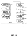
- FIG. 13 is a detailed flowchart of the wafer process in Step 104.
- Step 111 oxidation
- Step 112 CVD
- Step 113 electrode formation
- Step 114 ion implantation
- Step 115 resist process
- Step 116 exposure
- Step 117 development
- Step 118 etching
- Step 119 removes unused resist after etching. These steps are repeated to form multi-layer circuit patterns on the wafer.
- the fabrication method of the instant embodiment can fabricate higher-quality devices (in other words, the desired stroke width devices).
- the device fabrication method using the exposure apparatus S, and resultant devices constitute one aspect of the present invention.
- the present invention polarized light-illuminates using the illumination optical system that includes the glass material that has the birefringence, and can improve the resolution of the projection exposure apparatus.
- the illumination optical system can achieve the polarized light illumination on the reticle surface.
Landscapes
- Physics & Mathematics (AREA)
- General Physics & Mathematics (AREA)
- Health & Medical Sciences (AREA)
- Engineering & Computer Science (AREA)
- Environmental & Geological Engineering (AREA)
- Epidemiology (AREA)
- Public Health (AREA)
- Exposure And Positioning Against Photoresist Photosensitive Materials (AREA)
- Exposure Of Semiconductors, Excluding Electron Or Ion Beam Exposure (AREA)
- Microscoopes, Condenser (AREA)
- Polarising Elements (AREA)
Abstract
Description
- The present invention relates generally to an illumination optical system for illuminating a target surface with light from a light source, an exposure apparatus, and a device fabrication method, and more particularly to an illumination optical system for illuminating a reticle (or a mask) which forms a pattern with short wavelength light. The present invention is suitable for a projection exposure apparatus used in a photolithography process for fabricating semiconductor devices, liquid crystal display devices, image pick-up devices (CCD, and the like), thin-film magnetic heads, and the like.
- An exposure apparatus is used in a photolithography process in a semiconductor device fabrication process. The photolithography process is a process of projection transcribing a circuit pattern of the semiconductor device on a substrate (silicon substrate, and the like) that becomes the semiconductor device.
- Minute semiconductor devices have been increasingly demanded. The minimum line width of a line and space demanded is 0.15 µm or less, and reaching 0.10 µm. The improvement of a resolution of the projection optical system used for the photolithography process is necessary to create minute semiconductors.
- In general, a line width R that can be resolved in the photolithography process can be determined by using an exposure light-source wavelength λ, the numerical aperture NA of the exposure apparatus, and proportionality factor kl as in the following equation:
k - Therefore, if the wavelength λ is shortened, the line width R that can be resolved decreases in proportion to wavelength. Moreover, if the numerical aperture NA is increased, the line width R that can be resolved decreases in inverse proportion to numerical aperture. Recently, producing exposure light of short wavelength and making to the high NA projection optical system were advanced. The exposure light source of the current mainstream projection exposure apparatus is KrF excimer laser with a wavelength of 248 nm. The projection exposure apparatus that is developed using ArF excimer laser (with a wavelength of 193 nm) and F2 laser (with a wavelength of 157 nm). Moreover, the current mainstream NA is about 0.80, but the projection exposure apparatus that is developed has NA of 0.90.
- However, a glass material with high transmittance is limited to the short wavelength of the light source, and a glass material that can be used by the wavelength of 157 nm is only a calcium fluoride (CaF2) at present. Thereby, it is examined to use a catadioptric system that combines a dioptric system with a catoptric system as the projection optical system to correct a chromatic aberration with a single glass material.
- An optical system that uses a 45° mirror is proposed as an example of the catadioptric system as shown in FIG. 5 (see, for example, Japanese translation of PCT international Application Publication No. 7-111512). The reflectivity of the 45° mirror is different in S-polarized light (a light beam whose direction of electric field vector is vertical to a normal of a reflection surface and traveling direction of the light beam) and P-polarized light (an orthogonal light beam to the s-polarized light). Therefore, the transmittance between the reticle and the wafer is different between the light beam that becomes p-polarized light and the light beam that becomes s-polarized light for the mirror in the catadioptric system.
- On the other hand, in the projection exposure apparatus, a contrast of an interference fringe that the line and space of the reticle forms on a photoresist on the wafer is known as follows: S-polarized light has higher contrast than P-polarized light for a diffraction light of the line and space.
- Therefore, in the projection exposure apparatus that uses the projection optical system of the catadioptric system that has the 45° mirror shown in FIG. 5, if light intensity equal to light intensity of S-polarized light and P-polarized light illuminates the reticle, the contrast changes depending on the pattern direction.
- A situation that applies a reticle to form a pattern repeated in y direction to the optical system shown in FIG. 5, is shown in FIG. 6. A situation that applies a reticle to form a pattern repeated in x direction to the optical system shown in FIG. 5 is shown in FIGs. 7A and 7B. A diffraction light of the repeated pattern in the y direction shown in FIG. 6 is reflected to the x direction, and s-polarized light component of the diffraction light becomes s-polarized light component for the mirror. A diffraction light of the repeated pattern in the x direction shown in FIG. 7 is reflected to the y direction, and s-polarized light component of the diffraction light becomes p-polarized light component for the mirror.
- The reflectivity of the mirror is different in S-polarized light component and P-polarized light component, So S-polarized light component of the diffraction light diffracted by each of the repeated patterns shown in FIG. 6 and the repeated patterns shown in FIG. 7 becomes S-polarized light and P-polarized light respectively for the mirror, and a transmittance that transmits the projection optical system is different. A transmittance that is composed of S-polarized light component and P-polarized light component does not depend on the pattern and is constant, and a light intensity ratio of S- polarized light component and P-polarized light component of the diffraction light that reaches the wafer is different depending on the pattern direction. As mentioned-above, the contrast is different in S-polarized light component and P-polarized light component. If the same light intensity as light intensity of S-polarized light and P-polarized light illuminates the reticle, the contrast difference, that depends upon the pattern direction, is caused in the projection exposure apparatus that uses the projection optical system of the catadioptric system.
- Therefore, if the same light intensity as a light intensity of S-polarized light and P-polarized light illuminates the reticle, the contrast is different depending on the pattern direction, and an error occurs (called "HV difference") that changes depending on the pattern direction. Thereby, the semiconductor device fabrication yield decreases by using this projection exposure apparatus.
- Then, a method of illuminating the reticle surface by partial polarized light, and equating compared with the light intensity ratio of S-polarized light and P-polarized light in the wafer surface is proposed (see, for example, Japanese Patent No. 2000-3852).
- When forming a predetermined polarization ratio in the illumination optical system, the polarized light state changes by a birefringence generated by a birefringence of the glass material of the illumination optical system until the reticle surface and a stress that given the lens when lens is fixoduntil the stress is reduced to produce the predetermined ratio.
- FIG. 8 shows a calculation result that the light of S-polarized light at the pupil position of the illumination optical system change into the light intensity distribution (of S-polarized light and P-polarized light) at the reticle surface. This illumination optical system has an optical system that adjusts the polarization ratio at the pupil position, is used for the light source of light with a wavelength of 157 nm, and a calcium fluoride that has birefringence amount of 2 nm/cm on m+2s (m: average, s: variance) is used as a lens of the illumination optical system.
- A thickness of the glass material from the pupil position of the illumination optical system to the reticle is about 500 mm, and a number of lens is 15. The right side drawing is a pupil distribution of P-polarized light at a predetermined point on the reticle surface. The S-polarized light might change into P-polarized light by the birefringence of the lens even in case of incidence. For example, when the birefringence of the calcium fluoride is 2 nm/cm, maximum 25 % P-polarized light is generated at the reticle surface.
- FIG. 9 shows a relationship between a birefringence amount of the glass material used for the illumination optical system lens and the maximum P-polarized light intensity in a pupil of the reticle surface made by light of S-polarized light at pupil position of the illumination system. Plural points in the same birefringence amount is one that a built-in angle of lens to a lens barrel was changed, and the maximum P-polarized light intensity in the pupil in the reticle surface changes by combining a phase advance axis. The ratio of S-polarized light changing into P-polarized light increases as the birefringence amount increasesas shown on graph on Fig.9. When assuming that the birefringence of 5 nm/cm is allowed, the light of 90 % of S-polarized light at the pupil position of the illumination optical system might change into the P-polarized light.
- Accordingly, it is an exemplary object to provide an illumination optical system that can achieve a desired polarized light illumination on a reticle surface.
- An illumination optical system of one aspect according to the present invention for illuminating a target surface using light from a light source, the illumination optical system includes a polarizing element that arranged in an optical path from the light source to the target surface, and adjusts a polarization ratio of the light, and an optical element that is arranged in an optical path from the polarizing element to the target surface, characterized in that the optical element is m+2s < 1.0 nm/cm, where an average of birefringence amount of a glass material of the optical element is m, and standard variation birefringence amount of a glass material of the optical element is s.
- An illumination optical system of another aspect according to the present invention for illuminating a target surface using light from a light source, the illumination optical system includes a polarizing element that is arranged in an optical path from the light source to the target surface, and adjusts a polarization ratio of the light, characterized in that an optical element that has power is not arranged in an optical path from the polarizing element to the target surface.
- An exposure apparatus of another aspect according to the present invention includes an illumination optical system for illuminating a target surface using light from a light source, and a projection optical system for channeling the light that passes through the target surface onto a substrate, wherein the illumination optical system includes a polarizing element that is arranged in an optical path from the light source to the target surface, and adjusts a polarization ratio of the light, and an optical element that is arranged in an optical path from the polarizing element to the target surface, characterized in that the optical element is m+2s < 1.0 nm/cm, where an average of birefringence amount of a glass material of the optical element is m, and standard variation birefringence amount of a glass material of the optical element is s.
- An exposure apparatus of another aspect according to the present invention includes an illumination optical system for illuminating a target surface using light from a light source, and a projection optical system for channeling the light that passes through the target surface onto a substrate, wherein the illumination optical system includes a polarizing element that is arranged in an optical path from the light source to the target surface, which adjusts a polarization ratio of the light, characterized in that an optical element that has power is not arranged in an optical path from the polarizing element to the target surface.
- A device fabrication method of another aspect according to the present invention includes the steps of exposing an object using an exposure apparatus, and performing a development process for the object exposed, and manufacturing a device from the exposed object, wherein the exposure apparatus includes an illumination optical system for illuminating a target surface using light from a light source, and a projection optical system for channeling the light that passes through the target surface onto a substrate, wherein the illumination optical system includes a polarizing element that is arranged in an optical path from the light source to the target surface, and adjusts a polarization ratio of the light, and an optical element that is arranged in an optical path from the polarizing element to the target surface, characterized in that the optical element is m+2s < 1.0 nm/cm, where an average of birefringence amount of a glass material of the optical element is m, and standard variation birefringence amount of a glass material of the optical element is s.
- A device fabrication method of another aspect according to the present invention includes the steps of exposing an object using an exposure apparatus, and performing a development process for the object exposed, and manufacturing a device from the exposed object, wherein the exposure apparatus includes an illumination optical system for illuminating a target surface using light from a light source, and a projection optical system for channeling the light that passes through the target surface onto a substrate, wherein the illumination optical system includes a polarizing element that is arranged in an optical path from the light source to the target surface, and adjusts a polarization ratio of the light, characterized in that an optical element that has power is not arranged in an optical path from the polarizing element to the target surface.
- Other objects and further features of the present invention will become readily apparent from the following description of the preferred embodiments with reference to the accompanying drawings, in which:
- FIG. 1 is a schematic structure view of an exposure apparatus that includes an illumination optical system of the first embodiment according to the present invention.
- FIG. 2 is a schematic structure view of an exposure apparatus that includes an illumination optical system of the second embodiment according to the present invention.
- FIG. 3 is a schematic structure view of an exposure apparatus that includes an illumination optical system of the third embodiment according to the present invention.
- FIG. 4 is a schematic structure view of an exposure apparatus that includes an illumination optical system of the fourth embodiment according to the present invention.
- FIG. 5 is a block diagram that shows structure example of a conventional catadioptric system.
- FIG. 6 is a block diagram that shows a case where a reticle is applied to forms repeated patterns in y direction for the optical system shown in FIG. 5.
- FIG. 7 is a block diagram that shows a case where a reticle ia applied to form repeated patterns in x direction for the optical system shown in FIG. 5, 7A is a plane view along y direction, and 7B is a side view along x direction.
- FIG. 8 is a polarized light intensity distribution view that shows a calculation result of a polarized light change in an illumination optical system that has a birefringence amount of 2 nm/cm.
- FIG. 9 is a graph of a relationship between a birefringence amount of a glass material used for an illumination optical system lens and the maximum P-polarized light intensity in a pupil of a reticle surface made by light of S-polarized light at pupil position of the illumination system.
- FIG. 10 is a schematic structure view of an exposure apparatus that includes an illumination optical system of the fifth embodiment according to the present invention.
- FIG. 11 is a schematic structure view of an exposure apparatus that includes an illumination optical system of the sixth embodiment according to the present invention.
- FIG. 12 is a flowchart for explaining how to fabricate devices.
- FIG. 13 is a detailed flowchart of a wafer process in Step 104 of FIG. 12.
-
- With reference to FIG. 1, a description will be given of an illumination optical system of the first embodiment according to the present invention. FIG. 1 is a schematic structure view of an exposure apparatus S that includes the illumination optical system of the instant embodiment. A
light source 1 uses KrF excimer laser, ArF excimer laser, or F2 laser etc. A beam shapingoptical system 2 channels a light from thelight source 1, and forms a desired light intensity distribution on a fly-eye lens 4. Apolarizing element 3 adjusts a polarization ratio to be a predetermined polarization ratio at areticle 10 surface (target surface). The fly-eye lens 4 wavefront-divides the light from thelight source 1, and forms a plural secondary light source. Acondenser lens 5 overlaps light from the secondary light source formed by the fly-eye lens 4 to themasking blade 6. Thereby, a uniformly light intensity distribution is obtained. Alens 7 and alens 9 as an optical element are a relay optical system, and form a conjugate relationship between themasking blade 6 and thereticle 10 by reflecting the light that passes through themasking blade 6 as an optical element at afolding mirror 8. If an incident angle differs greatly from 45° when reflecting by thefolding mirror 8, a phase difference between the light of P-polarized light and the light of S-polarized light for the mirror is generated by a dielectric reflection film formed on the mirror, and the polarized light state collapses. Then, the incident angle to thefolding mirror 8 may be within 45° ± 30°. Moreover, a dielectric transmission film generates the phase difference that is smaller than the phase difference on the reflection film by the polarized light when greatly inclining towards the surface. Therefore, the incident light to the lens and the exit light from the lens may be within 0° ± 50°. The illumination optical system is composed of the items from the beam shapingoptical system 2 to thelens 9 just before thereticle 10, and the illumination optical system and thelight source 1 compose the illumination optical apparatus. A projectionoptical system 11 projects a pattern of thereticle 10 onto a wafer (substrate) 12 onto which the photoresist is applied. The present invention adjusts the birefringence of an optical member on an optical path from thepolarizing element 3 to thereticle 10 to 1 nm/cm or less on m+2s to maintain the polarization ratio formed by thepolarizing element 3 and illuminates thereticle 10. Therefore, the change of the polarization ratio can be suppressed to 10 % or less as shown in FIG. 9 , and an enough imaging performance can be obtained. - If stress is given to the lens when the lens is held, the birefringence is caused in the lens. When the optical member on the optical path from the
polarizing element 3 to thereticle 10 is held, it is necessary to hold the optical member so that the stress should be as little as possible. Thepolarizing element 3 is composed of one or more inclined surfaces to the optical path that has a dielectric multilayer film inclined to the optical path. When the surface is vertical to the optical path (in other words, an optical axis), a distinction between S-polarized light and P-polarized light is difficult, so it is necessary to incline the surface. An incline angle of the surface may be between 15° and 65° in the film design. When the dielectric multilayer film (as follows "dielectric film") is formed by two surfaces it may be formed in the shape of an inverted "V", or the Japanese " /\ " character, in the vertical direction on the optical axis by inclining two surfaces in the opposite direction to equate the polarized light characteristic of upward light ray and a downward light ray for the optical axis (reference to FIG. 1) . Moreover, when the angle of the light ray that is incident onto thepolarizing element 3, the transmittance or reflectivity of S-polarized light and P-polarized light changes. Then, a light intensity bary-center of a light group that is incident onto each point of thepolarizing element 3 may be parallel to the optical axis. - In FIG. 1, the
polarizing element 3 that adjusts the polarization ratio by the dielectric film uses a transmission type, and may use a reflection type element. When the polarization ratio is adjusted by the dielectric film, unnecessary light is diffused outside of the optical path by the reflection or transmission and the light intensity is adjusted to achieve the desired polarization ratio. As a result, the light intensity on the wafer surface decreases, and the throughput decreases. Therefore, when a pattern that is transferred is not influenced by the HV difference of the polarized light, it is desirable to expose with high intensity light without inserting the polarizing element. - With reference to FIGs. 1 and 2, a description will be given of an illumination optical system of the second embodiment according to the present invention. A schematic structure of an exposure apparatus that includes the illumination optical system of the second embodiment is almost the same as the first embodiment. The
light source 1 uses KrF excimer laser, ArF excimer laser, or F2 laser etc. The beam shapingoptical system 2 leads the light from thelight source 1, and forms the desired light intensity distribution on the fly-eye lens 4. Thepolarizing element 3 adjusts the polarization ratio to be the predetermined polarization ratio at thereticle 10 surface. The fly-eye lens 4 wavefront-divides the light from thelight source 1, and forms the plural secondary light source. Thecondenser lens 5 overlaps light from the secondary light source formed by the fly-eye lens 4 to themasking blade 6. Thereby, the uniformly light intensity distribution is obtained. Thelens 7 and thelens 9 are the relay optical system, and form the conjugate relationship between themasking blade 6 and thereticle 10 by reflecting the light that passes through themasking blade 6 at thefolding mirror 8. The illumination optical system is composed of items from thelight source 1 to thelens 9 just before thereticle 10. The projectionoptical system 11 projects the pattern of thereticle 10 onto thewafer 12 that the photoresist is applied. - The polarization ratio that the
polarizing element 3 should adjust depends on the birefringence amount that changes between thepolarizing element 3 and thereticle 10. For example, the following are assumed: the birefringence amount of the optical member from thepolarizing element 3 to thereticle 10 surface is 2 nm/cm, 25% of S-polarized light is converted into P-polarized light, and 25% of P-polarized light is converted into S-polarized light. When the partial polarized light of S-polarized light : P-polarized light = 2 : 1 illuminates thereticle 10 surface, the polarization ratio of S-polarized light and P-polarized light (=-X : Y) that thepolarizing element 3 adjusts is assumed to be X : Y = 5 : 1 by X x 0.75 + Y x 0.25 : X x 0.25 + Y x 0.75 = 3 : 1. - Actually, because the polarization ratio converted by each point in the pupil of the
reticle 10 surface is different, the polarization ratio that thepolarizing element 3 adjusts may be decided so that the average polarization ratio in the pupil becomes the desired value. The amount of polarized light from thepolarizing element 3 to thereticle 10 surface changes when the birefringence of the optical member changes by continuously irradiating light when NA of the illumination system is changed or the illumination area is changed. - Then, the instant embodiment enables the exchange of two
polarizing elements polarizing element 3 to thereticle 10 surface changes, those polarizing elements are exchanged. The polarizing elements that can be exchanged are not limited to two, and may be three or more. The polarizing elements are not exchanged, and the polarized light may be continuously changed by changing the incline angle of the surface of the polarizing element. When the polarization ratio that the polarizing element adjusts is set, a polarized light monitor (not shown) that measures a light intensity ratio of S-polarized light and P-polarized light is installed in a wafer stage, the polarized light monitor is inserted in thewafer 12 surface and the polarized light state is detected, and the polarization ratio may be adjusted so that the light intensity ratio of S-polarized light and P-polarized light becomes the desired ratio. - With reference to FIG. 3, a description will be given of an illumination optical system of the third embodiment according to the present invention. FIG. 3 is a schematic structure view of an exposure apparatus S that includes the illumination optical system of the instant embodiment. The
light source 1 uses KrF excimer laser, ArF excimer laser, or F2 laser etc. A random polarizedplate 15 polarizes the light from thelight source 1 in two orthogonal directions, and forms two light beams from a random polarized light of the light intensity ratio of 1 : 1. The randompolarized plate 15 uses a parallel flat plate that stacks a sphenoid member formed from a birefringent material and a sphenoid member formed from a non-birefringent material. The beam shapingoptical system 2 channels the light from thelight source 1, and forms the desired light intensity distribution on the fly-eye lens 4. The fly-eye lens 4 wavefront-divides the light from thelight source 1, and forms the plural secondary light source. Thecondenser lens 5 overlaps light from the secondary light source formed by the fly-eye lens 4 to themasking blade 6. Thereby, the uniformly light intensity distribution is obtained. Thelens 7 and thelens 9 are the relay optical system, and form the conjugate relationship between themasking blade 6 and thereticle 10 by reflecting the light that passes through themasking blade 6 at thefolding mirror 8. Thepolarizing element 3 adjusts the polarization ratio to be the predetermined polarization ratio at thereticle 10 surface. The illumination optical system is composed of thelight source 1 to thepolarizing element 3 just before thereticle 10. The projectionoptical system 11 projects the pattern of thereticle 10 onto thewafer 12 that the photoresist is applied. The instant embodiment adjusts the polarization ratio just on thereticle 10 surface by thepolarizing element 3 so as not to receive the influence of the birefringent optical member in the illumination system. - The light intensity ratio of the S-polarized light and P-polarized light of the light that is incident onto the
polarizing element 3 may be a random polarized light of 1 : 1. In the random polarized light that the light intensity ratio of the S-polarized light and P-polarized light is 1 : 1, even when the polarized light state is changed by the optical member of the illumination system having the birefringence, the light amount that changes from S-polarized light into P-polarized light is equal to the light amount that changes from P-polarized light into S-polarized light. Therefore, the random polarized light, that the light intensity ratio of the S-polarized light and P-polarized light maintained to 1 1, is incident onto thepolarizing element 3 without depending on the birefringence amount of the optical member. - Then, the random polarized
light plate 15 converts the light from thelight source 1 into the polarized light state so that the light intensity ratio of S-polarized light and S-polartzed light is the random polarized light of 1 : 1. The birefringence amount of the optical members from the light source to the polarizing element need not be considered by arranging the random polarized light plate, so the random polarized plate is arranged between the light source and the polarizing element in other embodiments. When the light from the laser in a linearly polarized light, a λ/4 plate may be used instead of the random polarized light plate. - In a scanning type projection exposure apparatus, the
reticle 10 surface as the target surface is, generally, illuminated using an illumination area of a rectangle shape that has short length direction and long length direction, elliptical shape, or segment shape. Then, the reticle is scanned along the short length direction. The third embodiment, is a composition in which a surface of polarizing element where dielectric film is formed is inclined in the scanning direction of the projection exposure apparatus, in other words, the short length direction of the illumination area. Thereby, a space in the direction of the optical axis to insert the polarizing element in the optical path can be reduced. - With reference to FIG. 4, a description will be given of an illumination optical system of the fourth embodiment according to the present invention. FIG. 4 is a schematic structure view of an exposure apparatus S that includes the illumination optical system of the instant embodiment. The structure of the fourth embodiment is the structure of the third embodiment shown in FIG. 3 in addition to a structure that a phase plate (λ/2 plate) 14 and
parallel plane plate 13 can enable to locate on and remove from the optical path between thelens 9 and thereticle 10. - When the polarizing element that polarizes the light using the dielectric film is used, it is easy to produce the transmittance of S-polarized light on the film surface higher than the transmittance of P-polarized light, but it is difficult to produce the transmittance of P-polarized light on the film surface higher than the transmittance of S-polarized light. Therefore, for example, when the reticle is illuminated by the polarized light with the light intensity ratio of S-polarized light : P-polarized light = 1 : 3, it is adjusted beforehand by the polarizing element to S-polarized light : P-polarized light = 3 : 1. Then, the polarized light direction is rotated by 90 degrees by rotating the phase by 180 degrees by using the λ/2
plate 14, and the polarized light with the light intensity ratio of S-polarized light : P-polarized light = 1 : 3 is achieved in thereticle 10 surface. - With reference to FIG. 10, a description will be given of an illumination optical system of the fifth embodiment according to the present invention. FIG. 10 is a schematic structure view of an exposure apparatus S that includes the illumination optical system of the instant embodiment. The fifth embodiment decreases a light loss by changing the polarized state of the light source by a
phase plate 16 which changes the predetermined polarized light state when the polarized light state of the light source is a predetermined state (for instant, linearly polarized light) to improve the problem of the first embodiment shown in FIG. 1. The first embodiement generates the light loss by leaking desired polarized light through the polarizing element's that consists of dielectric multilayer film. The illumination optical system of the fifth embodiment should maintain the polarized light state of the light source to thephase plate 16, as the polarizing element, and creates the birefringence of the optical member on the optical path from the light source to polarizing element of 1 nm/cm or less on m+2s. Therefore, the change in the polarization ratio can be suppressed to 10% or less as shown in FIG. 9, and an enough imaging performance can be obtained. Moreover, the loss of the light intensity is a little, and it is possible to illuminate the reticle by the high intensity light. - With reference to FIG. 11, a description will be given of an illumination optical system of the sixth embodiment according to the present invention. FIG. 11 is a schematic structure view of an exposure apparatus S that includes the illumination optical system of the instant embodiment. The sixth embodiment is the structure of the fifth embodiment shown in FIG. 5 in addition to the
polarization separating plate 3. The illumination optical system of the fifth embodiment should strictly maintain the polarized light state of the light source to thephase plate 16 as the polarizing element, and the birefringence of the optical member on the optical path from the light source to the polarizing element should be 1 nm/cm or less on m+2s. The sixth embodiment maintains the polarized light state of the light source, and removes unnecessary polarized light of the collapsed polarized light state by thepolarization separating plate 3. Therefore, even if the birefringence of the optical member on the optical path from the light source to the polarizing element is allowed to 5 nm/cm or less on m+2s, the polarized light state of the light that is incidence onto thephase plate 16 can be maintained in the desired state. The polarized light state of the light that is incident onto the polarization separating plate is preserved compared with the first embodiment, so the light intensity that does not reach the target surface by the reflection decrease, and the light intensity loss decreases. Therefore, the change in the polarization ratio can be suppressed to 10% or less as shown in FIG. 9, and an enough imaging performance can be obtained. Moreover, the loss of the light intensity is a little, and it is possible to illuminate the reticle by the high intensity light. - The explanation chiefly explained the partial polarized illumination to correct the transmittance difference of the projection optical system by the polarized light, but the present invention can be applied also to the polarized light illumination whose diffraction light is only S-polarized light to improve the contrast of the predetermined pattern.
- Referring now to FIGs. 12 and 13, a description will be given of an embodiment of a device fabrication method using the above mentioned exposure apparatus S. FIG. 12 is a flowchart for explaining how to fabricate devices (i.e., semiconductor chips such as IC and LSI, LCDs, CCDs, and the like). Here, a description will be given of the fabrication of a semiconductor chip as an example. Step 101 (circuit design) designs a semiconductor device circuit. Step 102 (mask fabrication) forms a mask having a designed circuit pattern. Step 103 (wafer making) manufactures a wafer (substrate) using materials such as silicon. Step 104 (wafer process), which is also referred to as a pretreatment, forms the actual circuitry on the wafer through lithography using the mask and wafer. Step 105 (assembly), which is also referred to as a post-treatment, forms into a semiconductor chip the wafer formed in
Step 4 and includes an assembly step (e.g. , dicing, bonding), a packaging step (chip sealing), and the like. Step 106 (inspection) performs various tests on the semiconductor device made in Step 105, such as a validity test and a durability test. Through these steps, a semiconductor device is finished and shipped (Step 107). - FIG. 13 is a detailed flowchart of the wafer process in Step 104. Step 111 (oxidation) oxidizes the wafer's surface. Step 112 (CVD) forms an Insulating layer on the wafer's surface. Step 113 (electrode formation) forms electrodes on the wafer by vapor disposition and the like. Step 114 (ion implantation) implants ions into the wafer. Step 115 (resist process) applies a photosensitive material onto the wafer. Step 116 (exposure) uses the exposure apparatus S to expose a circuit pattern from the mask onto the wafer. Step 117 (development) develops the exposed wafer. Step 118 (etching) etches parts other than a developed resist image. Step 119 (resist stripping) removes unused resist after etching. These steps are repeated to form multi-layer circuit patterns on the wafer. The fabrication method of the instant embodiment can fabricate higher-quality devices (in other words, the desired stroke width devices). Thus, the device fabrication method using the exposure apparatus S, and resultant devices constitute one aspect of the present invention.
- The present invention polarized light-illuminates using the illumination optical system that includes the glass material that has the birefringence, and can improve the resolution of the projection exposure apparatus. The illumination optical system can achieve the polarized light illumination on the reticle surface.
- Furthermore, the present invention is not limited to these preferred embodiments and various variations and modifications may be made without departing from the scope of the present invention.
- This application claims a foreign priority benefit based on Japanese Patent Applications No. 2004-128602, filed on April 23, 2004, which is hereby incorporated by reference herein in its entirety as if fully set forth herein.
Claims (23)
- An illumination optical system for illuminating a target surface using light from a light source, said illumination optical system includes:characterized in that the total birefringence of the optical element is m+2s < 1.0 nm/cm, where an average of birefringence amount of a glass material of the optical element is m, and standard variation birefringence amount of a glass material of the optical element is s.a polarizing element that arranged in an optical path from the light source to the target surface, and adjusts a polarization ratio of the light; andan optical element that is arranged in an optical path from the polarizing element to the target surface,
- An illumination optical system according to claim 1, further comprising an optical element to make the polarized light state of the light random that arranged in the optical path from the polarizing element to the target surface.
- An illumination optical system according to claim 1, further comprising:characterized in that the phase plate and the parallel flat plate are exchangeable and can be placed on and removed from the optical path from the polarizing element to the target surface.a phase plate; anda parallel flat plate,
- An illumination optical system according to claim 1, characterized in that a polarization ratio of the light that passes through the polarizing element and a polarization ratio of the light on the target surface are different.
- An illumination optical system according to claim 1, characterized in that the polarizing element is arranged near a pupil position of the illumination optical system.
- An illumination optical system according to claim 1, characterized in that the polarizing element has at least one surface formed on a dielectric multilayer film, and is a polarization separating plate where the surface is inclined from 15° to 60° for an optical axis of the light.
- An illumination optical system according to claim 1, characterized in that the polarizing element is a λ/4 phase plate or a λ/2 phase plate.
- An illumination optical system according to claim 1, characterized in that the total birefringence of the optical element that is arranged in the optical path from the light source to the polarizing element is m+2s < 1.0 nm/cm, where the average of birefringence amount of the glass material of the optical element is m, and standard variation birefringence amount of the glass material of the optical element is s.
- An illumination optical system according to claim 1, further comprising a polarization separating plate that is arranged on the light source side of the polarizing element, and has at least one surface forming a dielectric multilayer film, and the surface is inclined from 15° to 60° for an optical axis of the light.
- An illumination optical system according to claim 9, characterized in that the optical element that is arranged in the optical path from the light source to the polarizing element is m+2s < 5.0 nm/cm, where the average of birefringence amount of the glass material of the optical element is m, and standard variation birefringence amount of the glass material of the optical element is s.
- An illumination optical system according to claim 1, characterized in that a light intensity bary-center of a light ray group of the light that is incident onto the polarizing element is substantially parallel to an optical axis of the light.
- An illumination optical system according to claim 1, characterized in that the polarizing element can be located on and removed from the optical path.
- An illumination optical system according to claim 1, characterized in that the plural polarizing elements have different polarized light adjusting amounts, are exchangeable, and can be located on and removed from the optical path.
- An illumination optical system for illuminating a target surface using light from a light source, said illumination optical system includes:characterized in that an optical element that has power is not arranged in an optical path from the polarizing element to the target surface.a polarizing element that is arranged In an optical path from the light source to the target surface, and adjusts a polarization ratio of the light,
- An illumination optical system according to claim 14, characterized in that an optical element is not arranged in an optical path from the polarizing element to the target surface.
- An exposure apparatus includes:wherein the illumination optical system includes:an illumination optical system for illuminating a target surface using light from a light source; anda projection optical system for channeling the light that passes through the target surface onto a substrate,characterized in that the total birefringence of the optical element is m+2s < 1.0 nm/cm, where an average of birefringence amount of a glass material of the optical element is m, and standard variation birefringence amount of a glass material of the optical element is s.a polarizing element that is arranged in an optical path from the light source to the target surface, and adjusts a polarization ratio of the light; andan optical element that is arranged in an optical path from the polarizing element to the target surface,
- An exposure apparatus according to claim 16, wherein the exposure apparatus is a scanning type exposure apparatus, and characterized in that at least one surface that formed a dielectric multilayer film of the polarizing element inclines along a scanning direction.
- An exposure apparatus includes:wherein the illumination optical system includes:an illumination optical system for Illuminating a target surface using light from a light source; anda projection optical system for leading the light that passes through the target surface onto a substrate,characterized in that an optical element that has power is not arranged in an optical path from the polarizing element to the target surface.a polarizing element that is arranged in an optical path from the light source to the target surface, and adjusts a polarization ratio of the light,
- A device fabrication method comprising the steps of:wherein the exposure apparatus includes,exposing an object using an exposure apparatus; andperforming a development process for the object exposed,
an illumination optical system for illuminating a target surface using light from a light source; and
a projection optical system for channeling the light that passes through the target surface onto a substrate,
wherein the illumination optical system includes,
a polarizing element that is arranged in an optical path from the light source to the target surface and adjusts a polarization ratio of the light; and
an optical element that is arranged in an optical path from the polarizing element to the target surface,
characterized in that the total birefringence of the optical element is m+2s < 1.0 nm/cm, where an average of birefringence amount of a glass material of the optical element is m, and standard variation birefringence amount of a glass material of the optical element is s. - A device fabrication method includes the steps of:wherein the exposure apparatus includes,exposing an object using an exposure apparatus; andperforming a development process for the object exposed,
an illumination optical system for illuminating a target surface using light from a light source; and
a projection optical system for channeling the light that passes through the target surface onto a substrate,
wherein the illumination optical system includes,
a polarising element that is arranged in an optical path from the light source to the target surface, and adjusts a polarisation ratio of the light,
characterised in that an optical element that has power is not arranged in an optical path from the polarising element to the target surface. - An illumination optical system for illuminating a target surface using light from a light source, said illumination optical system including:wherein between the polarising element and the target surface the optical path passes through no optical element having an optical power.a polarising element arranged in an optical path from the light source to the target surface for adjusting a polarisation ratio of the light; and
- An illumination optical system according to claim 21, wherein between the polarising element and the target surface the optical path passes through no optical elements.
- A device manufacturing method comprising the steps of:exposing an object using an exposure apparatus according to any of claims 16 to 18;developing the exposed object; andmanufacturing a device from at least a part of the exposed and developed object.
Priority Applications (1)
| Application Number | Priority Date | Filing Date | Title |
|---|---|---|---|
| EP08166812A EP2012183A3 (en) | 2004-04-23 | 2005-04-22 | Optical illumination system, exposure apparatus and device fabrication method |
Applications Claiming Priority (2)
| Application Number | Priority Date | Filing Date | Title |
|---|---|---|---|
| JP2004128602A JP4776891B2 (en) | 2004-04-23 | 2004-04-23 | Illumination optical system, exposure apparatus, and device manufacturing method |
| JP2004128602 | 2004-04-23 |
Related Child Applications (1)
| Application Number | Title | Priority Date | Filing Date |
|---|---|---|---|
| EP08166812A Division EP2012183A3 (en) | 2004-04-23 | 2005-04-22 | Optical illumination system, exposure apparatus and device fabrication method |
Publications (2)
| Publication Number | Publication Date |
|---|---|
| EP1589379A2 true EP1589379A2 (en) | 2005-10-26 |
| EP1589379A3 EP1589379A3 (en) | 2008-04-09 |
Family
ID=34940974
Family Applications (2)
| Application Number | Title | Priority Date | Filing Date |
|---|---|---|---|
| EP05252521A Withdrawn EP1589379A3 (en) | 2004-04-23 | 2005-04-22 | Optical illumination system, exposure apparatus and device fabrication method |
| EP08166812A Withdrawn EP2012183A3 (en) | 2004-04-23 | 2005-04-22 | Optical illumination system, exposure apparatus and device fabrication method |
Family Applications After (1)
| Application Number | Title | Priority Date | Filing Date |
|---|---|---|---|
| EP08166812A Withdrawn EP2012183A3 (en) | 2004-04-23 | 2005-04-22 | Optical illumination system, exposure apparatus and device fabrication method |
Country Status (5)
| Country | Link |
|---|---|
| US (1) | US7206060B2 (en) |
| EP (2) | EP1589379A3 (en) |
| JP (1) | JP4776891B2 (en) |
| KR (1) | KR100699955B1 (en) |
| CN (2) | CN1690861B (en) |
Cited By (1)
| Publication number | Priority date | Publication date | Assignee | Title |
|---|---|---|---|---|
| EP2012183A2 (en) | 2004-04-23 | 2009-01-07 | Canon Kabushiki Kaisha | Optical illumination system, exposure apparatus and device fabrication method |
Families Citing this family (18)
| Publication number | Priority date | Publication date | Assignee | Title |
|---|---|---|---|---|
| KR20150036786A (en) | 2003-04-09 | 2015-04-07 | 가부시키가이샤 니콘 | Exposure method and apparatus, and device manufacturing method |
| TWI628698B (en) | 2003-10-28 | 2018-07-01 | 尼康股份有限公司 | Optical illumination device, exposure device, exposure method and device manufacturing method |
| TWI385414B (en) | 2003-11-20 | 2013-02-11 | 尼康股份有限公司 | Optical illumination device, illumination method, exposure device, exposure method, and component manufacturing method |
| CN1910522B (en) | 2004-01-16 | 2010-05-26 | 卡尔蔡司Smt股份公司 | Polarization modulation optical element |
| US20070019179A1 (en) * | 2004-01-16 | 2007-01-25 | Damian Fiolka | Polarization-modulating optical element |
| TWI395068B (en) | 2004-01-27 | 2013-05-01 | 尼康股份有限公司 | Optical system, exposure device and method of exposure |
| TWI437618B (en) | 2004-02-06 | 2014-05-11 | 尼康股份有限公司 | Polarization changing device, optical illumination apparatus, light-exposure apparatus and light-exposure method |
| JP2007220767A (en) * | 2006-02-15 | 2007-08-30 | Canon Inc | Exposure apparatus and device manufacturing method |
| JP2007258575A (en) * | 2006-03-24 | 2007-10-04 | Canon Inc | Illumination apparatus, exposure apparatus having the illumination apparatus, and device manufacturing method |
| JP4752695B2 (en) * | 2006-09-15 | 2011-08-17 | ソニー株式会社 | Mask pattern correction method, mask pattern correction apparatus and program thereof |
| US7817250B2 (en) * | 2007-07-18 | 2010-10-19 | Carl Zeiss Smt Ag | Microlithographic projection exposure apparatus |
| DE102007043958B4 (en) | 2007-09-14 | 2011-08-25 | Carl Zeiss SMT GmbH, 73447 | Illumination device of a microlithographic projection exposure apparatus |
| TW200938957A (en) * | 2008-03-05 | 2009-09-16 | Nanya Technology Corp | Feedback system and feedback method for controlling power ratio of light source |
| JP5167032B2 (en) | 2008-08-27 | 2013-03-21 | キヤノン株式会社 | Computer generated hologram, exposure apparatus and device manufacturing method |
| JP2009065175A (en) * | 2008-10-02 | 2009-03-26 | Canon Inc | Illumination optics |
| JP5688672B2 (en) * | 2009-02-17 | 2015-03-25 | 株式会社ニコン | Optical transmission apparatus, illumination optical system, exposure apparatus, and device manufacturing method |
| JP5511882B2 (en) * | 2012-04-19 | 2014-06-04 | ギガフォトン株式会社 | Extreme ultraviolet light source device |
| CN110603695B (en) * | 2017-06-13 | 2022-03-15 | 极光先进雷射株式会社 | Manufacturing method of laser device and optical element |
Citations (1)
| Publication number | Priority date | Publication date | Assignee | Title |
|---|---|---|---|---|
| WO2000067303A1 (en) * | 1999-04-28 | 2000-11-09 | Nikon Corporation | Exposure method and apparatus |
Family Cites Families (17)
| Publication number | Priority date | Publication date | Assignee | Title |
|---|---|---|---|---|
| JP2884947B2 (en) * | 1992-10-01 | 1999-04-19 | 株式会社ニコン | Projection exposure apparatus, exposure method, and method of manufacturing semiconductor integrated circuit |
| JP3322274B2 (en) * | 1992-10-29 | 2002-09-09 | 株式会社ニコン | Projection exposure method and projection exposure apparatus |
| JP3189993B2 (en) | 1993-10-14 | 2001-07-16 | 日本電信電話株式会社 | Multipoint voice communication terminal |
| KR20010042098A (en) * | 1998-03-24 | 2001-05-25 | 오노 시게오 | Illuminator, exposing method and apparatus, and device manufacturing method |
| JP3985346B2 (en) * | 1998-06-12 | 2007-10-03 | 株式会社ニコン | Projection exposure apparatus, projection exposure apparatus adjustment method, and projection exposure method |
| JP4065923B2 (en) * | 1998-09-29 | 2008-03-26 | 株式会社ニコン | Illumination apparatus, projection exposure apparatus including the illumination apparatus, projection exposure method using the illumination apparatus, and adjustment method of the projection exposure apparatus |
| WO2000041226A1 (en) * | 1999-01-06 | 2000-07-13 | Nikon Corporation | Projection optical system, method for producing the same, and projection exposure apparatus using the same |
| US6410192B1 (en) * | 1999-11-15 | 2002-06-25 | Corning Incorporated | Photolithography method, photolithography mask blanks, and method of making |
| JP3639807B2 (en) * | 2001-06-27 | 2005-04-20 | キヤノン株式会社 | Optical element and manufacturing method |
| WO2003009017A1 (en) * | 2001-07-17 | 2003-01-30 | Nikon Corporation | Method for producing optical member |
| JP2003090978A (en) * | 2001-09-17 | 2003-03-28 | Canon Inc | Illumination apparatus, exposure apparatus, and device manufacturing method |
| DE10329360B4 (en) * | 2002-07-01 | 2008-08-28 | Canon K.K. | Birefringence measuring device, stress removing device, polarimeter and exposure device |
| JP4095376B2 (en) * | 2002-08-28 | 2008-06-04 | キヤノン株式会社 | Exposure apparatus and method, and device manufacturing method |
| JP4189724B2 (en) | 2002-09-09 | 2008-12-03 | 株式会社ニコン | Exposure apparatus and exposure method |
| JP2004128602A (en) | 2002-09-30 | 2004-04-22 | Canon Inc | Image editing method, image editing device, program, and recording medium |
| US6975765B2 (en) * | 2003-05-06 | 2005-12-13 | New Light Industries, Ltd. | Optically variable form birefringent structure and method and system and method for reading same |
| JP4776891B2 (en) | 2004-04-23 | 2011-09-21 | キヤノン株式会社 | Illumination optical system, exposure apparatus, and device manufacturing method |
-
2004
- 2004-04-23 JP JP2004128602A patent/JP4776891B2/en not_active Expired - Fee Related
-
2005
- 2005-04-12 CN CN2005100650138A patent/CN1690861B/en not_active Expired - Fee Related
- 2005-04-12 CN CNA2008101463842A patent/CN101369103A/en active Pending
- 2005-04-22 US US11/112,989 patent/US7206060B2/en not_active Expired - Fee Related
- 2005-04-22 KR KR1020050033539A patent/KR100699955B1/en not_active Expired - Fee Related
- 2005-04-22 EP EP05252521A patent/EP1589379A3/en not_active Withdrawn
- 2005-04-22 EP EP08166812A patent/EP2012183A3/en not_active Withdrawn
Patent Citations (1)
| Publication number | Priority date | Publication date | Assignee | Title |
|---|---|---|---|---|
| WO2000067303A1 (en) * | 1999-04-28 | 2000-11-09 | Nikon Corporation | Exposure method and apparatus |
Cited By (1)
| Publication number | Priority date | Publication date | Assignee | Title |
|---|---|---|---|---|
| EP2012183A2 (en) | 2004-04-23 | 2009-01-07 | Canon Kabushiki Kaisha | Optical illumination system, exposure apparatus and device fabrication method |
Also Published As
| Publication number | Publication date |
|---|---|
| US20050237527A1 (en) | 2005-10-27 |
| KR20060047407A (en) | 2006-05-18 |
| EP1589379A3 (en) | 2008-04-09 |
| US7206060B2 (en) | 2007-04-17 |
| JP4776891B2 (en) | 2011-09-21 |
| EP2012183A2 (en) | 2009-01-07 |
| JP2005311187A (en) | 2005-11-04 |
| CN1690861A (en) | 2005-11-02 |
| CN1690861B (en) | 2011-11-23 |
| EP2012183A3 (en) | 2011-11-02 |
| KR100699955B1 (en) | 2007-03-27 |
| CN101369103A (en) | 2009-02-18 |
| EP2012183A8 (en) | 2010-06-23 |
Similar Documents
| Publication | Publication Date | Title |
|---|---|---|
| US5715084A (en) | Reflection and refraction optical system and projection exposure apparatus using the same | |
| US7206060B2 (en) | Illumination optical system, exposure apparatus, and device fabrication method with a polarizing element and an optical element with low birefringence | |
| EP2645407B1 (en) | Illumination optical apparatus and projection exposure apparatus | |
| TWI307453B (en) | Illumination apparatus, exposure apparatus and device manufacturing method | |
| EP1602981A2 (en) | Illumination optical system and exposure apparatus | |
| US6906805B1 (en) | Position detecting system and exposure apparatus using the same | |
| US20040248043A1 (en) | Exposure method, exposure apparatus and device manufacturing method | |
| US20070222963A1 (en) | Illumination apparatus, exposure apparatus having the same, and device manufacturing method | |
| US7126673B2 (en) | Illumination optical system and exposure apparatus having the same | |
| US7525656B2 (en) | Exposure apparatus and device fabrication method | |
| US20070146688A1 (en) | Measurement method and apparatus, exposure apparatus, and device manufacturing method | |
| JPH09312254A (en) | Scanning exposure apparatus and device manufacturing method using the same | |
| JP2004279166A (en) | Position detection device | |
| US7623219B2 (en) | Exposure apparatus, exposure method, device manufacturing method | |
| JPH09246179A (en) | Projection exposure apparatus and device manufacturing method using the same | |
| JP2008182112A (en) | Exposure apparatus and device manufacturing method | |
| JP2007189079A (en) | Illumination optical system, exposure apparatus having the illumination optical system, and device manufacturing method | |
| US20040174534A1 (en) | Interferometer, exposure apparatus and method for manufacturing device | |
| JP2008108851A (en) | Illumination apparatus, exposure apparatus having the illumination apparatus, and device manufacturing method | |
| JP2009065175A (en) | Illumination optics | |
| JPH0722350A (en) | Exposure apparatus and element manufacturing method using the same | |
| HK1189096A (en) | Illumination optical apparatus and projection exposure apparatus | |
| HK1189095B (en) | Illumination optical apparatus and projection exposure apparatus |
Legal Events
| Date | Code | Title | Description |
|---|---|---|---|
| PUAI | Public reference made under article 153(3) epc to a published international application that has entered the european phase |
Free format text: ORIGINAL CODE: 0009012 |
|
| AK | Designated contracting states |
Kind code of ref document: A2 Designated state(s): AT BE BG CH CY CZ DE DK EE ES FI FR GB GR HU IE IS IT LI LT LU MC NL PL PT RO SE SI SK TR |
|
| AX | Request for extension of the european patent |
Extension state: AL BA HR LV MK YU |
|
| PUAL | Search report despatched |
Free format text: ORIGINAL CODE: 0009013 |
|
| AK | Designated contracting states |
Kind code of ref document: A3 Designated state(s): AT BE BG CH CY CZ DE DK EE ES FI FR GB GR HU IE IS IT LI LT LU MC NL PL PT RO SE SI SK TR |
|
| AX | Request for extension of the european patent |
Extension state: AL BA HR LV MK YU |
|
| 17P | Request for examination filed |
Effective date: 20081009 |
|
| AKX | Designation fees paid |
Designated state(s): DE GB NL |
|
| 17Q | First examination report despatched |
Effective date: 20110217 |
|
| GRAP | Despatch of communication of intention to grant a patent |
Free format text: ORIGINAL CODE: EPIDOSNIGR1 |
|
| STAA | Information on the status of an ep patent application or granted ep patent |
Free format text: STATUS: THE APPLICATION HAS BEEN WITHDRAWN |
|
| 18W | Application withdrawn |
Effective date: 20130612 |