EP1588314B1 - Detection of tampering of a smart card interface - Google Patents
Detection of tampering of a smart card interface Download PDFInfo
- Publication number
- EP1588314B1 EP1588314B1 EP03815127A EP03815127A EP1588314B1 EP 1588314 B1 EP1588314 B1 EP 1588314B1 EP 03815127 A EP03815127 A EP 03815127A EP 03815127 A EP03815127 A EP 03815127A EP 1588314 B1 EP1588314 B1 EP 1588314B1
- Authority
- EP
- European Patent Office
- Prior art keywords
- terminal
- smart card
- circuit
- physical interface
- card
- Prior art date
- Legal status (The legal status is an assumption and is not a legal conclusion. Google has not performed a legal analysis and makes no representation as to the accuracy of the status listed.)
- Expired - Lifetime
Links
- 238000001514 detection method Methods 0.000 title abstract description 11
- 238000000034 method Methods 0.000 claims abstract description 22
- 238000012544 monitoring process Methods 0.000 claims description 16
- 238000004519 manufacturing process Methods 0.000 claims description 7
- 238000012545 processing Methods 0.000 claims description 4
- 230000001105 regulatory effect Effects 0.000 claims description 4
- 238000005259 measurement Methods 0.000 abstract description 3
- 238000004891 communication Methods 0.000 description 8
- 230000006870 function Effects 0.000 description 8
- 239000004606 Fillers/Extenders Substances 0.000 description 5
- 230000008569 process Effects 0.000 description 3
- 238000003780 insertion Methods 0.000 description 2
- 230000037431 insertion Effects 0.000 description 2
- 230000009471 action Effects 0.000 description 1
- 230000005540 biological transmission Effects 0.000 description 1
- 230000001413 cellular effect Effects 0.000 description 1
- 230000000295 complement effect Effects 0.000 description 1
- 238000010276 construction Methods 0.000 description 1
- 238000013500 data storage Methods 0.000 description 1
- 230000007123 defense Effects 0.000 description 1
- 230000001419 dependent effect Effects 0.000 description 1
- 230000036541 health Effects 0.000 description 1
- 238000012806 monitoring device Methods 0.000 description 1
- 230000004044 response Effects 0.000 description 1
- 238000005070 sampling Methods 0.000 description 1
- 238000012546 transfer Methods 0.000 description 1
- 230000007704 transition Effects 0.000 description 1
Images

Classifications
-
- G—PHYSICS
- G06—COMPUTING; CALCULATING OR COUNTING
- G06K—GRAPHICAL DATA READING; PRESENTATION OF DATA; RECORD CARRIERS; HANDLING RECORD CARRIERS
- G06K17/00—Methods or arrangements for effecting co-operative working between equipments covered by two or more of main groups G06K1/00 - G06K15/00, e.g. automatic card files incorporating conveying and reading operations
-
- G—PHYSICS
- G06—COMPUTING; CALCULATING OR COUNTING
- G06K—GRAPHICAL DATA READING; PRESENTATION OF DATA; RECORD CARRIERS; HANDLING RECORD CARRIERS
- G06K7/00—Methods or arrangements for sensing record carriers, e.g. for reading patterns
- G06K7/0013—Methods or arrangements for sensing record carriers, e.g. for reading patterns by galvanic contacts, e.g. card connectors for ISO-7816 compliant smart cards or memory cards, e.g. SD card readers
- G06K7/0086—Methods or arrangements for sensing record carriers, e.g. for reading patterns by galvanic contacts, e.g. card connectors for ISO-7816 compliant smart cards or memory cards, e.g. SD card readers the connector comprising a circuit for steering the operations of the card connector
-
- G—PHYSICS
- G06—COMPUTING; CALCULATING OR COUNTING
- G06K—GRAPHICAL DATA READING; PRESENTATION OF DATA; RECORD CARRIERS; HANDLING RECORD CARRIERS
- G06K7/00—Methods or arrangements for sensing record carriers, e.g. for reading patterns
- G06K7/0013—Methods or arrangements for sensing record carriers, e.g. for reading patterns by galvanic contacts, e.g. card connectors for ISO-7816 compliant smart cards or memory cards, e.g. SD card readers
- G06K7/0086—Methods or arrangements for sensing record carriers, e.g. for reading patterns by galvanic contacts, e.g. card connectors for ISO-7816 compliant smart cards or memory cards, e.g. SD card readers the connector comprising a circuit for steering the operations of the card connector
- G06K7/0091—Methods or arrangements for sensing record carriers, e.g. for reading patterns by galvanic contacts, e.g. card connectors for ISO-7816 compliant smart cards or memory cards, e.g. SD card readers the connector comprising a circuit for steering the operations of the card connector the circuit comprising an arrangement for avoiding intrusions and unwanted access to data inside of the connector
Definitions
- the invention relates to a method, and a corresponding terminal, of detecting a presence of a circuit extending/tampering arrangement.
- Smart cards are commonly used in a wide range of applications for the purpose of authority check, payment, satellite TV, data storage, etc.
- a smart card usually resembles a credit card in size and shape, but typically contains an embedded microprocessor inside.
- a terminal with a card reader communicates with the microprocessor which controls access to the data on the card.
- Smart cards may e.g. be used with a smart card reader attached to or located in a personal computer to authenticate a user, etc. Smart card readers can also be found in mobile phones for SIM reading and vending machines.
- a private and/or in-home terminal with a smart card reading capability such as a set top box (STB), integrated digital television (IDTV), Digital TVs, home gateways, access systems, GSMs, Internet audio sets, car systems, etc.
- STB set top box
- IDTV integrated digital television
- Digital TVs home gateways
- access systems GSMs
- Internet audio sets etc.
- the possibilities to spy on the electronic communication between a smart card and/or a secure access card and the terminal is much greater than in a public automated teller machine (ATM) or similar semi-public/public terminals e.g. used for/in connection with e-commerce.
- ATM public automated teller machine
- This enables attack on the smart card that is not possible with conventional smart card applications in public and/or semi-public terminals, due to the operation in a private sphere.
- a financial and service industry consortium Finread in Europe is attempting to standardize a form of e-commerce terminals used in public ATM and personal computers (PCs), and also for future STBs, IDTV and similar home terminals.
- PCs public ATM and personal computers
- Embedded Finread is a part of the Finread consortium examining the issues of low-cost terminals for e-commerce such as IDTV, Jave terminals and STBs.
- the cost of temper resistant and other counter measures normally adopted for dedicated terminals i.e. ATMs
- Such cards have on-card dynamic data processing capabilities and allocate card memory into independent sections assigned to a specific function and/or application.
- the multi-application/multi-function smart card is distributed by one issuer but allows two or more applications/functions to be resident on the smart card.
- advanced 32-bit processor cards are used for this purpose.
- Java smart card is a smart card with a Java Virtual Machine (JVM) that allows applications to enter and reside on the card.
- JVM Java Virtual Machine
- a Java smart card is a first step towards multi-application smart cards.
- a device typically designated a sub-terminal is a device which includes some features of a terminal, i.e. user input, display, storage and a remote connection to the Internet, or a broadcast channel, but not all.
- a terminal is complete, and examples are e.g. IDTV, STB or GSM (or similar cellular systems like 3G, UMTS, GPRS, etc.), but a sub-terminal is incomplete.
- a sub-terminal is a low-cost version of a terminal that provides some but not all the functionality of a terminal.
- One example of a sub-terminal is e.g. a TV remote control.
- the sub-terminal may e.g.
- conditional access module typically denoted POD (point of deployment) in the US
- POD point of deployment
- the conditional access module is a DVB based term derived from the Common Interface concept for DVB terminals.
- a fake terminal can be used to gain access to an unwary user's pin-code or other application information of the card, which is hard to defend against, and would require other protection detection schemes than provided by the present invention.
- circuit extending equipment like an extender, sampling circuit (s), emulation circuit (s), etc. in the electrical signal path (s) between a terminal and a smart card, where the circuit extending equipment is coupled both to the smart card to be observed and to any electrical equipment which is used to spy on the communication between the card and the terminal.
- FR 2 659 770 A1 represents the basis for the preambles of claims 1 and 5. It discloses a detector for identifying fraudulent integrated-circuit cards, which have been inserted into a card reader comprising a connector complementary with the connector of the card.
- the detector comprises: means for disconnecting the connector of the reader of the normal reading circuits and for affording a connection to a monitoring circuit; means in the monitoring circuit for applying specified voltages between specified terminals of the connector; means for measuring voltages and currents between other specified terminals of the connector; means for storing values of voltage and of current corresponding to predetermined configurations of the first and second terminals and voltages applied in respect of non-fraudulent circuits; and means for comparing the stored data with the measured data.
- a further object is to provide this in an inexpensive way. Yet a further object is to enable this using a minimum of electrical measurements.
- said comparator is adapted to perform said comparison by use of a window function.
- said comparator is adapted to perform said comparison based on a calibration made during manufacture.
- the terminal further comprises a comparator for comparing said measured at least one electrical characteristic with, at least one electrical characteristic as calibrated during manufacture.
- the physical interface has been calibrated to create at least one viable, but non-stable, electrical property at the physical level, the at least one property allowing normal transaction with said smart card, but causing the interface to fail if an circuit extending arrangement is coupled to said physical interface.
- the at least one non-stable electrical property relates to current and/or voltage characteristics of said physical interface.
- the terminal further comprises: means for regulating the use of the smart card on the basis of said signal from said comparator.
- the invention also relates to a computer readable medium having stored thereon instructions for causing one or more processing units to execute the method according to the present invention.
- Figure 1 schematically illustrates a typical smart card. Shown is a security card/a smart card (100) that is well known in the prior art. Typically the card (100) has the form of standard size credit card, although the form, layout, size, etc. may vary.
- the card (100) typically comprises embedded memory, a processor/controller and input/output (I/O) used for communication with an appropriate card reader/ (sub-) terminal (not shown) via a number of contacts (100').
- I/O input/output
- the shown contacts (100') (the size of which is exaggerated/enlarged for illustrative purposes) complies with the standard of ISO 7816 part 2 and comprises power supply (10), ground (11), three optional contacts/pins (12,14, 15) that may be used for different functionality dependent on the specific card, a bi-directional input/output pin (13), check (16) and reset (17). All of these signals are provided by a terminal, receiving the card, to the smart card (100), and the terminal is expected to monitor the bi-directional input/output (13) according to the standard protocols in order to observe the response of the smart card (100).
- Such a card (100) may be used to store information like PIN-codes, identification information, personal information, security information, etc.
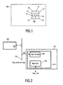
- FIG. 2 illustrates a smart card and a typical prior art terminal. Shown are the smart card (100) and the terminal (101) that communicates via a physical smart card interface (115).
- the terminal (101) comprises a main processor (105) and a generalized standard smart card interface (106) preferably integrated into or embedded in an integrated circuit (IC) (110) in the terminal (101).
- the terminal (101) also comprises a communications/IP link e.g. useful for various e-commerce applications and/or other functions.
- a smart card (100) When inserted in a private and/or home terminal/sub-terminal (101) (both forth denoted terminal), a smart card (100) would be supplied with power from a power supply from a central source, and the ground would be the central ground of the terminal's (101) electrical systems, since a smart card (100) does not have a power supply.
- Control signals of the physical smart card interface (115) in the terminal (101) would typically be provided by a serial smart card interface (106) programmed by the central processor (s) (105) of the terminal (101) to execute the standard protocols to address the smart card's physical interface (115). This is a very cheap and flexible arrangement, which allows developers of terminal/STB software to use standard electronic interfaces and processes to access the cards.
- Figure 3 illustrates an example of an un-tampered circuit according to the present invention. Shown are a smart card/secure access card (100) and a terminal (101) modified according to the present invention.
- the smart card (100) and the physical interface (115) correspond to the ones shown and explained in connection with Figure 2.
- the terminal (101) corresponds to the one shown and explained in connection Figure 2 with the exceptions that it comprises a specialized smart card interface/controller (113) instead of the generalized interface (106 in Figure 2) and that it further comprises a monitoring/detection circuit (114), preferably integrated in/embedded into an IC (110), constituting the functionality of the terminal (101), and connected to the main processor (105) and the physical smart card interface (115).
- Interface pins or other connections of the IC (110) is then directly coupled to the mechanical interface (115) that couples to the smart card (100).
- the IC (110) may be equipped with additional functionality allowing for electrical measurements of the physical/mechanical interface (115) to be made in order to detect tampering with the interface (115) which could allow for spying on the communication via the interface (115).
- the terminal (101) comprises a monitoring process done by the monitoring/detection circuit (114) that monitors and compares certain electrical characteristics of the physical interface (115), as explained in greater detail in the following.
- a smart card (100) is an electrical circuit without internal power source (s) where a terminal (101) supplies the energy, i.e. the currents in the smart card (100).
- Such tampering may e.g. be a monitoring/spy circuit, an extender, etc. with powered sensors/amplifiers.
- the monitoring/detection circuit (114) is able to sense either the AC or DC loss of current to return paths, i.e. sources, other than the terminal itself.
- the monitoring/detection circuit (114) more specifically comprises a first current monitor (102a) coupled to a VDD connection (e. g. the power pin (10) in Figure 1) and measuring/monitoring the current (denoted IDD) and a second current monitor (102b) coupled to a VSS connection (e. g. the ground pin (11) in Figure 1) and measuring/monitoring the current (denoted I ss ).
- the first and second current monitors (102a, 102b) are both connected to a comparator circuit (103) that compares IDD and Iss in order to determine if they are (substantially) equal or different (at all or by a factor greater than a predetermined factor), i. e.
- I ss I DD or not. If they are equal, it signifies that that the current introduced to the smart card (100) from the terminal (100) is also returned again signifying that no tampering circuit has been inserted. If the currents are different (e.g. by more than a margin taking into account normal interference), it signifies that a spy circuit, tampering circuit, extending arrangement, etc. has been inserted.
- the comparator (103) is connected to a controller (104) that on the basis of the signal received from the comparator (103) generates a control signal that is supplied to the main processor (s) (105).
- the main processor (s) (105) may initiate appropriate action (s) if a tampering circuit is detected.
- a tampering circuit In the shown example, no tampering circuit is inserted and therefore the current introduced (Iss) into the card is (substantially) equal to the current (I DD ) returned back to the terminal (100).
- the detection circuit (110) may e. g. be a standard current mirror circuit comparing Iss and I DD using a window function determined by the controller (104) and executed by the comparator (103).
- the capability to re-calibrate the interface between the card (100) and the terminal (101) is not available in the terminal (101). At least not without, the use of special equipment only available at the manufacturing site.
- An alternative embodiment comprises calibration of the interface used to create viable, but non-stable electrical properties at the physical level, e.g. time/timing, voltage and/or current, of the interface to the smart card (100). These properties should be viable enough to allow normal transaction with the card, but so dedicated to the electrical conditions that an insertion of circuit extending arrangement (111,112), e.g. an extender, monitoring device, etc., would cause the interface to fail. The failure of the interface would thus resist the attack of tampering directly.
- a circuit extending arrangement e.g. an extender, monitoring device, etc.
- One implementation of this is to use an impedance-based method that uses current and/or voltage characteristics of the interface to create electrical conditions that are fragile. This is e.g. possible by creating driver circuits in the terminal (101) that are programmable to the electrical impedance of the signal path. Specifically these could use the signal path reflection characteristics. One condition for this may e.g. be that the signal transition time of the driver and a significant proportion of the flight time from source to receiver. In this case, the signal path has the properties of a transmission line thereby making an impedance-based method very practical.
- Yet a further embodiment comprises a monitoring process that compares known electrical characteristics of the interface (as calibrated during manufacture) and the present conditions.
- the monitoring process would regulate the use of the smart card. If the present condition (s) of the actual card inserted into the terminal deviated from the calibrated conditions (e.g. at all and/or within a predetermined margin) then the terminal could e.g. either warn the user and/or the card issuing authority (e.g. using the communications/IP link).
- the transaction, the access, etc. relating to the card would then be terminated and/or carefully monitored by the execution/issuing authority.
- FIG 4 illustrates an example of a tampered circuit according to the present invention. Shown is the arrangement shown in Figure 3 but with an extender (111) inserted and coupled to a spy/monitoring circuit (112). As the inserted extender (111) and/or spy circuit (112) introduces a 'leakage' of current, then I ss will be different from I DD , i.e. all the current supplied by the terminal is not received back, which will be detected by the comparator (103) and signaled by the controller (104) to the main processor (105). In this way, attempts at spying, tampering, etc. is readily detected by simple means.
Landscapes
- Engineering & Computer Science (AREA)
- Physics & Mathematics (AREA)
- General Physics & Mathematics (AREA)
- Theoretical Computer Science (AREA)
- Artificial Intelligence (AREA)
- Computer Vision & Pattern Recognition (AREA)
- Telephone Function (AREA)
- Storage Device Security (AREA)
- Credit Cards Or The Like (AREA)
- Electrotherapy Devices (AREA)
- Lock And Its Accessories (AREA)
Abstract
Description
- The invention relates to a method, and a corresponding terminal, of detecting a presence of a circuit extending/tampering arrangement.
- Smart cards are commonly used in a wide range of applications for the purpose of authority check, payment, satellite TV, data storage, etc. As an example the health insurance and banking industries use smart cards extensively. A smart card usually resembles a credit card in size and shape, but typically contains an embedded microprocessor inside. A terminal with a card reader communicates with the microprocessor which controls access to the data on the card. Smart cards may e.g. be used with a smart card reader attached to or located in a personal computer to authenticate a user, etc. Smart card readers can also be found in mobile phones for SIM reading and vending machines.
- For a private and/or in-home terminal with a smart card reading capability, such as a set top box (STB), integrated digital television (IDTV), Digital TVs, home gateways, access systems, GSMs, Internet audio sets, car systems, etc. the possibilities to spy on the electronic communication between a smart card and/or a secure access card and the terminal is much greater than in a public automated teller machine (ATM) or similar semi-public/public terminals e.g. used for/in connection with e-commerce. This enables attack on the smart card that is not possible with conventional smart card applications in public and/or semi-public terminals, due to the operation in a private sphere.
- A financial and service industry consortium Finread in Europe is attempting to standardize a form of e-commerce terminals used in public ATM and personal computers (PCs), and also for future STBs, IDTV and similar home terminals. Up until now, the consortium has focused on expensive tamper detection and tamper resistant constructions for home e-commerce terminals. Embedded Finread is a part of the Finread consortium examining the issues of low-cost terminals for e-commerce such as IDTV, Jave terminals and STBs. The cost of temper resistant and other counter measures normally adopted for dedicated terminals (i.e. ATMs) are considered to complex and/or expensive for the low cost home terminals.
- A variety of smart cards/secure access cards exist, some with no sophisticated processing power, typically memory only cards. Other cards, typically so-called multi-application/multi-function cards, comprise more advanced properties and functions typically providing secure authentication of the user/owner of the card e.g. in relation to gaining access to equipment, accounts, functions, transfer of money, e-commerce applications, etc.
- Such cards have on-card dynamic data processing capabilities and allocate card memory into independent sections assigned to a specific function and/or application.
- The multi-application/multi-function smart card is distributed by one issuer but allows two or more applications/functions to be resident on the smart card. Typically, advanced 32-bit processor cards are used for this purpose.
- A Java smart card is a smart card with a Java Virtual Machine (JVM) that allows applications to enter and reside on the card. In this way, a Java smart card is a first step towards multi-application smart cards.
- As mentioned traditional smart cards only run one process, while a Java smart card have the capability to run multiple processes on the card, which is an enhancement of the smart card protection capability that allows the smart card not only to perform secured transaction, but also to monitor itself and the presence of an attack.
- A device typically designated a sub-terminal is a device which includes some features of a terminal, i.e. user input, display, storage and a remote connection to the Internet, or a broadcast channel, but not all. Thus a terminal is complete, and examples are e.g. IDTV, STB or GSM (or similar cellular systems like 3G, UMTS, GPRS, etc.), but a sub-terminal is incomplete. In this way, a sub-terminal is a low-cost version of a terminal that provides some but not all the functionality of a terminal. One example of a sub-terminal is e.g. a TV remote control. The sub-terminal may e.g. also be the conditional access module (typically denoted POD (point of deployment) in the US) of the conditional access system implemented in a STB and/or a TV. The conditional access module is a DVB based term derived from the Common Interface concept for DVB terminals.
- Most system can be attacked successfully by a sufficiently resourced attacking entity. It is however necessary to provide sufficient defense (protection and/or detection) against a reasonably resourced security attack or at least provide counter measures that are sufficient to make a single form of attack no more successfully than others. It is also desirable to enable this in an inexpensive way.
- A fake terminal can be used to gain access to an unwary user's pin-code or other application information of the card, which is hard to defend against, and would require other protection detection schemes than provided by the present invention.
- However, a typical security attack on genuine terminals/sub-terminals is the insertion of circuit extending equipment like an extender, sampling circuit (s), emulation circuit (s), etc. in the electrical signal path (s) between a terminal and a smart card, where the circuit extending equipment is coupled both to the smart card to be observed and to any electrical equipment which is used to spy on the communication between the card and the terminal.
- FR 2 659 770 A1 represents the basis for the preambles of claims 1 and 5. It discloses a detector for identifying fraudulent integrated-circuit cards, which have been inserted into a card reader comprising a connector complementary with the connector of the card. The detector comprises: means for disconnecting the connector of the reader of the normal reading circuits and for affording a connection to a monitoring circuit; means in the monitoring circuit for applying specified voltages between specified terminals of the connector; means for measuring voltages and currents between other specified terminals of the connector; means for storing values of voltage and of current corresponding to predetermined configurations of the first and second terminals and voltages applied in respect of non-fraudulent circuits; and means for comparing the stored data with the measured data.
- It is an object of the invention to provide a method (and corresponding terminal) of detecting a presence of a circuit extending/tampering arrangement, where the method (and system) provides detection and/or protection against inserted fraud equipment.
- A further object is to provide this in an inexpensive way. Yet a further object is to enable this using a minimum of electrical measurements.
- This is achieved by a method of detecting a presence of a circuit extending arrangement inserted between a physical interface, connected to a terminal, and a smart card, the physical interface being adapted to receive the smart card), the method comprising the steps of:
- measuring a first current provided from said terminal to said smart card via said physical interface, and
- measuring a second current returned from said smart card to said terminal, and
- comparing whether said first and said second current is substantially equal, and if not determining that a circuit extending arrangement is present
Hereby, a very simple and reliant way of detecting a circuit extending arrangement is obtained.
In one embodiment, said comparing step is performed by use of a window function.
In yet another embodiment,, said comparing step is performed based on a calibration made during manufacture.
In one embodiment, the physical interface has been calibrated to create at least one viable, but non-stable, electrical property at the physical level, the at least one property allowing normal transaction with said smart card, but causing the interface to fail if an circuit extending arrangement is coupled to said physical interface.
Hereby, the failure of the interface would thus resist the attack of tampering directly.
In one embodiment, the at least one non-stable electrical property relates to current and/or voltage characteristics of said physical interface.
In one embodiment, the method further comprises the step of regulating the use of the smart card on the basis of said step of comparing.
In this way, the terminal could e.g. either warn the user and/or the card issuing authority (e. g. using the communications/IP link). The transaction, the access, etc. relating to the card would then be terminated and/or carefully monitored by the execution/issuing authority.
The present invention also relates to a terminal corresponding to the method according to the present invention.
More specifically, the invention relates to a terminal for detecting a presence of a circuit extending arrangement inserted between a physical interface, connected to said terminal, and a smart card, the physical interface being adapted to receive said smart card, the terminal comprising a monitoring circuit comprising - a first measure circuit measuring a first current provided from said terminal to said smart card via said physical interface, and
- a second measure circuit measuring a second current returned from said smart card to said terminal, and
- a comparator connected to said first and second measure circuit and adapted to compare whether said first and said second current is substantially equal, and if not generating a signal representing that a circuit extending arrangement is present.
- In one embodiment, said comparator is adapted to perform said comparison by use of a window function.
- In yet another embodiment, said comparator is adapted to perform said comparison based on a calibration made during manufacture.
- In one embodiment, the terminal further comprises a comparator for comparing said measured at least one electrical characteristic with, at least one electrical characteristic as calibrated during manufacture.
- In one embodiment, the physical interface has been calibrated to create at least one viable, but non-stable, electrical property at the physical level, the at least one property allowing normal transaction with said smart card, but causing the interface to fail if an circuit extending arrangement is coupled to said physical interface.
- In one embodiment, the at least one non-stable electrical property relates to current and/or voltage characteristics of said physical interface.
- In one embodiment, the terminal further comprises: means for regulating the use of the smart card on the basis of said signal from said comparator.
- Further, the invention also relates to a computer readable medium having stored thereon instructions for causing one or more processing units to execute the method according to the present invention.
-
- Figure 1 schematically illustrates a smart card;
- Figure 2 illustrates a smart card and a prior art terminal;
- Figure 3 illustrates an example of an un-tampered circuit according to the present invention;
- Figure 4 illustrates an example of a tampered circuit according to the present invention.
- Figure 1 schematically illustrates a typical smart card. Shown is a security card/a smart card (100) that is well known in the prior art. Typically the card (100) has the form of standard size credit card, although the form, layout, size, etc. may vary. The card (100) typically comprises embedded memory, a processor/controller and input/output (I/O) used for communication with an appropriate card reader/ (sub-) terminal (not shown) via a number of contacts (100'). The shown contacts (100') (the size of which is exaggerated/enlarged for illustrative purposes) complies with the standard of ISO 7816 part 2 and comprises power supply (10), ground (11), three optional contacts/pins (12,14, 15) that may be used for different functionality dependent on the specific card, a bi-directional input/output pin (13), check (16) and reset (17). All of these signals are provided by a terminal, receiving the card, to the smart card (100), and the terminal is expected to monitor the bi-directional input/output (13) according to the standard protocols in order to observe the response of the smart card (100).
- Such a card (100) may be used to store information like PIN-codes, identification information, personal information, security information, etc.
- Figure 2 illustrates a smart card and a typical prior art terminal. Shown are the smart card (100) and the terminal (101) that communicates via a physical smart card interface (115). The terminal (101) comprises a main processor (105) and a generalized standard smart card interface (106) preferably integrated into or embedded in an integrated circuit (IC) (110) in the terminal (101). Optionally the terminal (101) also comprises a communications/IP link e.g. useful for various e-commerce applications and/or other functions.
- When inserted in a private and/or home terminal/sub-terminal (101) (both forth denoted terminal), a smart card (100) would be supplied with power from a power supply from a central source, and the ground would be the central ground of the terminal's (101) electrical systems, since a smart card (100) does not have a power supply. Control signals of the physical smart card interface (115) in the terminal (101) would typically be provided by a serial smart card interface (106) programmed by the central processor (s) (105) of the terminal (101) to execute the standard protocols to address the smart card's physical interface (115). This is a very cheap and flexible arrangement, which allows developers of terminal/STB software to use standard electronic interfaces and processes to access the cards.
- However, the usage of a standard serial interfaces (106) makes the terminal (101) open to forms of tampering by spying on the communication, as described above.
- Figure 3 illustrates an example of an un-tampered circuit according to the present invention. Shown are a smart card/secure access card (100) and a terminal (101) modified according to the present invention. The smart card (100) and the physical interface (115) correspond to the ones shown and explained in connection with Figure 2.
- The terminal (101) corresponds to the one shown and explained in connection Figure 2 with the exceptions that it comprises a specialized smart card interface/controller (113) instead of the generalized interface (106 in Figure 2) and that it further comprises a monitoring/detection circuit (114), preferably integrated in/embedded into an IC (110), constituting the functionality of the terminal (101), and connected to the main processor (105) and the physical smart card interface (115).
- Interface pins or other connections of the IC (110) is then directly coupled to the mechanical interface (115) that couples to the smart card (100). In this way, the IC (110) may be equipped with additional functionality allowing for electrical measurements of the physical/mechanical interface (115) to be made in order to detect tampering with the interface (115) which could allow for spying on the communication via the interface (115).
- In the shown embodiment, the terminal (101) comprises a monitoring process done by the monitoring/detection circuit (114) that monitors and compares certain electrical characteristics of the physical interface (115), as explained in greater detail in the following.
- As mentioned, a smart card (100) is an electrical circuit without internal power source (s) where a terminal (101) supplies the energy, i.e. the currents in the smart card (100).
- This means that the sum of all DC and AC currents supplied to the card (Isc) must be returned to the source, i. e. the smart card interface/controller (113) in the IC (110) in the terminal (101). If there is a leakage of current (either DC and/or AC) from the source that is not returned back to the source then either interference and/or tampering must be present.
- Such tampering may e.g. be a monitoring/spy circuit, an extender, etc. with powered sensors/amplifiers. The monitoring/detection circuit (114) according to the present invention is able to sense either the AC or DC loss of current to return paths, i.e. sources, other than the terminal itself.
- In the embodiment shown in Figure 3, the monitoring/detection circuit (114) more specifically comprises a first current monitor (102a) coupled to a VDD connection (e. g. the power pin (10) in Figure 1) and measuring/monitoring the current (denoted IDD) and a second current monitor (102b) coupled to a VSS connection (e. g. the ground pin (11) in Figure 1) and measuring/monitoring the current (denoted Iss). The first and second current monitors (102a, 102b) are both connected to a comparator circuit (103) that compares IDD and Iss in order to determine if they are (substantially) equal or different (at all or by a factor greater than a predetermined factor), i. e. if Iss (substantially) = IDD or not. If they are equal, it signifies that that the current introduced to the smart card (100) from the terminal (100) is also returned again signifying that no tampering circuit has been inserted. If the currents are different (e.g. by more than a margin taking into account normal interference), it signifies that a spy circuit, tampering circuit, extending arrangement, etc. has been inserted.
- The comparator (103) is connected to a controller (104) that on the basis of the signal received from the comparator (103) generates a control signal that is supplied to the main processor (s) (105). In this way, the main processor (s) (105) may initiate appropriate action (s) if a tampering circuit is detected. In the shown example, no tampering circuit is inserted and therefore the current introduced (Iss) into the card is (substantially) equal to the current (IDD) returned back to the terminal (100).
- The detection circuit (110) may e. g. be a standard current mirror circuit comparing Iss and IDD using a window function determined by the controller (104) and executed by the comparator (103).
- Preferably, the capability to re-calibrate the interface between the card (100) and the terminal (101) is not available in the terminal (101). At least not without, the use of special equipment only available at the manufacturing site.
- An alternative embodiment comprises calibration of the interface used to create viable, but non-stable electrical properties at the physical level, e.g. time/timing, voltage and/or current, of the interface to the smart card (100). These properties should be viable enough to allow normal transaction with the card, but so dedicated to the electrical conditions that an insertion of circuit extending arrangement (111,112), e.g. an extender, monitoring device, etc., would cause the interface to fail. The failure of the interface would thus resist the attack of tampering directly.
- One implementation of this is to use an impedance-based method that uses current and/or voltage characteristics of the interface to create electrical conditions that are fragile. This is e.g. possible by creating driver circuits in the terminal (101) that are programmable to the electrical impedance of the signal path. Specifically these could use the signal path reflection characteristics. One condition for this may e.g. be that the signal transition time of the driver and a significant proportion of the flight time from source to receiver. In this case, the signal path has the properties of a transmission line thereby making an impedance-based method very practical.
- Yet a further embodiment comprises a monitoring process that compares known electrical characteristics of the interface (as calibrated during manufacture) and the present conditions. The monitoring process would regulate the use of the smart card. If the present condition (s) of the actual card inserted into the terminal deviated from the calibrated conditions (e.g. at all and/or within a predetermined margin) then the terminal could e.g. either warn the user and/or the card issuing authority (e.g. using the communications/IP link).
- The transaction, the access, etc. relating to the card would then be terminated and/or carefully monitored by the execution/issuing authority.
- Figure 4 illustrates an example of a tampered circuit according to the present invention. Shown is the arrangement shown in Figure 3 but with an extender (111) inserted and coupled to a spy/monitoring circuit (112). As the inserted extender (111) and/or spy circuit (112) introduces a 'leakage' of current, then Iss will be different from IDD, i.e. all the current supplied by the terminal is not received back, which will be detected by the comparator (103) and signaled by the controller (104) to the main processor (105). In this way, attempts at spying, tampering, etc. is readily detected by simple means.
Claims (9)
- A method of detecting a presence of a circuit extending arrangement (111, 112) inserted between a physical interface (115), connected to a terminal (101), and a smart card (100), the physical interface (115) being adapted to receive the smart card (100), the method being characterized by comprising the steps of:- measuring a first current provided from said terminal (101) to said smart card (100) via said physical interface (115), and- measuring a second current returned from said smart card (100) to said terminal (101), and- comparing whether said first and said second current is substantially equal, and if not determining that a circuit extending arrangement (111, 112) is present.
- A method according to claim 1, characterized in that said comparing step is performed by use of a window function.
- A method according to claims 1 - 2, characterized in that said comparing step is performed based on a calibration made during manufacture.
- Method according to claims 1 - 3, characterized in that the method further comprises the step of regulating the use of the smart card (100) on the basis of said step of comparing.
- A terminal (101) for detecting a presence of a circuit extending arrangement (111, 112) inserted between a physical interface (115), connected to said terminal (101), and a smart card (100), the physical interface (115) being adapted to receive said smart card (100), the terminal (101) comprising a monitoring circuit (114), the monitoring circuit being characterised by:- a first measure circuit (102a) measuring a first current provided from said terminal (101) to said smart card (100) via said physical interface (115), and- a second measure circuit (102b) measuring a second current returned from said smart card (100) to said terminal (101), and- a comparator (103) connected to said first and second measure circuit (102a, 102b) and adapted to compare whether said first and said second current is substantially equal, and if not generating a signal representing that a circuit extending arrangement (111, 112) is present.
- A terminal according to claim 5, characterized in that said comparator (103) is adapted to perform said comparison by use of a window function.
- A terminal according to claims 5 - 6, characterized in that said comparator (103) is adapted to perform said comparison based on a calibration made during manufacture.
- A terminal according to claims 5-7, characterized in that the terminal (101) further comprises means (106) for regulating the use of the smart card (100) on the basis of said signal from said comparator.
- A computer readable medium having stored thereon instructions for causing one or more processing units to execute the method according to any one of claims 1-4.
Priority Applications (1)
| Application Number | Priority Date | Filing Date | Title |
|---|---|---|---|
| EP03815127A EP1588314B1 (en) | 2003-01-14 | 2003-12-04 | Detection of tampering of a smart card interface |
Applications Claiming Priority (4)
| Application Number | Priority Date | Filing Date | Title |
|---|---|---|---|
| EP03100046 | 2003-01-14 | ||
| EP03100046 | 2003-01-14 | ||
| EP03815127A EP1588314B1 (en) | 2003-01-14 | 2003-12-04 | Detection of tampering of a smart card interface |
| PCT/IB2003/005971 WO2004063970A1 (en) | 2003-01-14 | 2003-12-04 | Detection of tampering of a smart card interface |
Publications (2)
| Publication Number | Publication Date |
|---|---|
| EP1588314A1 EP1588314A1 (en) | 2005-10-26 |
| EP1588314B1 true EP1588314B1 (en) | 2006-11-29 |
Family
ID=32695635
Family Applications (1)
| Application Number | Title | Priority Date | Filing Date |
|---|---|---|---|
| EP03815127A Expired - Lifetime EP1588314B1 (en) | 2003-01-14 | 2003-12-04 | Detection of tampering of a smart card interface |
Country Status (9)
| Country | Link |
|---|---|
| US (1) | US7293709B2 (en) |
| EP (1) | EP1588314B1 (en) |
| JP (1) | JP2006513479A (en) |
| KR (1) | KR20050089880A (en) |
| CN (1) | CN100378742C (en) |
| AT (1) | ATE347146T1 (en) |
| AU (1) | AU2003303703A1 (en) |
| DE (1) | DE60310139T2 (en) |
| WO (1) | WO2004063970A1 (en) |
Families Citing this family (23)
| Publication number | Priority date | Publication date | Assignee | Title |
|---|---|---|---|---|
| US7600166B1 (en) * | 2005-06-28 | 2009-10-06 | David Dunn | Method and system for providing trusted access to a JTAG scan interface in a microprocessor |
| JP4754903B2 (en) * | 2005-08-19 | 2011-08-24 | 富士通株式会社 | Semiconductor device and control method in semiconductor device |
| US8126507B2 (en) | 2006-03-22 | 2012-02-28 | British Telecommunications Public Limited Company | Communications device monitoring |
| US9224146B2 (en) * | 2009-09-30 | 2015-12-29 | The Toronto Dominion Bank | Apparatus and method for point of sale terminal fraud detection |
| BR102012006544B1 (en) * | 2012-03-23 | 2021-01-26 | Tecvan Informática Ltda. | secure device control and monitoring module |
| ES2588996T3 (en) * | 2012-10-18 | 2016-11-08 | Wincor Nixdorf International Gmbh | Device for reading a chip card and procedure for detecting a Skimming module |
| US9298956B2 (en) * | 2013-10-04 | 2016-03-29 | Square, Inc. | Tamper protection mesh in an electronic device |
| US9659178B1 (en) | 2013-10-22 | 2017-05-23 | Square, Inc. | Device blanking |
| US10475034B2 (en) * | 2016-02-12 | 2019-11-12 | Square, Inc. | Physical and logical detections for fraud and tampering |
| KR101891658B1 (en) * | 2016-08-01 | 2018-09-28 | 주식회사 바이텔 | Anti- tamper IC card socket |
| US10251260B1 (en) | 2016-08-29 | 2019-04-02 | Square, Inc. | Circuit board to hold connector pieces for tamper detection circuit |
| US10192076B1 (en) | 2016-08-29 | 2019-01-29 | Square, Inc. | Security housing with recesses for tamper localization |
| US10595400B1 (en) | 2016-09-30 | 2020-03-17 | Square, Inc. | Tamper detection system |
| US20180157871A1 (en) * | 2016-12-01 | 2018-06-07 | Nxp B.V. | Capacitive intrusion detection on smartcard reader |
| US10504096B1 (en) | 2017-04-28 | 2019-12-10 | Square, Inc. | Tamper detection using ITO touch screen traces |
| US10592904B2 (en) * | 2017-06-29 | 2020-03-17 | Ncr Corporation | Card shimmer detection |
| US10255603B1 (en) | 2017-08-31 | 2019-04-09 | Sqaure, Inc. | Processor power supply glitch mitigation |
| WO2019162975A1 (en) * | 2018-02-23 | 2019-08-29 | Globalcom Engineering S.P.A. | Method for detecting the presence of a smart card cloning device in an automatic payment and/or withdrawal terminal and respective automatic payment and/or withdrawal terminal |
| US11182794B1 (en) | 2018-03-29 | 2021-11-23 | Square, Inc. | Detecting unauthorized devices using proximity sensor(s) |
| US11257072B1 (en) | 2018-03-29 | 2022-02-22 | Square, Inc. | Detecting unauthorized devices |
| US10733291B1 (en) | 2018-06-11 | 2020-08-04 | Square, Inc. | Bi-directional communication protocol based device security |
| JP2021018745A (en) * | 2019-07-23 | 2021-02-15 | 日立オムロンターミナルソリューションズ株式会社 | Card reader, method for controlling card reader, and automatic teller machine |
| US10810570B1 (en) * | 2019-09-30 | 2020-10-20 | Square, Inc. | Point of sale device with cradle for mobile computing device |
Family Cites Families (5)
| Publication number | Priority date | Publication date | Assignee | Title |
|---|---|---|---|---|
| JPS6435677A (en) * | 1987-07-30 | 1989-02-06 | Omron Tateisi Electronics Co | Testing device for ic card |
| FR2659770B1 (en) * | 1990-03-14 | 1995-08-11 | Sextant Avionique | CARD DETECTION DEVICE WITH FRAUDULENT INTEGRATED CIRCUIT. |
| GB9307252D0 (en) * | 1993-04-07 | 1993-06-02 | Plessey Telecomm | Method and apparatus for verifying the integrity of a smart card |
| JP2003242452A (en) * | 2002-02-19 | 2003-08-29 | Sankyo Seiki Mfg Co Ltd | Self-diagnosis method for ic card reader |
| US7080789B2 (en) * | 2003-05-09 | 2006-07-25 | Stmicroelectronics, Inc. | Smart card including a JTAG test controller and related methods |
-
2003
- 2003-12-04 CN CNB2003801087093A patent/CN100378742C/en not_active Expired - Fee Related
- 2003-12-04 AT AT03815127T patent/ATE347146T1/en not_active IP Right Cessation
- 2003-12-04 US US10/542,388 patent/US7293709B2/en not_active Expired - Lifetime
- 2003-12-04 WO PCT/IB2003/005971 patent/WO2004063970A1/en active IP Right Grant
- 2003-12-04 KR KR1020057012959A patent/KR20050089880A/en not_active Application Discontinuation
- 2003-12-04 AU AU2003303703A patent/AU2003303703A1/en not_active Abandoned
- 2003-12-04 EP EP03815127A patent/EP1588314B1/en not_active Expired - Lifetime
- 2003-12-04 JP JP2004566185A patent/JP2006513479A/en active Pending
- 2003-12-04 DE DE60310139T patent/DE60310139T2/en not_active Expired - Lifetime
Also Published As
| Publication number | Publication date |
|---|---|
| US7293709B2 (en) | 2007-11-13 |
| CN1739110A (en) | 2006-02-22 |
| KR20050089880A (en) | 2005-09-08 |
| DE60310139D1 (en) | 2007-01-11 |
| DE60310139T2 (en) | 2007-09-27 |
| US20060038011A1 (en) | 2006-02-23 |
| WO2004063970A1 (en) | 2004-07-29 |
| AU2003303703A1 (en) | 2004-08-10 |
| ATE347146T1 (en) | 2006-12-15 |
| EP1588314A1 (en) | 2005-10-26 |
| JP2006513479A (en) | 2006-04-20 |
| CN100378742C (en) | 2008-04-02 |
Similar Documents
| Publication | Publication Date | Title |
|---|---|---|
| EP1588314B1 (en) | Detection of tampering of a smart card interface | |
| US7454318B2 (en) | Method and terminal for detecting fake and/or modified smart card | |
| JP3776401B2 (en) | Multi-mode smart card system and related method | |
| US6910638B2 (en) | Smart card that can be configured for debugging and software development using secondary communication port | |
| WO2002031761A1 (en) | Dual mode smart card and associated methods | |
| US8847607B2 (en) | Device for protecting a connector and a communications wire of a memory card reader | |
| WO2006019989A2 (en) | Reference equipment for testing contactless payment devices | |
| US20110253788A1 (en) | Monitoring current level and current into and out of the icc reader power contacts to detect a parasitic shim | |
| US8985447B2 (en) | Secure payment card interface | |
| US20040234111A1 (en) | Method for verifying a fingerprint | |
| KR20030085236A (en) | Tamper-resistant method and data processing system using the same | |
| US10528928B1 (en) | Scanning system with direct access to memory | |
| US8132721B2 (en) | Device for checking the regularity of the operation of automatic payment terminals | |
| US6970068B1 (en) | Apparatus and associated method for limiting access of information transferred between an electronic security device and a host device | |
| TWI646481B (en) | Pairing authentication method for electronic transaction device | |
| EP1205068B1 (en) | Detection of manipulation of an electronic security device inserted in the port of a host device | |
| EP1486906A1 (en) | Method for changing the behavior of a smart card | |
| KR20080075744A (en) | Contact card reader, control method thereof and tv having the contact card reader |
Legal Events
| Date | Code | Title | Description |
|---|---|---|---|
| PUAI | Public reference made under article 153(3) epc to a published international application that has entered the european phase |
Free format text: ORIGINAL CODE: 0009012 |
|
| 17P | Request for examination filed |
Effective date: 20050816 |
|
| AK | Designated contracting states |
Kind code of ref document: A1 Designated state(s): AT BE BG CH CY CZ DE DK EE ES FI FR GB GR HU IE IT LI LU MC NL PT RO SE SI SK TR |
|
| AX | Request for extension of the european patent |
Extension state: AL LT LV MK |
|
| DAX | Request for extension of the european patent (deleted) | ||
| GRAP | Despatch of communication of intention to grant a patent |
Free format text: ORIGINAL CODE: EPIDOSNIGR1 |
|
| GRAS | Grant fee paid |
Free format text: ORIGINAL CODE: EPIDOSNIGR3 |
|
| GRAA | (expected) grant |
Free format text: ORIGINAL CODE: 0009210 |
|
| AK | Designated contracting states |
Kind code of ref document: B1 Designated state(s): AT BE BG CH CY CZ DE DK EE ES FI FR GB GR HU IE IT LI LU MC NL PT RO SE SI SK TR |
|
| PG25 | Lapsed in a contracting state [announced via postgrant information from national office to epo] |
Ref country code: IT Free format text: LAPSE BECAUSE OF FAILURE TO SUBMIT A TRANSLATION OF THE DESCRIPTION OR TO PAY THE FEE WITHIN THE PRESCRIBED TIME-LIMIT;WARNING: LAPSES OF ITALIAN PATENTS WITH EFFECTIVE DATE BEFORE 2007 MAY HAVE OCCURRED AT ANY TIME BEFORE 2007. THE CORRECT EFFECTIVE DATE MAY BE DIFFERENT FROM THE ONE RECORDED. Effective date: 20061129 Ref country code: CH Free format text: LAPSE BECAUSE OF FAILURE TO SUBMIT A TRANSLATION OF THE DESCRIPTION OR TO PAY THE FEE WITHIN THE PRESCRIBED TIME-LIMIT Effective date: 20061129 Ref country code: SK Free format text: LAPSE BECAUSE OF FAILURE TO SUBMIT A TRANSLATION OF THE DESCRIPTION OR TO PAY THE FEE WITHIN THE PRESCRIBED TIME-LIMIT Effective date: 20061129 Ref country code: RO Free format text: LAPSE BECAUSE OF FAILURE TO SUBMIT A TRANSLATION OF THE DESCRIPTION OR TO PAY THE FEE WITHIN THE PRESCRIBED TIME-LIMIT Effective date: 20061129 Ref country code: FI Free format text: LAPSE BECAUSE OF FAILURE TO SUBMIT A TRANSLATION OF THE DESCRIPTION OR TO PAY THE FEE WITHIN THE PRESCRIBED TIME-LIMIT Effective date: 20061129 Ref country code: CZ Free format text: LAPSE BECAUSE OF FAILURE TO SUBMIT A TRANSLATION OF THE DESCRIPTION OR TO PAY THE FEE WITHIN THE PRESCRIBED TIME-LIMIT Effective date: 20061129 Ref country code: AT Free format text: LAPSE BECAUSE OF FAILURE TO SUBMIT A TRANSLATION OF THE DESCRIPTION OR TO PAY THE FEE WITHIN THE PRESCRIBED TIME-LIMIT Effective date: 20061129 Ref country code: SI Free format text: LAPSE BECAUSE OF FAILURE TO SUBMIT A TRANSLATION OF THE DESCRIPTION OR TO PAY THE FEE WITHIN THE PRESCRIBED TIME-LIMIT Effective date: 20061129 Ref country code: NL Free format text: LAPSE BECAUSE OF FAILURE TO SUBMIT A TRANSLATION OF THE DESCRIPTION OR TO PAY THE FEE WITHIN THE PRESCRIBED TIME-LIMIT Effective date: 20061129 Ref country code: BE Free format text: LAPSE BECAUSE OF FAILURE TO SUBMIT A TRANSLATION OF THE DESCRIPTION OR TO PAY THE FEE WITHIN THE PRESCRIBED TIME-LIMIT Effective date: 20061129 Ref country code: LI Free format text: LAPSE BECAUSE OF FAILURE TO SUBMIT A TRANSLATION OF THE DESCRIPTION OR TO PAY THE FEE WITHIN THE PRESCRIBED TIME-LIMIT Effective date: 20061129 |
|
| REG | Reference to a national code |
Ref country code: GB Ref legal event code: FG4D |
|
| PG25 | Lapsed in a contracting state [announced via postgrant information from national office to epo] |
Ref country code: IE Free format text: LAPSE BECAUSE OF NON-PAYMENT OF DUE FEES Effective date: 20061204 |
|
| REG | Reference to a national code |
Ref country code: CH Ref legal event code: EP |
|
| PG25 | Lapsed in a contracting state [announced via postgrant information from national office to epo] |
Ref country code: MC Free format text: LAPSE BECAUSE OF NON-PAYMENT OF DUE FEES Effective date: 20061231 |
|
| REG | Reference to a national code |
Ref country code: IE Ref legal event code: FG4D |
|
| REF | Corresponds to: |
Ref document number: 60310139 Country of ref document: DE Date of ref document: 20070111 Kind code of ref document: P |
|
| PG25 | Lapsed in a contracting state [announced via postgrant information from national office to epo] |
Ref country code: SE Free format text: LAPSE BECAUSE OF FAILURE TO SUBMIT A TRANSLATION OF THE DESCRIPTION OR TO PAY THE FEE WITHIN THE PRESCRIBED TIME-LIMIT Effective date: 20070228 Ref country code: DK Free format text: LAPSE BECAUSE OF FAILURE TO SUBMIT A TRANSLATION OF THE DESCRIPTION OR TO PAY THE FEE WITHIN THE PRESCRIBED TIME-LIMIT Effective date: 20070228 Ref country code: BG Free format text: LAPSE BECAUSE OF FAILURE TO SUBMIT A TRANSLATION OF THE DESCRIPTION OR TO PAY THE FEE WITHIN THE PRESCRIBED TIME-LIMIT Effective date: 20070228 |
|
| PG25 | Lapsed in a contracting state [announced via postgrant information from national office to epo] |
Ref country code: ES Free format text: LAPSE BECAUSE OF FAILURE TO SUBMIT A TRANSLATION OF THE DESCRIPTION OR TO PAY THE FEE WITHIN THE PRESCRIBED TIME-LIMIT Effective date: 20070312 |
|
| PG25 | Lapsed in a contracting state [announced via postgrant information from national office to epo] |
Ref country code: PT Free format text: LAPSE BECAUSE OF FAILURE TO SUBMIT A TRANSLATION OF THE DESCRIPTION OR TO PAY THE FEE WITHIN THE PRESCRIBED TIME-LIMIT Effective date: 20070430 |
|
| NLV1 | Nl: lapsed or annulled due to failure to fulfill the requirements of art. 29p and 29m of the patents act | ||
| REG | Reference to a national code |
Ref country code: CH Ref legal event code: PL |
|
| ET | Fr: translation filed | ||
| PLBE | No opposition filed within time limit |
Free format text: ORIGINAL CODE: 0009261 |
|
| STAA | Information on the status of an ep patent application or granted ep patent |
Free format text: STATUS: NO OPPOSITION FILED WITHIN TIME LIMIT |
|
| 26N | No opposition filed |
Effective date: 20070830 |
|
| PG25 | Lapsed in a contracting state [announced via postgrant information from national office to epo] |
Ref country code: GR Free format text: LAPSE BECAUSE OF FAILURE TO SUBMIT A TRANSLATION OF THE DESCRIPTION OR TO PAY THE FEE WITHIN THE PRESCRIBED TIME-LIMIT Effective date: 20070301 |
|
| PG25 | Lapsed in a contracting state [announced via postgrant information from national office to epo] |
Ref country code: EE Free format text: LAPSE BECAUSE OF FAILURE TO SUBMIT A TRANSLATION OF THE DESCRIPTION OR TO PAY THE FEE WITHIN THE PRESCRIBED TIME-LIMIT Effective date: 20061129 |
|
| PG25 | Lapsed in a contracting state [announced via postgrant information from national office to epo] |
Ref country code: LU Free format text: LAPSE BECAUSE OF NON-PAYMENT OF DUE FEES Effective date: 20061204 Ref country code: HU Free format text: LAPSE BECAUSE OF FAILURE TO SUBMIT A TRANSLATION OF THE DESCRIPTION OR TO PAY THE FEE WITHIN THE PRESCRIBED TIME-LIMIT Effective date: 20070530 Ref country code: TR Free format text: LAPSE BECAUSE OF FAILURE TO SUBMIT A TRANSLATION OF THE DESCRIPTION OR TO PAY THE FEE WITHIN THE PRESCRIBED TIME-LIMIT Effective date: 20061129 |
|
| REG | Reference to a national code |
Ref country code: GB Ref legal event code: 732E |
|
| PG25 | Lapsed in a contracting state [announced via postgrant information from national office to epo] |
Ref country code: CY Free format text: LAPSE BECAUSE OF FAILURE TO SUBMIT A TRANSLATION OF THE DESCRIPTION OR TO PAY THE FEE WITHIN THE PRESCRIBED TIME-LIMIT Effective date: 20061129 |
|
| REG | Reference to a national code |
Ref country code: FR Ref legal event code: TP |
|
| REG | Reference to a national code |
Ref country code: FR Ref legal event code: PLFP Year of fee payment: 13 |
|
| REG | Reference to a national code |
Ref country code: FR Ref legal event code: PLFP Year of fee payment: 14 |
|
| REG | Reference to a national code |
Ref country code: FR Ref legal event code: PLFP Year of fee payment: 15 |
|
| PGFP | Annual fee paid to national office [announced via postgrant information from national office to epo] |
Ref country code: GB Payment date: 20201123 Year of fee payment: 18 Ref country code: FR Payment date: 20201120 Year of fee payment: 18 Ref country code: DE Payment date: 20201119 Year of fee payment: 18 |
|
| REG | Reference to a national code |
Ref country code: DE Ref legal event code: R119 Ref document number: 60310139 Country of ref document: DE |
|
| GBPC | Gb: european patent ceased through non-payment of renewal fee |
Effective date: 20211204 |
|
| PG25 | Lapsed in a contracting state [announced via postgrant information from national office to epo] |
Ref country code: GB Free format text: LAPSE BECAUSE OF NON-PAYMENT OF DUE FEES Effective date: 20211204 Ref country code: DE Free format text: LAPSE BECAUSE OF NON-PAYMENT OF DUE FEES Effective date: 20220701 |
|
| PG25 | Lapsed in a contracting state [announced via postgrant information from national office to epo] |
Ref country code: FR Free format text: LAPSE BECAUSE OF NON-PAYMENT OF DUE FEES Effective date: 20211231 |