EP1587186A2 - Stacked three dimensional photonic crystal, light emitting device, and image display apparatus - Google Patents
Stacked three dimensional photonic crystal, light emitting device, and image display apparatus Download PDFInfo
- Publication number
- EP1587186A2 EP1587186A2 EP05252263A EP05252263A EP1587186A2 EP 1587186 A2 EP1587186 A2 EP 1587186A2 EP 05252263 A EP05252263 A EP 05252263A EP 05252263 A EP05252263 A EP 05252263A EP 1587186 A2 EP1587186 A2 EP 1587186A2
- Authority
- EP
- European Patent Office
- Prior art keywords
- light
- light emitting
- photonic crystal
- stacked
- dimensional photonic
- Prior art date
- Legal status (The legal status is an assumption and is not a legal conclusion. Google has not performed a legal analysis and makes no representation as to the accuracy of the status listed.)
- Granted
Links
Images








Classifications
-
- H—ELECTRICITY
- H01—ELECTRIC ELEMENTS
- H01S—DEVICES USING THE PROCESS OF LIGHT AMPLIFICATION BY STIMULATED EMISSION OF RADIATION [LASER] TO AMPLIFY OR GENERATE LIGHT; DEVICES USING STIMULATED EMISSION OF ELECTROMAGNETIC RADIATION IN WAVE RANGES OTHER THAN OPTICAL
- H01S5/00—Semiconductor lasers
- H01S5/40—Arrangement of two or more semiconductor lasers, not provided for in groups H01S5/02 - H01S5/30
- H01S5/42—Arrays of surface emitting lasers
- H01S5/423—Arrays of surface emitting lasers having a vertical cavity
- H01S5/426—Vertically stacked cavities
-
- H—ELECTRICITY
- H04—ELECTRIC COMMUNICATION TECHNIQUE
- H04N—PICTORIAL COMMUNICATION, e.g. TELEVISION
- H04N9/00—Details of colour television systems
- H04N9/12—Picture reproducers
- H04N9/30—Picture reproducers using solid-state colour display devices
-
- H—ELECTRICITY
- H04—ELECTRIC COMMUNICATION TECHNIQUE
- H04N—PICTORIAL COMMUNICATION, e.g. TELEVISION
- H04N9/00—Details of colour television systems
- H04N9/12—Picture reproducers
- H04N9/31—Projection devices for colour picture display, e.g. using electronic spatial light modulators [ESLM]
- H04N9/3129—Projection devices for colour picture display, e.g. using electronic spatial light modulators [ESLM] scanning a light beam on the display screen
-
- H—ELECTRICITY
- H01—ELECTRIC ELEMENTS
- H01S—DEVICES USING THE PROCESS OF LIGHT AMPLIFICATION BY STIMULATED EMISSION OF RADIATION [LASER] TO AMPLIFY OR GENERATE LIGHT; DEVICES USING STIMULATED EMISSION OF ELECTROMAGNETIC RADIATION IN WAVE RANGES OTHER THAN OPTICAL
- H01S5/00—Semiconductor lasers
- H01S5/10—Construction or shape of the optical resonator, e.g. extended or external cavity, coupled cavities, bent-guide, varying width, thickness or composition of the active region
- H01S5/11—Comprising a photonic bandgap structure
-
- H—ELECTRICITY
- H01—ELECTRIC ELEMENTS
- H01S—DEVICES USING THE PROCESS OF LIGHT AMPLIFICATION BY STIMULATED EMISSION OF RADIATION [LASER] TO AMPLIFY OR GENERATE LIGHT; DEVICES USING STIMULATED EMISSION OF ELECTROMAGNETIC RADIATION IN WAVE RANGES OTHER THAN OPTICAL
- H01S5/00—Semiconductor lasers
- H01S5/10—Construction or shape of the optical resonator, e.g. extended or external cavity, coupled cavities, bent-guide, varying width, thickness or composition of the active region
- H01S5/18—Surface-emitting [SE] lasers, e.g. having both horizontal and vertical cavities
- H01S5/183—Surface-emitting [SE] lasers, e.g. having both horizontal and vertical cavities having only vertical cavities, e.g. vertical cavity surface-emitting lasers [VCSEL]
- H01S5/18397—Plurality of active layers vertically stacked in a cavity for multi-wavelength emission
-
- H—ELECTRICITY
- H01—ELECTRIC ELEMENTS
- H01S—DEVICES USING THE PROCESS OF LIGHT AMPLIFICATION BY STIMULATED EMISSION OF RADIATION [LASER] TO AMPLIFY OR GENERATE LIGHT; DEVICES USING STIMULATED EMISSION OF ELECTROMAGNETIC RADIATION IN WAVE RANGES OTHER THAN OPTICAL
- H01S5/00—Semiconductor lasers
- H01S5/30—Structure or shape of the active region; Materials used for the active region
- H01S5/305—Structure or shape of the active region; Materials used for the active region characterised by the doping materials used in the laser structure
- H01S5/3086—Structure or shape of the active region; Materials used for the active region characterised by the doping materials used in the laser structure doping of the active layer
-
- H—ELECTRICITY
- H01—ELECTRIC ELEMENTS
- H01S—DEVICES USING THE PROCESS OF LIGHT AMPLIFICATION BY STIMULATED EMISSION OF RADIATION [LASER] TO AMPLIFY OR GENERATE LIGHT; DEVICES USING STIMULATED EMISSION OF ELECTROMAGNETIC RADIATION IN WAVE RANGES OTHER THAN OPTICAL
- H01S5/00—Semiconductor lasers
- H01S5/30—Structure or shape of the active region; Materials used for the active region
- H01S5/32—Structure or shape of the active region; Materials used for the active region comprising PN junctions, e.g. hetero- or double- heterostructures
- H01S5/327—Structure or shape of the active region; Materials used for the active region comprising PN junctions, e.g. hetero- or double- heterostructures in AIIBVI compounds, e.g. ZnCdSe-laser
-
- H—ELECTRICITY
- H01—ELECTRIC ELEMENTS
- H01S—DEVICES USING THE PROCESS OF LIGHT AMPLIFICATION BY STIMULATED EMISSION OF RADIATION [LASER] TO AMPLIFY OR GENERATE LIGHT; DEVICES USING STIMULATED EMISSION OF ELECTROMAGNETIC RADIATION IN WAVE RANGES OTHER THAN OPTICAL
- H01S5/00—Semiconductor lasers
- H01S5/30—Structure or shape of the active region; Materials used for the active region
- H01S5/36—Structure or shape of the active region; Materials used for the active region comprising organic materials
-
- H—ELECTRICITY
- H01—ELECTRIC ELEMENTS
- H01S—DEVICES USING THE PROCESS OF LIGHT AMPLIFICATION BY STIMULATED EMISSION OF RADIATION [LASER] TO AMPLIFY OR GENERATE LIGHT; DEVICES USING STIMULATED EMISSION OF ELECTROMAGNETIC RADIATION IN WAVE RANGES OTHER THAN OPTICAL
- H01S5/00—Semiconductor lasers
- H01S5/40—Arrangement of two or more semiconductor lasers, not provided for in groups H01S5/02 - H01S5/30
- H01S5/4025—Array arrangements, e.g. constituted by discrete laser diodes or laser bar
- H01S5/4087—Array arrangements, e.g. constituted by discrete laser diodes or laser bar emitting more than one wavelength
- H01S5/4093—Red, green and blue [RGB] generated directly by laser action or by a combination of laser action with nonlinear frequency conversion
Definitions
- Fig. 1 is a schematic view showing a light emission structure for emitting a plurality of light beams having wavelength distributions different from one another.
- the light emission structure for emitting the plurality of light beams having the different wavelength distributions is obtained by stacking a plurality of three-dimensional photonic crystals (a first photonic crystal 1, a second photonic crystal 2, and a third photonic crystal 3) having photonic band gaps different from one another in a light emitting direction.
- the photonic crystals 1, 2, and 3 include a first resonator structure 7, a second resonator structure 8, and a third resonator structure 9, respectively, each of which serves as a light emitting region.
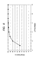
- Fig. 6 is a graph showing a relationship between a period of a three-dimensional photonic crystal and reflectance in a photonic band gap.
- the horizontal axis indicates a period of the crystal as a unit.
- a three-dimensional lattice structure (such as a face centered cubic structure or a diamond opal structure) is obtained using silica spheres and polymer spheres. Then, a gap between the spheres is filled with a lattice material such as a dielectric material. Finally, the silica spheres and the polymer spheres are removed.
- a lattice material filling method there are a sol-gel method and a nanoparticle filling method, and the like.
- a method of removing the silica sphere and the polymer sphere there are a dissolving method using a solvent and a removal method with baking.
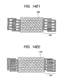
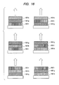
- Fig. 14D1 shows an example in which a dielectric constant is changed by heat energy supplied from the outside to shift the PBG, thereby performing switching.
- a heater 1410 is made in contact with a photonic crystal 1400, heat energy can be supplied thereto to control the PBG based on a change in dielectric constant which is caused by heating.
- means for emitting light corresponding to a absorption wavelength of the photonic crystal or a Peltier element may be used as the heat energy supplying means.
- the stacked light emitting structure of the optical excitation type can be realized using the above-mentioned stacked three-dimensional photonic crystal.
- the example in which only the three photonic crystal layers corresponding to the colors of R, G, and B are stacked is described.
- the number of photonic crystal layers is not limited to three. An arbitrary number of photonic crystal layers can be stacked if necessary. As described above, according to this embodiment, it is possible to realize a light-emitting device for full-color operation.
Landscapes
- Physics & Mathematics (AREA)
- Optics & Photonics (AREA)
- Engineering & Computer Science (AREA)
- Multimedia (AREA)
- Signal Processing (AREA)
- Condensed Matter Physics & Semiconductors (AREA)
- General Physics & Mathematics (AREA)
- Electromagnetism (AREA)
- Optical Modulation, Optical Deflection, Nonlinear Optics, Optical Demodulation, Optical Logic Elements (AREA)
- Optical Integrated Circuits (AREA)
- Liquid Crystal (AREA)
- Lasers (AREA)
Abstract
Description
| Grating structure | Inverse diamond opal structure |
| Constituent Material 1 (refraction index) | TiO2 (n=2.33) |
| Constituent Material 2 (refraction index) | Air or Vacuum (n=1.00) |
| lattice period | a=365 nm |
| Radius of | 0.30a |
| Shape of point defect resonator | Substantial sphere |
| Material of a point defect resonator (refraction index) | TiO2 (n=2.33) |
| Resonator diameter (effective value) | 231.7 nm |
| First photonic crystal | Second photonic crystal | |
| Grating structure | Inverse diamond opal structure | Inverse diamond opal structure |
| High refraction index material (refraction index) | TiO2 (n=2.33) | TiO2 (n=2.33) |
| Low refraction index material (refraction index) | Air or vacuum (n=1.00) | Air or vacuum (n=1.00) |
| Lattice period | a=365 nm | a=432 nm |
| Radius of low refractive index material (air) | 0.30a | 0.30a |
| PBG wavelength | 525 nm to 575 nm | 625 nm to 685 nm |
| First photonic crystal | Second photonic crystal | |
| Shape of a point defect resonator | Substantial sphere | Substantial sphere |
| Material of a point defect resonator (refraction index) | TiO2 (n=2.33) | TiO2 (n=2.33) |
| Resonator diameter (effective value) | 231.7 nm | 274.7 nm |
| Central resonant wavelength | 540 nm | 640 nm |
| First photonic crystal structure | Second photonic crystal structure | Third photonic crystal structure | |
| Grating structure | Inverse diamond opal structure | Inverse diamond opal structure | Inverse diamond opal structure |
| Constituent Material 4 (refraction index) | TiO2 (n=2.33) | TiO2 (n=2.33) | TiO2 (n=2.33) |
| Constituent Material 5 (refraction index) | Air or vacuum vacuum (n=1.00) | Air or vacuum (n=1.00) | Air or vacuum, or (n=1.00) |
| Lattice period | a=300 nm | a=365 nm | a=432 nm |
| Radius of | 0.30a | 0.30a | 0.30a |
| Band gap region | 428 nm to 476 nm | 521 nm to 579 nm | 617 nm to 686 nm |
| First resonator structure | Second resonator structure | Third resonator structure | |
| Shape of defect resonator | Substantial sphere | Substantial sphere | Substantial sphere |
| Material of defect resonator (refraction index) | TiO2 (n=2.33) | TiO2 (n=2.33) | TiO2 (n=2.33) |
| Resonator diameter (effective value) | 190.4 nm | 231.7 nm | 274.7 nm |
| Central resonant wavelength | 443 nm | 540 nm | 640 nm |
| | 1701b | 1701g | 1701r | ||
| Grating structure | Inverse diamond opal | Inverse diamond opal | Inverse diamond opal | ||
| Constituent Material 6 (refraction index) | TiO2 (n=2.33) | TiO2 (n=2.33) | TiO2 (n=2.33) | ||
| Constituent Material 7 (refraction index) | Air (or vacuum) (n=1.00) | Air (or vacuum) (n=1.00) | Air (or vacuum) (n=1.00) | ||
| Dispersion layer radius | 0.30a (a means lattice period.) | 0.30a (a means lattice period.) | 0.30a (a means lattice period.) | ||
| Lattice period (a) | 300 nm | 365 nm | 432 nm | ||
| | 450 nm | 530 nm | 640 nm |
| Stack order | Transmittance | Transmittance | Transmittance |
| B(450nm) | G(530nm) | R(640nm) | |
| (1) Substrate-R-G-B | - | 68.25% | 67.15% |
| (2) Substrate-G-R-B | - | 0.99% | 83.95% |
| (3) Substrate-R-B-G | 2.98% | - | 67.15% |
| (4) Substrate-B-R-G | 0.23% | - | 79.98% |
| (5) Substrate-G-B-R | 7.86% | 0.99% | - |
| (6) Substrate-B-G-R | 0.23% | 1.45% | - |
Claims (13)
- A stacked three-dimensional photonic crystal, which is formed by stacking a plurality of three-dimensional photonic crystals having photonic band gaps different from one another,
characterized in that each of the plurality of three-dimensional photonic crystals includes a resonator in which a point defect is formed. - A stacked three-dimensional photonic crystal according to claim 1, characterized in that the point defect contains an active medium that emits light through excitation.
- A stacked three-dimensional photonic crystal according to claim 1, characterized in that the point defect contains an active medium that emits light through current injection.
- A stacked three-dimensional photonic crystal according to claim 1, characterized in that the point defect contains an active medium that emits light through excitation light irradiation.
- A stacked three-dimensional photonic crystal according to any one of claims 1 to 4, characterized in that:the resonators of the plurality of three-dimensional photonic crystals emit light beams having wavelengths different from one another in a stack direction; andthe plurality of three-dimensional photonic crystals are stacked to successively shift central wavelengths of the photonic band gaps to a short wavelength side in the stack direction.
- A stacked three-dimensional photonic crystal according to any one of claims 1 to 4, characterized in that:the resonators of the plurality of three-dimensional photonic crystals emit light beams having wavelengths different from one another in a direction reverse to a stack direction; andthe plurality of three-dimensional photonic crystals are stacked to successively shift central wavelengths of the photonic band gaps to a long wavelength side in the stack direction.
- A light emitting device, characterized by comprising:the stacked three-dimensional photonic crystal according to any one of claims 2 to 6; andexcitation means for exciting said active medium.
- A light emitting device according to claim 7, characterized by further comprising switching means for controlling a light emitting state of the light emitting device.
- A light emitting device according to claim 8, characterized in that the switching means controls a drive signal supplied to the excitation means.
- A light emitting device according to claim 8, characterized in that the switching means changes a resonant wavelength of each of the resonators to control the light emitting state of the light emitting device.
- A light emitting device according to claim 8, characterized in that the switching means cuts off an optical path of light emitted from each of the resonators to control the light emitting state of the light emitting device.
- A light emitting device according to any one of claims 7 to 11, characterized in that the light emitting device emits light in a wavelength region corresponding to at least one of colors of R, G, and B.
- An image display apparatus, characterized by comprising a plurality of light emitting devices which are arranged, each of which is the light emitting device according to any one of claims 7 to 12.
Applications Claiming Priority (4)
| Application Number | Priority Date | Filing Date | Title |
|---|---|---|---|
| JP2004116806 | 2004-04-12 | ||
| JP2004116806 | 2004-04-12 | ||
| JP2005102596A JP4642527B2 (en) | 2004-04-12 | 2005-03-31 | LAMINATED 3D PHOTONIC CRYSTAL, LIGHT EMITTING ELEMENT AND IMAGE DISPLAY DEVICE |
| JP2005102596 | 2005-03-31 |
Publications (3)
| Publication Number | Publication Date |
|---|---|
| EP1587186A2 true EP1587186A2 (en) | 2005-10-19 |
| EP1587186A3 EP1587186A3 (en) | 2005-11-30 |
| EP1587186B1 EP1587186B1 (en) | 2008-07-23 |
Family
ID=34940773
Family Applications (1)
| Application Number | Title | Priority Date | Filing Date |
|---|---|---|---|
| EP05252263A Expired - Lifetime EP1587186B1 (en) | 2004-04-12 | 2005-04-11 | Stacked three dimensional photonic crystal, light emitting device, and image display apparatus |
Country Status (4)
| Country | Link |
|---|---|
| US (2) | US7462873B2 (en) |
| EP (1) | EP1587186B1 (en) |
| JP (1) | JP4642527B2 (en) |
| DE (1) | DE602005008302D1 (en) |
Cited By (4)
| Publication number | Priority date | Publication date | Assignee | Title |
|---|---|---|---|---|
| DE102006045702A1 (en) * | 2006-09-27 | 2008-04-03 | Osram Opto Semiconductors Gmbh | Opto-electronic component comprises radiation-emitting layer sequence which emits radiation with spectrum, and wavelength conversion area is provided in path of rays of radiation-emitting layer sequence |
| WO2009042455A3 (en) * | 2007-09-27 | 2009-10-22 | Ostendo Technologies, Inc. | Quantum photonic imagers and mehods of fabrication thereof |
| EP3313587A4 (en) * | 2015-06-24 | 2019-03-13 | John N. Magno | IMPROVED ORGANIC ELECTROLUMINESCENT DIODE FOR BAND EDGE EMITTING WITH LOCALIZED TRANSMITTER |
| WO2024200368A1 (en) * | 2023-03-30 | 2024-10-03 | Ams-Osram International Gmbh | Optoelectronic device |
Families Citing this family (40)
| Publication number | Priority date | Publication date | Assignee | Title |
|---|---|---|---|---|
| JP4642527B2 (en) * | 2004-04-12 | 2011-03-02 | キヤノン株式会社 | LAMINATED 3D PHOTONIC CRYSTAL, LIGHT EMITTING ELEMENT AND IMAGE DISPLAY DEVICE |
| CN100507634C (en) * | 2004-04-21 | 2009-07-01 | 松下电器产业株式会社 | Photonic crystal device |
| JP4603847B2 (en) * | 2004-10-15 | 2010-12-22 | キヤノン株式会社 | Resonator, light emitting element, and wavelength conversion element |
| TWI279595B (en) * | 2005-11-14 | 2007-04-21 | Ind Tech Res Inst | Electromagnetic polarizing structure and polarized electromagnetic device |
| US8228604B2 (en) * | 2005-11-14 | 2012-07-24 | Industrial Technology Research Institute | Electromagnetic (EM) wave polarizing structure and method for providing polarized electromagnetic (EM) wave |
| JP2007242945A (en) * | 2006-03-09 | 2007-09-20 | Furukawa Electric Co Ltd:The | Surface emitting semiconductor laser device |
| US20110190167A1 (en) * | 2006-03-22 | 2011-08-04 | Hillis W Daniel | Electromagnetically responsive element with self resonant bodies |
| US8369659B2 (en) | 2006-03-22 | 2013-02-05 | The Invention Science Fund I Llc | High-Q resonators assembly |
| US20070223866A1 (en) * | 2006-03-22 | 2007-09-27 | Searete Llc, A Limited Liability Corporation Of The State Of Delaware | Controllable electromagnetically responsive assembly of self resonant bodies |
| KR100736623B1 (en) * | 2006-05-08 | 2007-07-09 | 엘지전자 주식회사 | Vertical light emitting device and manufacturing method |
| US8941299B2 (en) * | 2006-05-21 | 2015-01-27 | Massachusetts Institute Of Technology | Light emitting device including semiconductor nanocrystals |
| US7674573B2 (en) * | 2006-08-08 | 2010-03-09 | Canon Kabushiki Kaisha | Method for manufacturing layered periodic structures |
| DE102006051745B4 (en) * | 2006-09-28 | 2024-02-08 | OSRAM Opto Semiconductors Gesellschaft mit beschränkter Haftung | LED semiconductor body and use of an LED semiconductor body |
| US7532384B2 (en) * | 2006-11-15 | 2009-05-12 | Massachusetts Institute Of Technology | π-Phase shift device for light |
| US8569696B2 (en) * | 2007-01-30 | 2013-10-29 | Raytheon Company | Imaging system and method using a photonic band gap array |
| DE102007011637A1 (en) * | 2007-03-09 | 2008-09-18 | Ivoclar Vivadent Ag | Light emitting device |
| JP2010050126A (en) * | 2008-08-19 | 2010-03-04 | Central Glass Co Ltd | Ase light source |
| US8264637B2 (en) * | 2008-10-10 | 2012-09-11 | Samsung Electronics Co., Ltd. | Photonic crystal optical filter, reflective color filter, display apparatus using the reflective color filter, and method of manufacturing the reflective color filter |
| US8363185B2 (en) * | 2008-10-10 | 2013-01-29 | Samsung Electronics Co., Ltd. | Photonic crystal optical filter, transmissive color filter, transflective color filter, and display apparatus using the color filters |
| RU2383040C1 (en) * | 2008-10-13 | 2010-02-27 | Государственное образовательное учреждение высшего профессионального образования "Северо-Кавказский государственный технический университет" | Method of making luminescent photonic crystals with controlled radiation directivity |
| GB2468323A (en) * | 2009-03-04 | 2010-09-08 | Dyson Technology Ltd | Fan assembly |
| DE102009030549A1 (en) * | 2009-06-25 | 2010-12-30 | Osram Opto Semiconductors Gmbh | Optical projection device |
| KR101678672B1 (en) * | 2010-08-19 | 2016-11-23 | 삼성전자주식회사 | Display apparatus switchable between reflective mode and transmissive mode |
| CN103650129A (en) * | 2011-05-19 | 2014-03-19 | 港大科桥有限公司 | Chip stacking |
| KR20130115901A (en) * | 2012-04-13 | 2013-10-22 | 삼성디스플레이 주식회사 | Dual mode display device |
| GB201215344D0 (en) * | 2012-08-29 | 2012-10-10 | Ibm | Light-reflecting grating structure for photvoltaic devices |
| US10142034B2 (en) | 2013-09-02 | 2018-11-27 | Philips Lighting Holding B.V. | Optically transmissive electronic device having an optically transmissive light emitting device to transmit optical signal to a second optically transmissive light receiving device through a first optically transmissive light receiving device |
| JP2017509933A (en) * | 2014-03-28 | 2017-04-06 | 華為技術有限公司Huawei Technologies Co.,Ltd. | Optical interconnector, optoelectronic chip system, and optical signal sharing method |
| EP3188260B1 (en) * | 2015-12-31 | 2020-02-12 | Dow Global Technologies Llc | Nanostructure material structures and methods |
| JP6795853B2 (en) * | 2016-02-29 | 2020-12-02 | 国立大学法人京都大学 | Thermal radiant light source |
| CN107390421B (en) * | 2017-08-01 | 2020-11-27 | 京东方科技集团股份有限公司 | A display device and control method thereof |
| US11527519B2 (en) | 2017-11-27 | 2022-12-13 | Seoul Viosys Co., Ltd. | LED unit for display and display apparatus having the same |
| US11282981B2 (en) | 2017-11-27 | 2022-03-22 | Seoul Viosys Co., Ltd. | Passivation covered light emitting unit stack |
| US10892296B2 (en) * | 2017-11-27 | 2021-01-12 | Seoul Viosys Co., Ltd. | Light emitting device having commonly connected LED sub-units |
| US10892297B2 (en) | 2017-11-27 | 2021-01-12 | Seoul Viosys Co., Ltd. | Light emitting diode (LED) stack for a display |
| KR102518369B1 (en) | 2017-12-19 | 2023-04-05 | 삼성전자주식회사 | Light emitting device |
| US11552057B2 (en) | 2017-12-20 | 2023-01-10 | Seoul Viosys Co., Ltd. | LED unit for display and display apparatus having the same |
| EP3788655A4 (en) * | 2018-04-30 | 2022-01-26 | Ostendo Technologies, Inc. | QUANTUM PHOTONIC IMAGER INCORPORATING COLOR-ADJUSTABLE SEMICONDUCTOR LIGHT-LUMINESCENT MICROPIXELS |
| US12256595B2 (en) | 2020-09-25 | 2025-03-18 | Red Bank Technologies Llc | Band edge emission enhanced organic light emitting diode-based devices that emit multiple light wavelengths |
| USD1086287S1 (en) * | 2022-10-08 | 2025-07-29 | Aristocrat Technologies Australia Pty Limited | Display assembly for a bank of gaming machines |
Family Cites Families (10)
| Publication number | Priority date | Publication date | Assignee | Title |
|---|---|---|---|---|
| JP3242192B2 (en) | 1993-03-30 | 2001-12-25 | 株式会社日立製作所 | Semiconductor laser device |
| JP3323872B2 (en) * | 1993-09-21 | 2002-09-09 | 株式会社東芝 | Laser element |
| JPH07263752A (en) * | 1994-03-18 | 1995-10-13 | Sony Corp | Semiconductor color light emitting device |
| US5784400A (en) * | 1995-02-28 | 1998-07-21 | Massachusetts Institute Of Technology | Resonant cavities employing two dimensionally periodic dielectric materials |
| JP2003179315A (en) * | 2001-12-12 | 2003-06-27 | Seiko Epson Corp | Optical module and optical communication system |
| JP2004006567A (en) * | 2002-03-26 | 2004-01-08 | Japan Science & Technology Corp | Point defect three-dimensional photonic crystal optical resonator |
| US6829281B2 (en) * | 2002-06-19 | 2004-12-07 | Finisar Corporation | Vertical cavity surface emitting laser using photonic crystals |
| JP4569942B2 (en) * | 2002-09-26 | 2010-10-27 | 三菱電機株式会社 | Optical active device |
| JP2005157336A (en) * | 2003-11-07 | 2005-06-16 | Canon Inc | Method for manufacturing optical element, optical element having three-dimensional laminated structure |
| JP4642527B2 (en) * | 2004-04-12 | 2011-03-02 | キヤノン株式会社 | LAMINATED 3D PHOTONIC CRYSTAL, LIGHT EMITTING ELEMENT AND IMAGE DISPLAY DEVICE |
-
2005
- 2005-03-31 JP JP2005102596A patent/JP4642527B2/en not_active Expired - Fee Related
- 2005-04-07 US US11/100,588 patent/US7462873B2/en not_active Expired - Fee Related
- 2005-04-11 DE DE602005008302T patent/DE602005008302D1/en not_active Expired - Lifetime
- 2005-04-11 EP EP05252263A patent/EP1587186B1/en not_active Expired - Lifetime
-
2008
- 2008-10-31 US US12/262,353 patent/US20090060410A1/en not_active Abandoned
Cited By (21)
| Publication number | Priority date | Publication date | Assignee | Title |
|---|---|---|---|---|
| DE102006045702A1 (en) * | 2006-09-27 | 2008-04-03 | Osram Opto Semiconductors Gmbh | Opto-electronic component comprises radiation-emitting layer sequence which emits radiation with spectrum, and wavelength conversion area is provided in path of rays of radiation-emitting layer sequence |
| WO2009042455A3 (en) * | 2007-09-27 | 2009-10-22 | Ostendo Technologies, Inc. | Quantum photonic imagers and mehods of fabrication thereof |
| US7623560B2 (en) | 2007-09-27 | 2009-11-24 | Ostendo Technologies, Inc. | Quantum photonic imagers and methods of fabrication thereof |
| US7767479B2 (en) | 2007-09-27 | 2010-08-03 | Ostendo Technologies, Inc. | Quantum photonic imagers and methods of fabrication thereof |
| US7829902B2 (en) | 2007-09-27 | 2010-11-09 | Ostendo Technologies, Inc. | Quantum photonic imagers and methods of fabrication thereof |
| US8049231B2 (en) | 2007-09-27 | 2011-11-01 | Ostendo Technologies, Inc. | Quantum photonic imagers and methods of fabrication thereof |
| US8243770B2 (en) | 2007-09-27 | 2012-08-14 | Ostendo Technologies, Inc. | Quantum photonic imagers and methods of fabrication thereof |
| US8567960B2 (en) | 2007-09-27 | 2013-10-29 | Ostendo Technologies, Inc. | Quantum photonic imagers and methods of fabrication thereof |
| KR20150061662A (en) * | 2007-09-27 | 2015-06-04 | 오스텐도 테크놀로지스 인코포레이티드 | Quantum photonic imagers and methods of fabrication thereof |
| KR20150061663A (en) * | 2007-09-27 | 2015-06-04 | 오스텐도 테크놀로지스 인코포레이티드 | Quantum photonic imagers and methods of fabrication thereof |
| KR20150061664A (en) * | 2007-09-27 | 2015-06-04 | 오스텐도 테크놀로지스 인코포레이티드 | Quantum photonic imagers and methods of fabrication thereof |
| EP3057185A1 (en) * | 2007-09-27 | 2016-08-17 | Ostendo Technologies, Inc. | Quantum photonic imagers and methods of fabrication thereof |
| CN101874330B (en) * | 2007-09-27 | 2017-07-28 | 奥斯坦多科技公司 | Quantum photonic imager and method of manufacturing the same |
| CN107257086A (en) * | 2007-09-27 | 2017-10-17 | 奥斯坦多科技公司 | Quantum photonic imager and its manufacture method |
| CN107257085A (en) * | 2007-09-27 | 2017-10-17 | 奥斯坦多科技公司 | Quantum photonic imager and its manufacture method |
| EP3313587A4 (en) * | 2015-06-24 | 2019-03-13 | John N. Magno | IMPROVED ORGANIC ELECTROLUMINESCENT DIODE FOR BAND EDGE EMITTING WITH LOCALIZED TRANSMITTER |
| US11139456B2 (en) | 2015-06-24 | 2021-10-05 | Red Bank Technologies Llc | Band edge emission enhanced organic light emitting diode with a localized emitter |
| US11387434B2 (en) | 2015-06-24 | 2022-07-12 | Red Bank Technologies Llc | Band edge emission enhanced organic light emitting diode with a localized emitter |
| EP4242704A3 (en) * | 2015-06-24 | 2023-11-22 | Red Bank Technologies LLC | Band edge emission enhanced organic light emitting diode with a localized emitter |
| US11895865B2 (en) | 2015-06-24 | 2024-02-06 | Red Bank Technologies Llc | Band edge emission enhanced organic light emitting diode with a localized emitter |
| WO2024200368A1 (en) * | 2023-03-30 | 2024-10-03 | Ams-Osram International Gmbh | Optoelectronic device |
Also Published As
| Publication number | Publication date |
|---|---|
| US7462873B2 (en) | 2008-12-09 |
| DE602005008302D1 (en) | 2008-09-04 |
| EP1587186A3 (en) | 2005-11-30 |
| EP1587186B1 (en) | 2008-07-23 |
| JP4642527B2 (en) | 2011-03-02 |
| JP2005328040A (en) | 2005-11-24 |
| US20050238310A1 (en) | 2005-10-27 |
| US20090060410A1 (en) | 2009-03-05 |
Similar Documents
| Publication | Publication Date | Title |
|---|---|---|
| EP1587186B1 (en) | Stacked three dimensional photonic crystal, light emitting device, and image display apparatus | |
| JP4560348B2 (en) | Three-dimensional photonic crystal and optical element using the same | |
| US6999669B2 (en) | Photonic crystals | |
| US7733936B2 (en) | Surface emitting laser | |
| JP4612844B2 (en) | Three-dimensional periodic structure and functional element having the same | |
| JP5294280B2 (en) | Polarized semiconductor light emitting device | |
| JP5188009B2 (en) | Three-dimensional periodic structure and functional element and light emitting element having the same | |
| US20060291769A1 (en) | Light emitting source incorporating vertical cavity lasers and other MEMS devices within an electro-optical addressing architecture | |
| US20080107145A1 (en) | Structure having photonic crystal and surface-emitting laser using the same | |
| US9890912B2 (en) | Light-emitting apparatus including photoluminescent layer | |
| WO2000038285A1 (en) | Chiral laser apparatus and method | |
| WO2005036246A1 (en) | Organic laser and liquid crystal display illumination | |
| US7120332B1 (en) | Placement of lumiphores within a light emitting resonator in a visual display with electro-optical addressing architecture | |
| US7151629B2 (en) | Three-dimensional photonic crystal and optical device including the same | |
| JP4921038B2 (en) | Resonator and light emitting device using the same | |
| JP2008537789A (en) | Light emitting source with electro-optic addressing structure | |
| US7352926B2 (en) | Visual display with electro-optical addressing architecture | |
| US7113663B1 (en) | Visual display with electro-optical individual pixel addressing architecture | |
| KR20180003164A (en) | Increase band edge emission organic light emitting diode | |
| JP2001244066A (en) | Light emitting device | |
| WO2025188248A1 (en) | Device for color conversion and method for forming the same | |
| JP2008141166A (en) | Structure having photonic crystal and surface emitting laser using the same |
Legal Events
| Date | Code | Title | Description |
|---|---|---|---|
| PUAI | Public reference made under article 153(3) epc to a published international application that has entered the european phase |
Free format text: ORIGINAL CODE: 0009012 |
|
| PUAL | Search report despatched |
Free format text: ORIGINAL CODE: 0009013 |
|
| AK | Designated contracting states |
Kind code of ref document: A2 Designated state(s): AT BE BG CH CY CZ DE DK EE ES FI FR GB GR HU IE IS IT LI LT LU MC NL PL PT RO SE SI SK TR |
|
| AX | Request for extension of the european patent |
Extension state: AL BA HR LV MK YU |
|
| AK | Designated contracting states |
Kind code of ref document: A3 Designated state(s): AT BE BG CH CY CZ DE DK EE ES FI FR GB GR HU IE IS IT LI LT LU MC NL PL PT RO SE SI SK TR |
|
| AX | Request for extension of the european patent |
Extension state: AL BA HR LV MK YU |
|
| 17P | Request for examination filed |
Effective date: 20060530 |
|
| AKX | Designation fees paid |
Designated state(s): DE FR GB |
|
| 17Q | First examination report despatched |
Effective date: 20060801 |
|
| GRAP | Despatch of communication of intention to grant a patent |
Free format text: ORIGINAL CODE: EPIDOSNIGR1 |
|
| GRAS | Grant fee paid |
Free format text: ORIGINAL CODE: EPIDOSNIGR3 |
|
| GRAA | (expected) grant |
Free format text: ORIGINAL CODE: 0009210 |
|
| AK | Designated contracting states |
Kind code of ref document: B1 Designated state(s): DE FR GB |
|
| REG | Reference to a national code |
Ref country code: GB Ref legal event code: FG4D |
|
| REF | Corresponds to: |
Ref document number: 602005008302 Country of ref document: DE Date of ref document: 20080904 Kind code of ref document: P |
|
| PLBE | No opposition filed within time limit |
Free format text: ORIGINAL CODE: 0009261 |
|
| STAA | Information on the status of an ep patent application or granted ep patent |
Free format text: STATUS: NO OPPOSITION FILED WITHIN TIME LIMIT |
|
| 26N | No opposition filed |
Effective date: 20090424 |
|
| PGFP | Annual fee paid to national office [announced via postgrant information from national office to epo] |
Ref country code: GB Payment date: 20140414 Year of fee payment: 10 |
|
| PGFP | Annual fee paid to national office [announced via postgrant information from national office to epo] |
Ref country code: DE Payment date: 20140430 Year of fee payment: 10 Ref country code: FR Payment date: 20140428 Year of fee payment: 10 |
|
| REG | Reference to a national code |
Ref country code: DE Ref legal event code: R119 Ref document number: 602005008302 Country of ref document: DE |
|
| GBPC | Gb: european patent ceased through non-payment of renewal fee |
Effective date: 20150411 |
|
| PG25 | Lapsed in a contracting state [announced via postgrant information from national office to epo] |
Ref country code: DE Free format text: LAPSE BECAUSE OF NON-PAYMENT OF DUE FEES Effective date: 20151103 Ref country code: GB Free format text: LAPSE BECAUSE OF NON-PAYMENT OF DUE FEES Effective date: 20150411 |
|
| REG | Reference to a national code |
Ref country code: FR Ref legal event code: ST Effective date: 20151231 |
|
| PG25 | Lapsed in a contracting state [announced via postgrant information from national office to epo] |
Ref country code: FR Free format text: LAPSE BECAUSE OF NON-PAYMENT OF DUE FEES Effective date: 20150430 |