EP1587136B1 - Steam oxidization apparatus - Google Patents
Steam oxidization apparatus Download PDFInfo
- Publication number
- EP1587136B1 EP1587136B1 EP03768298A EP03768298A EP1587136B1 EP 1587136 B1 EP1587136 B1 EP 1587136B1 EP 03768298 A EP03768298 A EP 03768298A EP 03768298 A EP03768298 A EP 03768298A EP 1587136 B1 EP1587136 B1 EP 1587136B1
- Authority
- EP
- European Patent Office
- Prior art keywords
- steam
- inert gas
- reactor
- gas
- accompanied
- Prior art date
- Legal status (The legal status is an assumption and is not a legal conclusion. Google has not performed a legal analysis and makes no representation as to the accuracy of the status listed.)
- Expired - Lifetime
Links
Images


Classifications
-
- H—ELECTRICITY
- H10—SEMICONDUCTOR DEVICES; ELECTRIC SOLID-STATE DEVICES NOT OTHERWISE PROVIDED FOR
- H10P—GENERIC PROCESSES OR APPARATUS FOR THE MANUFACTURE OR TREATMENT OF DEVICES COVERED BY CLASS H10
- H10P72/00—Handling or holding of wafers, substrates or devices during manufacture or treatment thereof
- H10P72/04—Apparatus for manufacture or treatment
- H10P72/0402—Apparatus for fluid treatment
-
- H—ELECTRICITY
- H10—SEMICONDUCTOR DEVICES; ELECTRIC SOLID-STATE DEVICES NOT OTHERWISE PROVIDED FOR
- H10P—GENERIC PROCESSES OR APPARATUS FOR THE MANUFACTURE OR TREATMENT OF DEVICES COVERED BY CLASS H10
- H10P14/00—Formation of materials, e.g. in the shape of layers or pillars
- H10P14/60—Formation of materials, e.g. in the shape of layers or pillars of insulating materials
- H10P14/63—Formation of materials, e.g. in the shape of layers or pillars of insulating materials characterised by the formation processes
- H10P14/6302—Non-deposition formation processes
- H10P14/6304—Formation by oxidation, e.g. oxidation of the substrate
- H10P14/6306—Formation by oxidation, e.g. oxidation of the substrate of the semiconductor materials
- H10P14/6312—Formation by oxidation, e.g. oxidation of the substrate of the semiconductor materials of Group III-V semiconductors
-
- H—ELECTRICITY
- H10—SEMICONDUCTOR DEVICES; ELECTRIC SOLID-STATE DEVICES NOT OTHERWISE PROVIDED FOR
- H10P—GENERIC PROCESSES OR APPARATUS FOR THE MANUFACTURE OR TREATMENT OF DEVICES COVERED BY CLASS H10
- H10P14/00—Formation of materials, e.g. in the shape of layers or pillars
- H10P14/60—Formation of materials, e.g. in the shape of layers or pillars of insulating materials
- H10P14/69—Inorganic materials
- H10P14/692—Inorganic materials composed of oxides, glassy oxides or oxide-based glasses
- H10P14/6938—Inorganic materials composed of oxides, glassy oxides or oxide-based glasses the material containing at least one metal element, e.g. metal oxides, metal oxynitrides or metal oxycarbides
- H10P14/6939—Inorganic materials composed of oxides, glassy oxides or oxide-based glasses the material containing at least one metal element, e.g. metal oxides, metal oxynitrides or metal oxycarbides characterised by the metal
- H10P14/69391—Inorganic materials composed of oxides, glassy oxides or oxide-based glasses the material containing at least one metal element, e.g. metal oxides, metal oxynitrides or metal oxycarbides characterised by the metal the material containing aluminium, e.g. Al2O3
-
- H—ELECTRICITY
- H10—SEMICONDUCTOR DEVICES; ELECTRIC SOLID-STATE DEVICES NOT OTHERWISE PROVIDED FOR
- H10P—GENERIC PROCESSES OR APPARATUS FOR THE MANUFACTURE OR TREATMENT OF DEVICES COVERED BY CLASS H10
- H10P14/00—Formation of materials, e.g. in the shape of layers or pillars
- H10P14/60—Formation of materials, e.g. in the shape of layers or pillars of insulating materials
- H10P14/63—Formation of materials, e.g. in the shape of layers or pillars of insulating materials characterised by the formation processes
- H10P14/6302—Non-deposition formation processes
- H10P14/6322—Formation by thermal treatments
Definitions
- the present invention relates to a steam oxidation apparatus for treating an object-to-be-oxidized by steam oxidation, and more particularly to a steam oxidation apparatus capable of suppressing condensation of steam in an inert gas which is accompanied by the steam to be supplied to a reactor (referred to as steam-accompanied inert gas, hereinafter) during the steam oxidation.
- a steam oxidation apparatus capable of suppressing condensation of steam in an inert gas which is accompanied by the steam to be supplied to a reactor (referred to as steam-accompanied inert gas, hereinafter) during the steam oxidation.
- Surface-emitting laser element is a semiconductor laser element capable of emitting laser light in the direction vertical to the surface of the substrate.
- a GaAs-base one for example, has ever been developed, which comprises a pair of DBR (diffractive Bragg reflector) resonators formed on a semiconductor substrate such as GaAs, and composed of an AlGaAs/AlGaAs pair differed from each other in the Al composition, and an AlGaAs-base active layer disposed between the pair of DBR reflectors and serves as a light-emitting region.
- DBR diffractive Bragg reflector
- Fig. 4 is a sectional view showing a configuration of the surface-emitting laser element.
- the surface-emitting laser element 10 has, as shown in Fig. 4 and as being sequentially stacked on an n-type GaAs substrate 12, a stacked structure which comprises a lower DBR resonator 14 composed of an n-type semiconductor multi-layered film, an Al 0.3 Ga 0.7 As lower cladding layer 16, an active layer 18, an Al 0 . 3 Ga 0.7 As upper cladding layer 20, an upper DBR resonator 22 composed of a p-type semiconductor multi-layered film, and a p-type GaAs cap layer 24.
- the lower DBR resonator 14 is configured as the semiconductor multi-layered film composed of 30.5 pairs of n-type Al 0 . 3 Ga 0.8 As layers and n-type Al 0 . 3 Ga 0.1 As layers.
- the upper DBR resonator 22 is configured as the semiconductor multi-layered film composed of 25 pairs of p-type Al 0 . 3 Ga 0.8 As layers and p-type Al 0 . 3 Ga 0.1 As layers.
- a compositional layer of the upper DBR resonator 22 closest to the active layer 18 is formed as a p-type AIAs layer 26 in place of the p-type Al 0.9 Ga 0.1 As layer, wherein exclusive of the center circular region thereof, the peripheral AlAs layer is converted into an Al oxidized layer 28 by selective oxidation.
- the Al oxidized layer 28 functions as a high-electric-resistance current confinement region of the oxidation confinement type.
- the center circular region remains intact as the p-type AlAs layer 26, and functions as a current injection region.
- the cap layer 24 and the upper DBR resonator 22 are etched to form a columnar mesa post 30 having a circular section.
- an SiN x film 32 is formed on the upper surface and side faces of the mesa post 30 and on the upper cladding layer 20 on both sides thereof.
- the SiN x film 32 on the upper surface of the mesa post 30 is removed in an annular form so as to allow the n-GaAs cap layer 24 to expose therein.
- An AuZn electrode having an almost same annular form is formed therein as a p-side electrode 34.
- an AuGe/Ni/Au film is formed as an n-side electrode 36.
- a stacked structure is formed on the n-type GaAs substrate 12 by sequentially stacking the lower DBR resonator 14, lower cladding layer 16, active layer 18, upper cladding layer 20, upper DBR resonator 22, and cap layer 24.
- an SiN x film (not shown) is formed on the cap layer 24 by the plasma CVD process, and further thereon, a photoresist film (not shown) is formed.
- a circular pattern is transferred onto the photoresist film by a photolithographic technique to thereby form a circular etching resist mask (not shown), and then using the resist mask, the SiN x film is etched by the reactive ion etching (RIE) process using a CF 4 gas as an etching gas, to thereby form an SiN x mask.
- RIE reactive ion etching
- the cap layer 24 and upper DBR resonator 22 are etched to reach the upper cladding layer 20 by the reactive ion beam etching (RIBE) process using a chlorine gas, to thereby form the columnar mesa post 30.
- RIBE reactive ion beam etching
- the stacked structure including the mesa post 30 is heated in a steam atmosphere to 350°C to 450°C so as to proceed oxidation until a desired diameter of oxidation confinement is obtained.
- the p-type AIAs layer 26 in the upper DBR resonator 22 is oxidized selectively in a region which falls in the outer circumferential area of the mesa post 30, and thereby the Al oxidized layer 28 is formed, while leaving the center region of the mesa post 30 intact as a p-type AlAs layer 26.
- the double-layered mask of SiN x mask and resist mask is completely removed by the RIE process, and an SiN x film 32 is formed again over the entire surface by the plasma CVD process.
- the SiN x film 32 on the upper surface of the mesa post 30 is removed in an annular pattern, and the p-side electrode 34 composed of an AuZn electrode and having an almost same annular pattern is formed. Further being undergone typically through a process of forming the n-side electrode 36 composed of an AuGe/Ni/Au film on the back surface of the n-type GaAs substrate 12, the surface-emitting laser element 10 is completed.
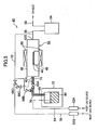
- Fig. 5 is a flow sheet showing a configuration of a conventional steam oxidation apparatus 40.
- the steam oxidation apparatus 40 is an apparatus used for forming the current confinement structure into the surface-emitting laser element by subjecting the high-Al-content layer to steam oxidation, and is equipped with, as shown in Fig. 5 , a single-slice-processing reactor 42 as a reactor for the steam oxidation.
- the reactor 42 comprises a square-tube type quartz chamber 48 for housing a susceptor 46 on which a semiconductor substrate 44 comprising the surface-emitting laser element 10 having the above-described mesa post 30 formed therein is placed, and an electric furnace 50 disposed around the prism-formed quartz chamber 48.
- the electric furnace 50 is a lamp heater, and can elevate temperature of the semiconductor substrate 44 through lamp irradiation.
- the steam oxidation apparatus 40 further comprises a steam-accompanied inert gas system for supplying a steam-accompanied inert gas to the reactor 42, an inert gas system for supplying an inert gas to the reactor 42, a reactor bypass pipe 52 for allowing the steam-accompanied inert gas system and inert gas system to bypass the reactor, and an exhaust system for discharging exhaust gas from the reactor 42.
- the exhaust system has a water-cooled trap 54, and further comprises a fourth gas pipe for introducing gases sent from a gas outlet port 42B of the reactor 42 and from the reactor bypass pipe 52 into the water-cooled trap 54, and a fifth gas pipe 58 for discharging the gas after being passed through the water-cooled trap 54.
- the steam-accompanied inert gas system comprises an H 2 O bubbler 60 which contains pure water, and configured so as to allow the inert gas to blow and bubble therein to thereby make water vapor accompany the inert gas, a first gas pipe 64 connected to an inert gas source and sends the inert gas after being regulated by an MFC (mass flow controller) 62A to the H 2 O bubbler 60 so as to allow it to bubble therein, and a second gas pipe 68 for sending the steam-accompanied inert gas generated in the H 2 O bubbler 60 through an automatic open/close valve 66A to a gas inlet port 42A of the reactor 42.
- MFC mass flow controller
- the inert gas system is connected to the inert gas source, and has a third gas pipe 70 for sending the inert gas after being regulated by the MFC 62B in the flow rate, through the automatic open/close valve 66C to the gas inlet port 42A of the reactor 42.
- the reactor bypass pipe 52 is connected, at one end thereof, to the second gas pipe 68 through the automatic open/close valve 66B and also to the third gas pipe 70 through an automatic open/close valve 66D, and at the other end thereof, to a fourth gas pipe 56 so as to allow the steam-accompanied inert gas and inert gas to bypass the reactor.
- the first to fifth gas pipes are those typically made of 1/4 SUS, and the automatic open/close valves 66A to 66D are disposed closer to the H 2 O bubbler 60 and reactor 42.
- the automatic open/close valves 66A to 66D are electromagnetic diaphragm valves.
- the automatic open/close valve 66A When the steam-accompanied inert gas fed from the steam-accompanied inert gas system is supplied to the reactor 42, the automatic open/close valve 66A is opened, and the automatic open/close valve 66B is closed. When the inert gas fed from the inert gas system is supplied to the reactor 42, the automatic open/close valve 66C is opened and the automatic open/close valve 66D is closed.
- the H 2 O bubbler 60 is housed in the thermostatic oven 72, and water in the H 2 O bubbler 60 is regulated at a predetermined temperature by the thermostatic oven 72.
- a tape-formed heater 74 is wrapped around the second gas pipe 68 between the H 2 O bubbler 60 and reactor 42, so as to heat the second gas pipe 68 to 120°C to 130°C or around, to thereby suppress condensation of the steam in the steam-accompanied inert gas passed through the H 2 O bubbler 60.
- the inert gas in the inert gas system is supplied to the reactor 42, and the semiconductor substrate 44, that is, a stacked structure of the surface-emitting laser element 10 having the mesa post 30 formed therein, is heated to 350°C to 450°C or around using the electric furnace 50.
- the steam-accompanied inert gas is supplied to the reactor 42, and is allowed it to stand for a predetermined duration of time.
- the conventional steam oxidation apparatus 40 configured as described in the above can supply the steam-accompanied inert gas from the steam-accompanied inert gas system to the reactor 42, and can proceed the steam oxidation of the AIAs layer 26 of the surface-emitting laser element 10, while keeping temperature of the surface-emitting laser element 10 having the AIAs layer 26 thereon and the mesa post 30 formed thereon at a predetermined high temperature.
- patent document JP 10144682 A dated 29 May 1998 describes an apparatus for manufacturing a semiconductor device by heat-treating the device using an inert gas.
- the apparatus comprises in particular an H 2 O bubbler equipped with a heater and a quartz tube in which a sample is disposed, the H 2 O bubbler and the quartz tube being connected by a gas pipe.
- Any condensation of a portion of the steam in the steam-accompanied inert gas supplied to the reactor 42, in the oxidation of the high-Al-content layer of the surface-emitting laser element, may vary the amount of steam in the steam-accompanied inert gas and may consequently vary oxidation rate, and this makes it difficult to obtain the current confinement structure in a highly controllable and reproducible manner.
- the present inventors conceived an idea that the second gas pipe 68 between the H 2 O bubbler and reactor 42, automatic open/close valves 66A, 66B and so forth, which cannot readily be heated by a tape-formed heater and are causative of condensation of a part of steam contained in the steam-accompanied inert gas supplied to the reactor 42, will be housed in a thermostatic oven, so as to prevent them from lowering in the temperature and to keep the temperature not lower than the condensation temperature of the steam contained in the steam-accompanied inert gas, to thereby suppress variation in the amount of steam in the steam-accompanied inert gas supplied to the reactor 42, and finally completed the present invention after extensive experiment.
- a steam oxidation apparatus of the present invention proposed based on the above-described findings in order to achieve the above-described object, has a reactor for allowing steam oxidation reaction to proceed, so as to steam-oxidize an object-to-be-oxidized held therein, and is characterized by having:
- the H 2 O bubbler, the second gas pipe between the H 2 O bubbler and the gas inlet port of the reactor, and the first and second automatic open/close valves are housed in a thermostatic oven. This makes it possible to keep these components at a temperature not lower than the condensation temperature of steam in the steam-accompanied inert gas, to thereby suppress condensation of the steam in the steam-accompanied inert gas supplied to the reactor, and to suppress variation in the amount of steam in the steam-accompanied inert gas.
- the third gas pipe in the vicinity of the second automatic open/close valve is preferably housed in the thermostatic oven.
- This also makes it possible to heat the inert gas passing through the third gas pipe in the vicinity of the second automatic open/close valve, and consequently prevents the second automatic open/close valve and second gas pipe from being cooled by the inert gas supplied through the third gas pipe to the reactor, and is successful in obtaining the above-described effects.
- the present invention is preferable enough to obtain the above-described effects if a portion of the gas inlet port side of the reactor is further housed in the thermostatic oven so as to fully heat the second gas pipe in the vicinity of the gas inlet port of the reactor.
- the present invention is preferable enough to obtain the above-described effects if the thermostatic oven is a hot-air-circulating-type thermostatic oven.
- the object-to-be-oxidized is a stacked structural body having a high-Al content layer for fabricating a surface-emitting laser element, wherein the high-Al-content layer is treated by steam oxidation so as to form the oxidation-confinement-type current confinement structure in the surface-emitting laser element.
- the present invention is preferable enough to certainly prevent condensation of the steam in the steam-accompanied inert gas if the inner temperature of the thermostatic oven is set not lower than the condensation temperature of steam in the steam-accompanied inert gas.
- the temperature not higher than the boiling point of the pure water contained in the H 2 O bubbler is successful in preventing boiling of the pure water contained in the H 2 O bubbler.
- This exemplary mode of embodiment is an example of the steam oxidation apparatus of the present invention
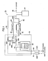
- Fig. 1 is a flow sheet of the steam oxidation apparatus of this exemplary mode of embodiment.
- the steam oxidation apparatus 78 of this exemplary mode of embodiment has the same configuration as that of the conventional steam oxidation apparatus 40, except that it has, in place of the thermostatic oven 72 housing the H 2 O bubbler 60 of the conventional steam oxidation apparatus 40, a thermostatic oven 79 which houses the H 2 O bubbler 60, second gas pipe 68, automatic open/close valves 66A to 66D, a portion of the third gas pipe 70 in the vicinity of the automatic open/close valves 66A to66D, and a portion of the gas inlet port 42A side of the reactor 42, and that the tape-formed heater 74 is not used.
- thermostatic oven 79 a hot-air-circulating-type, constant-temperature thermostatic oven, which is typically thermostatic oven 80 as shown in Fig. 2 , a product of Isuzu Seisakusho Co., Ltd. (trade name: Soyokaze Model ASF-115S), is used.
- a configuration of the thermostatic oven 80 will be explained referring to Fig. 2.
- Fig. 2 is a perspective view showing an appearance of the thermostatic oven 80 of the steam oxidation apparatus 78 according to this exemplary mode of embodiment.
- the thermostatic oven 80 is a hot-air-circulation-type one in which the inner temperature of the oven is adjustable to a predetermined temperature within a range from 30°C to 250°C, and comprises a main unit of the thermostatic oven having a thermostatic chamber isolated and heat-insulated from the external, a temperature control section for regulating temperature of the thermostatic chamber at a predetermined temperature, and a safety device for preventing overheating of the thermostatic chamber.
- the main unit of the thermostatic oven has the thermostatic chamber 82 incorporated therein, and comprises a cabinet 84 kept under heating using a heat-insulating material and opened to the front, and a door 86 disposed on the front plane of the cabinet 84.
- a packing 88 for improving air tightness and heat-insulating property of the thermostatic chamber 82 when the door 86 is closed
- a left-side-panel hole 90 and a right-side-panel hole 92 respectively, for the convenience of introducing the gas pipes and so forth from the external into the thermostatic chamber 82.
- the thermostatic chamber 82 is provided with a plurality of shelf plates 94 on which instruments or the like can be placed.
- the door 86 can be swung leftward or rightward, and has a grip 96 used for opening/closing the door 86, and a double-glassed observation port 98 disposed at the center portion of the door 86.
- the temperature control section comprises an operation panel 100 through which set temperature, set time and so forth are entered, a temperature sensor (not shown) for measuring temperature in the inner space of the thermostatic chamber 82, a heater 102 for heating the inner space of the thermostatic chamber 82 and for keeping the temperature therein at the set temperature, a fan 104 for keeping the inner space of the thermostatic chamber 82 at a uniform temperature by allowing the air to circulate therein, an exhaust damper 106 for maintaining pressure of the inner space of the thermostatic chamber 82 at normal pressure, and a power cord 108 for allowing power supply from a power source.
- the safety device has a safety breaker 110 for disconnecting a power source of the heater 102, and an overheat preventive device 112 with a dial for setting an operating temperature of the safety breaker 110.
- the first gas pipe 64 and third gas pipe 70 are passed through the left-side-panel hole 90 into the thermostatic chamber 82, and the H 2 O bubbler 60 and the automatic open/close valves 66A to 66D are attached typically on the shelf plate 94 or the like.
- the reactor 42 is attached so as to space the electric furnace 50 by 3 cm or around from the right side panel of the thermostatic oven 80, and so that a portion of the gas inlet port 42A side thereof is inserted through the right-side-panel hole 92 into the thermostatic chamber 82. Also the reactor bypass pipe 52 is drawn out from the right-side-panel hole 92.
- the left-side-panel hole 90 is tightly closed except for the portion through which the first gas pipe 64 and third gas pipe 70 are inserted, and the right-side-panel hole 92 is tightly closed except for the portion through which the reactor 42 and reactor bypass pipe 52 are inserted.
- the automatic open/close valves 66A to 66D must be such as those durable to temperatures around 150°C.
- Fig. 3 is an exemplary time table in the process of steam-oxidizing the AlAs layer 26 to thereby form the oxidation-confinement-type current confinement structure into the surface-emitting laser element 10, wherein the abscissa plots time, and the ordinates plots temperature of the semiconductor substrate 44.
- N 2 gas was used as the inert gas.
- flow rate of N 2 gas is adjusted to 4 slm by the MFC 62B, the automatic open/close valve 66D is closed, the automatic open/close valve 66C is opened, and N 2 gas is supplied to the reactor 42.
- flow rate of N 2 gas is adjusted to 4 slm by the MFC 62A, the automatic open/close valve 66A is closed, and the automatic open/close valve 66B is opened.
- Temperature in the thermostatic chamber 82 is then set to a temperature not lower than the condensation temperature of steam in the steam-accompanied inert gas (referred to as steam-accompanied N 2 gas, hereinafter) using N 2 gas as the inert gas after reaching a steady state, and not higher than the boiling point of the pure water housed in the H 2 O bubbler, typically at 90°C, the bubbling is started in the H 2 O bubbler 60, and this state is held until a steady state of the steam-accompanied N 2 gas is reached.
- steam-accompanied N 2 gas the condensation temperature of steam in the steam-accompanied inert gas
- the automatic open/close valve 66C is closed so as to terminate the N 2 gas supply
- the automatic open/close valve 66B is closed
- the automatic open/close valve 66A is opened so as to supply the steam-accompanied N 2 gas to the reactor 42, to thereby replace the inner atmosphere of the reactor 42 with the steam-accompanied N 2 gas.
- the electric furnace 50 is activated.
- temperature of the semiconductor substrate 44 that is the temperature of the stacked structure of the surface-emitting laser element 10 having the mesa post 30 formed therein, reaches 450°C, and this proceeds the steam oxidation of the AlAs layer 26.
- the electric furnace 50 is inactivated, the automatic open/close valve 66B is closed so as to stop supply of the steam-accompanied N 2 gas, the automatic open/close valve 66C is opened so as to send N 2 gas into the reactor 42 and replace the inner atmosphere of the reactor with the N 2 gas, to thereby terminate the steam oxidation.
- the H 2 O bubbler 60, the second gas pipe 68 between the H 2 O bubbler 60 and the gas inlet port 42A of the reactor 42, automatic open/close valves 66A to 66D, a portion of the third gas pipe 70 in the vicinity of the automatic open/close valves 66A to66D, and a portion of the gas inlet port 42A side of the reactor 42 are housed in the thermostatic oven 72, so as to keep these components at a temperature not lower than the condensation temperature of the steam in the steam-accompanied N 2 gas, and this is successful in suppressing condensation of the steam in the steam-accompanied N 2 gas supplied through the H 2 O bubbler 60 to the reactor 42.
- the H 2 O bubbler, the second gas pipe between the H 2 O bubbler and the gas inlet port of the reactor, and the first and second automatic open/close valves are house in the thermostatic oven. This makes it possible to keep these components at a temperature not lower than the condensation temperature of steam contained in the steam-accompanied inert gas, to thereby suppress variation in the amount of steam in the steam-accompanied inert gas supplied to the reactor.
Landscapes
- Semiconductor Lasers (AREA)
- Formation Of Insulating Films (AREA)
Description
- The present invention relates to a steam oxidation apparatus for treating an object-to-be-oxidized by steam oxidation, and more particularly to a steam oxidation apparatus capable of suppressing condensation of steam in an inert gas which is accompanied by the steam to be supplied to a reactor (referred to as steam-accompanied inert gas, hereinafter) during the steam oxidation.
- Surface-emitting laser element is a semiconductor laser element capable of emitting laser light in the direction vertical to the surface of the substrate. As the surface-emitting laser element, a GaAs-base one, for example, has ever been developed, which comprises a pair of DBR (diffractive Bragg reflector) resonators formed on a semiconductor substrate such as GaAs, and composed of an AlGaAs/AlGaAs pair differed from each other in the Al composition, and an AlGaAs-base active layer disposed between the pair of DBR reflectors and serves as a light-emitting region.
- In this type of surface-emitting layer element, it is necessary to restrict a sectional area of current path of current injected into the active layer, for the purpose of raising the emission efficiency and lowering the threshold current. In recent years, as a method of restricting the current path, a method of forming a current confinement structure is becoming a mainstream, in which a high-Al-content layer, typically an AlAs layer, is interlaced in a multi-layered film composing the DBR reflector, and only a portion of the high-Al-content layer is selectively oxidized to thereby convert it into Al2O3 having a large electric resistance.
- An exemplary configuration of a surface-emitting laser element having the current confinement structure obtained by oxidizing an AIAs layer will be explained referring to
Fig. 4. Fig. 4 is a sectional view showing a configuration of the surface-emitting laser element. - The surface-emitting
laser element 10 has, as shown inFig. 4 and as being sequentially stacked on an n-type GaAs substrate 12, a stacked structure which comprises alower DBR resonator 14 composed of an n-type semiconductor multi-layered film, an Al0.3Ga0.7Aslower cladding layer 16, anactive layer 18, an Al0.3Ga0.7Asupper cladding layer 20, anupper DBR resonator 22 composed of a p-type semiconductor multi-layered film, and a p-typeGaAs cap layer 24. - The
lower DBR resonator 14 is configured as the semiconductor multi-layered film composed of 30.5 pairs of n-type Al0.3Ga0.8As layers and n-type Al0.3Ga0.1As layers. - The
upper DBR resonator 22 is configured as the semiconductor multi-layered film composed of 25 pairs of p-type Al0.3Ga0.8As layers and p-type Al0.3Ga0.1As layers. - A compositional layer of the
upper DBR resonator 22 closest to theactive layer 18 is formed as a p-type AIAs layer 26 in place of the p-type Al0.9Ga0.1As layer, wherein exclusive of the center circular region thereof, the peripheral AlAs layer is converted into an Al oxidizedlayer 28 by selective oxidation. - The Al oxidized
layer 28 functions as a high-electric-resistance current confinement region of the oxidation confinement type. On the other hand, the center circular region remains intact as the p-type AlAs layer 26, and functions as a current injection region. - The
cap layer 24 and theupper DBR resonator 22 are etched to form acolumnar mesa post 30 having a circular section. - On the upper surface and side faces of the
mesa post 30 and on theupper cladding layer 20 on both sides thereof, an SiNxfilm 32 is formed. - The SiNx
film 32 on the upper surface of themesa post 30 is removed in an annular form so as to allow the n-GaAs cap layer 24 to expose therein. An AuZn electrode having an almost same annular form is formed therein as a p-side electrode 34. - On the back surface of the n-
type GaAs substrate 12, an AuGe/Ni/Au film is formed as an n-side electrode 36. - In fabrication of the surface-emitting
laser element 10, first a stacked structure is formed on the n-type GaAs substrate 12 by sequentially stacking thelower DBR resonator 14,lower cladding layer 16,active layer 18,upper cladding layer 20,upper DBR resonator 22, andcap layer 24. Next, an SiNx film (not shown) is formed on thecap layer 24 by the plasma CVD process, and further thereon, a photoresist film (not shown) is formed. - Next, a circular pattern is transferred onto the photoresist film by a photolithographic technique to thereby form a circular etching resist mask (not shown), and then using the resist mask, the SiNx film is etched by the reactive ion etching (RIE) process using a CF4 gas as an etching gas, to thereby form an SiNx mask.
- Next, using the double-layered mask of the resist mask and SiNx mask, the
cap layer 24 andupper DBR resonator 22 are etched to reach theupper cladding layer 20 by the reactive ion beam etching (RIBE) process using a chlorine gas, to thereby form thecolumnar mesa post 30. - Next, the stacked structure including the
mesa post 30 is heated in a steam atmosphere to 350°C to 450°C so as to proceed oxidation until a desired diameter of oxidation confinement is obtained. - By this process, the p-
type AIAs layer 26 in theupper DBR resonator 22 is oxidized selectively in a region which falls in the outer circumferential area of themesa post 30, and thereby the Al oxidizedlayer 28 is formed, while leaving the center region of themesa post 30 intact as a p-type AlAs layer 26. - Next, the double-layered mask of SiNx mask and resist mask is completely removed by the RIE process, and an SiNx film 32 is formed again over the entire surface by the plasma CVD process.
- Next, the SiNx
film 32 on the upper surface of themesa post 30 is removed in an annular pattern, and the p-side electrode 34 composed of an AuZn electrode and having an almost same annular pattern is formed. Further being undergone typically through a process of forming the n-side electrode 36 composed of an AuGe/Ni/Au film on the back surface of the n-type GaAs substrate 12, the surface-emittinglaser element 10 is completed. - Conventionally, the above-described steam oxidation of the
AlAs layer 26 has been carried out using a steam oxidation apparatus as explained below. Next paragraphs will describe, referring toFig. 5 , a configuration of a conventional steam oxidation apparatus used for forming the oxidation-confinement-type current confinement structure in the surface-emitting laser element, by oxidizing a high-Al-content layer.Fig. 5 is a flow sheet showing a configuration of a conventionalsteam oxidation apparatus 40. - The
steam oxidation apparatus 40 is an apparatus used for forming the current confinement structure into the surface-emitting laser element by subjecting the high-Al-content layer to steam oxidation, and is equipped with, as shown inFig. 5 , a single-slice-processing reactor 42 as a reactor for the steam oxidation. - The
reactor 42 comprises a square-tubetype quartz chamber 48 for housing asusceptor 46 on which asemiconductor substrate 44 comprising the surface-emittinglaser element 10 having the above-describedmesa post 30 formed therein is placed, and anelectric furnace 50 disposed around the prism-formedquartz chamber 48. - The
electric furnace 50 is a lamp heater, and can elevate temperature of thesemiconductor substrate 44 through lamp irradiation. - The
steam oxidation apparatus 40 further comprises a steam-accompanied inert gas system for supplying a steam-accompanied inert gas to thereactor 42, an inert gas system for supplying an inert gas to thereactor 42, areactor bypass pipe 52 for allowing the steam-accompanied inert gas system and inert gas system to bypass the reactor, and an exhaust system for discharging exhaust gas from thereactor 42. - The exhaust system has a water-cooled
trap 54, and further comprises a fourth gas pipe for introducing gases sent from agas outlet port 42B of thereactor 42 and from thereactor bypass pipe 52 into the water-cooledtrap 54, and afifth gas pipe 58 for discharging the gas after being passed through the water-cooledtrap 54. - The steam-accompanied inert gas system comprises an H2O bubbler 60 which contains pure water, and configured so as to allow the inert gas to blow and bubble therein to thereby make water vapor accompany the inert gas, a
first gas pipe 64 connected to an inert gas source and sends the inert gas after being regulated by an MFC (mass flow controller) 62A to the H2O bubbler 60 so as to allow it to bubble therein, and asecond gas pipe 68 for sending the steam-accompanied inert gas generated in the H2O bubbler 60 through an automatic open/close valve 66A to agas inlet port 42A of thereactor 42. - The inert gas system is connected to the inert gas source, and has a
third gas pipe 70 for sending the inert gas after being regulated by theMFC 62B in the flow rate, through the automatic open/close valve 66C to thegas inlet port 42A of thereactor 42. - The
reactor bypass pipe 52 is connected, at one end thereof, to thesecond gas pipe 68 through the automatic open/close valve 66B and also to thethird gas pipe 70 through an automatic open/close valve 66D, and at the other end thereof, to afourth gas pipe 56 so as to allow the steam-accompanied inert gas and inert gas to bypass the reactor. - The first to fifth gas pipes are those typically made of 1/4 SUS, and the automatic open/
close valves 66A to 66D are disposed closer to the H2O bubbler 60 andreactor 42. - The automatic open/
close valves 66A to 66D are electromagnetic diaphragm valves. - When the steam-accompanied inert gas fed from the steam-accompanied inert gas system is supplied to the
reactor 42, the automatic open/close valve 66A is opened, and the automatic open/close valve 66B is closed. When the inert gas fed from the inert gas system is supplied to thereactor 42, the automatic open/close valve 66C is opened and the automatic open/close valve 66D is closed. - It is possible to send the steam-accompanied inert gas fed from the steam-accompanied inert gas system to the
reactor bypass pipe 52, by closing the automatic open/close valve 66A and opening the automatic open/close valve 66B. It is also possible to send the inert gas fed from the inert gas system to thereactor bypass pipe 52, by closing the automatic open/close valve 66C and by opening the automatic open/close valve 66D. - The H2O
bubbler 60 is housed in thethermostatic oven 72, and water in the H2O bubbler 60 is regulated at a predetermined temperature by thethermostatic oven 72. - A tape-formed
heater 74 is wrapped around thesecond gas pipe 68 between the H2O bubbler 60 andreactor 42, so as to heat thesecond gas pipe 68 to 120°C to 130°C or around, to thereby suppress condensation of the steam in the steam-accompanied inert gas passed through the H2O bubbler 60. - To form the oxidation-confinement-type current confinement structure in the surface-emitting
laser element 10 by oxidizing theAIAs layer 26 using thesteam oxidation apparatus 40, first the inert gas in the inert gas system is supplied to thereactor 42, and thesemiconductor substrate 44, that is, a stacked structure of the surface-emittinglaser element 10 having themesa post 30 formed therein, is heated to 350°C to 450°C or around using theelectric furnace 50. - Next, in place of the inert gas, the steam-accompanied inert gas is supplied to the
reactor 42, and is allowed it to stand for a predetermined duration of time. - The conventional
steam oxidation apparatus 40 configured as described in the above can supply the steam-accompanied inert gas from the steam-accompanied inert gas system to thereactor 42, and can proceed the steam oxidation of theAIAs layer 26 of the surface-emittinglaser element 10, while keeping temperature of the surface-emittinglaser element 10 having theAIAs layer 26 thereon and themesa post 30 formed thereon at a predetermined high temperature. - It is to be noted that patent document
JP 10144682 A dated 29 May 1998 - It is, however, practically difficult to wrap the tape-formed
heater 74 uniformly around the gas pipes in the conventionalsteam oxidation apparatus 40, and non-uniform wrapping of the tape-formedheater 74 possibly occurs, for example, at abent portion 76 of thesecond gas pipe 68 sometimes resulted in only an insufficient heating of that portion. - It has also been difficult to sufficiently heat the automatic open/
close valves heater 74 due to their structures and shapes. In particular, thesecond gas pipe 68 in the vicinity of thegas inlet port 42A of thereactor 42 is difficult to be fully wrapped by the tape-formedheater 74, and this sometimes resulted in only an insufficient heating. - As a consequence, there was a problem in that the path of the steam-accompanied inert gas always had a portion which could not fully be heated, and this resulted in condensation of the steam in the steam-accompanied inert gas in that portion.
- Any condensation of a portion of the steam in the steam-accompanied inert gas supplied to the
reactor 42, in the oxidation of the high-Al-content layer of the surface-emitting laser element, may vary the amount of steam in the steam-accompanied inert gas and may consequently vary oxidation rate, and this makes it difficult to obtain the current confinement structure in a highly controllable and reproducible manner. - Although the forgoing paragraphs described the case where the
AlAs layer 26 of the surface-emittinglaser element 10 was treated by steam oxidation, the same problem will apply also to the steam oxidation apparatus in general in which an object-to-be-oxidized housed in the reactor is treated by steam oxidation. - It is therefore an object of the present invention to provide a steam oxidation apparatus capable of ensuring a desirable controllability and reproducibility of the steam oxidation of an object-to-be-oxidized housed in the reactor, by suppressing condensation of the steam in the steam-accompanied inert gas supplied to the reactor.
- The invention is defined in the appended set of claims.
- To solve the above-described subjects, the present inventors conceived an idea that the
second gas pipe 68 between the H2O bubbler andreactor 42, automatic open/close valves reactor 42, will be housed in a thermostatic oven, so as to prevent them from lowering in the temperature and to keep the temperature not lower than the condensation temperature of the steam contained in the steam-accompanied inert gas, to thereby suppress variation in the amount of steam in the steam-accompanied inert gas supplied to thereactor 42, and finally completed the present invention after extensive experiment. - A steam oxidation apparatus of the present invention, proposed based on the above-described findings in order to achieve the above-described object, has a reactor for allowing steam oxidation reaction to proceed, so as to steam-oxidize an object-to-be-oxidized held therein, and is characterized by having:
- a steam-accompanied inert gas system which comprises an H2O bubbler containing pure water, allowing an inert gas to blow and bubble in the contained pure water to thereby produce a steam-accompanied inert gas in which an inert gas is accompanied by steam; a first gas pipe for allowing the inert gas to blow into the H2O bubbler at a predetermined flow rate; and a second gas pipe for sending the steam-accompanied inert gas through a first automatic open/close valve to a gas inlet port of the reactor; and
- an inert gas system having a third gas pipe for sending the inert gas at a predetermined flow rate through a second automatic open/close valve to a gas inlet port of the reactor;
- wherein the H2O bubbler, the second gas pipe between the H2O bubbler and the gas inlet port of the reactor, and the first and second automatic open/close valves are housed in a thermostatic oven.
- In the steam oxidation apparatus of the present invention, the H2O bubbler, the second gas pipe between the H2O bubbler and the gas inlet port of the reactor, and the first and second automatic open/close valves are housed in a thermostatic oven. This makes it possible to keep these components at a temperature not lower than the condensation temperature of steam in the steam-accompanied inert gas, to thereby suppress condensation of the steam in the steam-accompanied inert gas supplied to the reactor, and to suppress variation in the amount of steam in the steam-accompanied inert gas.
- It is therefore possible to obtain a desirable controllability and reproducibility of steam oxidation of an object-to-be-oxidized held in the reactor, while keeping reaction conditions for the steam oxidation reaction constant.
- In the present invention, further the third gas pipe in the vicinity of the second automatic open/close valve is preferably housed in the thermostatic oven. This successfully prevents the second automatic open/close valve and second gas pipe from being cooled due to heat conduction via the third gas pipe. This also makes it possible to heat the inert gas passing through the third gas pipe in the vicinity of the second automatic open/close valve, and consequently prevents the second automatic open/close valve and second gas pipe from being cooled by the inert gas supplied through the third gas pipe to the reactor, and is successful in obtaining the above-described effects.
- The present invention is preferable enough to obtain the above-described effects if a portion of the gas inlet port side of the reactor is further housed in the thermostatic oven so as to fully heat the second gas pipe in the vicinity of the gas inlet port of the reactor.
- The present invention is preferable enough to obtain the above-described effects if the thermostatic oven is a hot-air-circulating-type thermostatic oven.
- In one preferable embodiment of the present invention, the object-to-be-oxidized is a stacked structural body having a high-Al content layer for fabricating a surface-emitting laser element, wherein the high-Al-content layer is treated by steam oxidation so as to form the oxidation-confinement-type current confinement structure in the surface-emitting laser element.
- This makes it possible to form the oxidation-confinement-type current confinement structure in a highly controllable and reproducible manner.
- The present invention is preferable enough to certainly prevent condensation of the steam in the steam-accompanied inert gas if the inner temperature of the thermostatic oven is set not lower than the condensation temperature of steam in the steam-accompanied inert gas. The temperature not higher than the boiling point of the pure water contained in the H2O bubbler is successful in preventing boiling of the pure water contained in the H2O bubbler.
-
-
Fig. 1 is a flow sheet showing a configuration of a steam oxidation apparatus of one embodiment. -
Fig.2 is a perspective view showing an appearance of a thermostatic oven used for the steam oxidation apparatus of the embodiment. -
Fig. 3 is a time table showing a method of forming a current confinement structure in a surface-emitting laser element by treating an AlAs layer by steam oxidation using the steam oxidation apparatus of the embodiment. -
Fig. 4 is a sectional view showing an exemplary configuration of the surface-emitting laser element. -
Fig. 5 is a flow sheet showing a configuration of a conventional steam oxidation apparatus. - An embodiment of the present invention will specifically be detailed below, referring to exemplary modes of embodiment and attached drawings.
- This exemplary mode of embodiment is an example of the steam oxidation apparatus of the present invention, and
Fig. 1 is a flow sheet of the steam oxidation apparatus of this exemplary mode of embodiment. - As shown in
Fig. 1 , thesteam oxidation apparatus 78 of this exemplary mode of embodiment has the same configuration as that of the conventionalsteam oxidation apparatus 40, except that it has, in place of thethermostatic oven 72 housing the H2O bubbler 60 of the conventionalsteam oxidation apparatus 40, athermostatic oven 79 which houses the H2O bubbler 60,second gas pipe 68, automatic open/close valves 66A to 66D, a portion of thethird gas pipe 70 in the vicinity of the automatic open/close valves 66A to66D, and a portion of thegas inlet port 42A side of thereactor 42, and that the tape-formedheater 74 is not used. - In this exemplary mode of embodiment, as the
thermostatic oven 79, a hot-air-circulating-type, constant-temperature thermostatic oven, which is typicallythermostatic oven 80 as shown inFig. 2 , a product of Isuzu Seisakusho Co., Ltd. (trade name: Soyokaze Model ASF-115S), is used. A configuration of thethermostatic oven 80 will be explained referring toFig. 2. Fig. 2 is a perspective view showing an appearance of thethermostatic oven 80 of thesteam oxidation apparatus 78 according to this exemplary mode of embodiment. - The
thermostatic oven 80 is a hot-air-circulation-type one in which the inner temperature of the oven is adjustable to a predetermined temperature within a range from 30°C to 250°C, and comprises a main unit of the thermostatic oven having a thermostatic chamber isolated and heat-insulated from the external, a temperature control section for regulating temperature of the thermostatic chamber at a predetermined temperature, and a safety device for preventing overheating of the thermostatic chamber. - The main unit of the thermostatic oven has the
thermostatic chamber 82 incorporated therein, and comprises acabinet 84 kept under heating using a heat-insulating material and opened to the front, and adoor 86 disposed on the front plane of thecabinet 84. - On the front surface of the
cabinet 84, there is provided a packing 88 for improving air tightness and heat-insulating property of thethermostatic chamber 82 when thedoor 86 is closed, and on the left and right side panels of thecabinet 84, there are provided a left-side-panel hole 90 and a right-side-panel hole 92, respectively, for the convenience of introducing the gas pipes and so forth from the external into thethermostatic chamber 82. - The
thermostatic chamber 82 is provided with a plurality ofshelf plates 94 on which instruments or the like can be placed. - The
door 86 can be swung leftward or rightward, and has agrip 96 used for opening/closing thedoor 86, and a double-glassedobservation port 98 disposed at the center portion of thedoor 86. - The temperature control section comprises an
operation panel 100 through which set temperature, set time and so forth are entered, a temperature sensor (not shown) for measuring temperature in the inner space of thethermostatic chamber 82, aheater 102 for heating the inner space of thethermostatic chamber 82 and for keeping the temperature therein at the set temperature, afan 104 for keeping the inner space of thethermostatic chamber 82 at a uniform temperature by allowing the air to circulate therein, anexhaust damper 106 for maintaining pressure of the inner space of thethermostatic chamber 82 at normal pressure, and apower cord 108 for allowing power supply from a power source. - The safety device has a
safety breaker 110 for disconnecting a power source of theheater 102, and an overheatpreventive device 112 with a dial for setting an operating temperature of thesafety breaker 110. - The
first gas pipe 64 andthird gas pipe 70 are passed through the left-side-panel hole 90 into thethermostatic chamber 82, and the H2O bubbler 60 and the automatic open/close valves 66A to 66D are attached typically on theshelf plate 94 or the like. - The
reactor 42 is attached so as to space theelectric furnace 50 by 3 cm or around from the right side panel of thethermostatic oven 80, and so that a portion of thegas inlet port 42A side thereof is inserted through the right-side-panel hole 92 into thethermostatic chamber 82. Also thereactor bypass pipe 52 is drawn out from the right-side-panel hole 92. - The left-side-
panel hole 90 is tightly closed except for the portion through which thefirst gas pipe 64 andthird gas pipe 70 are inserted, and the right-side-panel hole 92 is tightly closed except for the portion through which thereactor 42 andreactor bypass pipe 52 are inserted. - The automatic open/
close valves 66A to 66D must be such as those durable to temperatures around 150°C. - A method of forming the oxidation-confinement-type current confinement structure into the surface-emitting
laser element 10 by steam-oxidizing the AlAslayer 26 using thesteam oxidation apparatus 78 of this exemplary mode of embodiment will be explained referring toFig. 3. Fig. 3 is an exemplary time table in the process of steam-oxidizing the AlAslayer 26 to thereby form the oxidation-confinement-type current confinement structure into the surface-emittinglaser element 10, wherein the abscissa plots time, and the ordinates plots temperature of thesemiconductor substrate 44. In this exemplary mode of embodiment, N2 gas was used as the inert gas. - First, at a point-in-time (i), flow rate of N2 gas is adjusted to 4 slm by the
MFC 62B, the automatic open/close valve 66D is closed, the automatic open/close valve 66C is opened, and N2 gas is supplied to thereactor 42. - On the other hand, flow rate of N2 gas is adjusted to 4 slm by the
MFC 62A, the automatic open/close valve 66A is closed, and the automatic open/close valve 66B is opened. Temperature in thethermostatic chamber 82 is then set to a temperature not lower than the condensation temperature of steam in the steam-accompanied inert gas (referred to as steam-accompanied N2 gas, hereinafter) using N2 gas as the inert gas after reaching a steady state, and not higher than the boiling point of the pure water housed in the H2O bubbler, typically at 90°C, the bubbling is started in the H2O bubbler 60, and this state is held until a steady state of the steam-accompanied N2 gas is reached. - Next, at a point-in-time (ii) where the steam-accompanied N2 gas reached the steady state, the automatic open/
close valve 66C is closed so as to terminate the N2 gas supply, the automatic open/close valve 66B is closed, the automatic open/close valve 66A is opened so as to supply the steam-accompanied N2 gas to thereactor 42, to thereby replace the inner atmosphere of thereactor 42 with the steam-accompanied N2 gas. - Next, at a point-in-time (iii) one minute after the point-in-time (ii), the
electric furnace 50 is activated. At a point-in-time (iv) approximately three to four minutes after the activation of theelectric furnace 50, temperature of thesemiconductor substrate 44, that is the temperature of the stacked structure of the surface-emittinglaser element 10 having themesa post 30 formed therein, reaches 450°C, and this proceeds the steam oxidation of the AlAslayer 26. - Seven minutes after the point-in-time (iii), the
electric furnace 50 is inactivated, the automatic open/close valve 66B is closed so as to stop supply of the steam-accompanied N2 gas, the automatic open/close valve 66C is opened so as to send N2 gas into thereactor 42 and replace the inner atmosphere of the reactor with the N2 gas, to thereby terminate the steam oxidation. - According to the
steam oxidation apparatus 78 of this exemplary mode of embodiment, the H2O bubbler 60, thesecond gas pipe 68 between the H2O bubbler 60 and thegas inlet port 42A of thereactor 42, automatic open/close valves 66A to 66D, a portion of thethird gas pipe 70 in the vicinity of the automatic open/close valves 66A to66D, and a portion of thegas inlet port 42A side of thereactor 42 are housed in thethermostatic oven 72, so as to keep these components at a temperature not lower than the condensation temperature of the steam in the steam-accompanied N2 gas, and this is successful in suppressing condensation of the steam in the steam-accompanied N2 gas supplied through the H2O bubbler 60 to thereactor 42. - This suppresses variation in the amount of steam in the steam-accompanied N2 gas supplied to the
reactor 42, and makes it possible to form the current confinement structure in a highly controllable and reproductive manner in the steam oxidation of the AlAslayer 26 of the surface-emittinglaser element 10. - In the steam oxidation apparatus of the present invention, the H2O bubbler, the second gas pipe between the H2O bubbler and the gas inlet port of the reactor, and the first and second automatic open/close valves are house in the thermostatic oven. This makes it possible to keep these components at a temperature not lower than the condensation temperature of steam contained in the steam-accompanied inert gas, to thereby suppress variation in the amount of steam in the steam-accompanied inert gas supplied to the reactor.
- It is therefore possible to obtain a desirable controllability and reproducibility of steam oxidation of an object-to-be-oxidized held in the reactor, while keeping reaction conditions for the steam oxidation reaction constant.
Claims (6)
- A steam oxidation apparatus (78) comprising a reactor (42) configured for allowing steam oxidation reaction to proceed, for steam-oxidizing an object-to-be-oxidized held therein, said steam oxidation apparatus further comprising:a steam-accompanied inert gas system which comprises:- an H2O bubbler (60) containing pure water, configured for allowing an inert gas to blow and bubble in said contained pure water to thereby produce a steam-accompanied inert gas in which an inert gas is accompanied by steam;- a first gas pipe (64) configured for allowing an inert gas to blow into said H2O bubbler at a predetermined flow rate; and- a second gas pipe (68) configured for sending said steam-accompanied inert gas through a first automatic open/close valve (66A) to a gas inlet port (42A) of the reactor; andan inert gas system having a third gas pipe (70) configured for sending an inert gas at a predetermined flow rate through a second automatic open/close valve (66C) to said gas inlet port of the reactor;said steam oxidation apparatus being characterized in that said H2O bubbler (60), said second gas pipe (68) between said H2O bubbler and said gas inlet port of the reactor, and said first (66A) and second (66C) automatic open/close valves are housed in a thermostatic oven (79).
- A steam oxidation apparatus according to claim 1, characterized in that:said third gas pipe (70) in the vicinity of said second automatic open/close valve is housed in said thermostatic oven (79).
- A steam oxidation apparatus according to claims 1 or 2, characterized in that:a portion of said gas inlet port side of said reactor (42) is further housed in said thermostatic oven (79).
- A steam oxidation apparatus according to any of claims 1 through 3, characterized in that:said thermostatic oven (79) is a hot-air-circulating-type thermostatic oven.
- A steam oxidation apparatus according to any of claims 1 through 4, characterized in that:said object-to-be-oxidized is a stacked structural body having a high-Al content layer for fabricating a surface-emitting laser element,wherein said high-Al-content layer is treated by steam oxidation so as to form an oxidation-confinement type current confinement structure in said surface-emitting laser element.
- A steam oxidation apparatus according to any of claims 1 through 5, characterized in that said thermostatic oven is configured in such a manner that
an inner temperature of said thermostatic oven (79) is set not lower than the condensation temperature of steam in said steam-accompanied inert gas, and not higher than the boiling point of said pure water contained in said H2O bubbler (60).
Applications Claiming Priority (3)
| Application Number | Priority Date | Filing Date | Title |
|---|---|---|---|
| JP2003014260 | 2003-01-23 | ||
| JP2003014260A JP2004228335A (en) | 2003-01-23 | 2003-01-23 | Steam oxidation equipment |
| PCT/JP2003/016869 WO2004066375A1 (en) | 2003-01-23 | 2003-12-26 | Steam oxidization apparatus |
Publications (3)
| Publication Number | Publication Date |
|---|---|
| EP1587136A1 EP1587136A1 (en) | 2005-10-19 |
| EP1587136A4 EP1587136A4 (en) | 2008-08-13 |
| EP1587136B1 true EP1587136B1 (en) | 2012-09-26 |
Family
ID=32767389
Family Applications (1)
| Application Number | Title | Priority Date | Filing Date |
|---|---|---|---|
| EP03768298A Expired - Lifetime EP1587136B1 (en) | 2003-01-23 | 2003-12-26 | Steam oxidization apparatus |
Country Status (5)
| Country | Link |
|---|---|
| US (1) | US7438872B2 (en) |
| EP (1) | EP1587136B1 (en) |
| JP (1) | JP2004228335A (en) |
| KR (1) | KR100996661B1 (en) |
| WO (1) | WO2004066375A1 (en) |
Families Citing this family (8)
| Publication number | Priority date | Publication date | Assignee | Title |
|---|---|---|---|---|
| JP2006165304A (en) * | 2004-12-08 | 2006-06-22 | Ishikawajima Harima Heavy Ind Co Ltd | Water vapor annealing apparatus and method of introducing water vapor in this apparatus |
| GB0718686D0 (en) * | 2007-09-25 | 2007-10-31 | P2I Ltd | Vapour delivery system |
| DE102009003393A1 (en) | 2009-01-27 | 2010-07-29 | Schott Solar Ag | Process for the temperature treatment of semiconductor devices |
| JP6164620B2 (en) * | 2015-09-01 | 2017-07-19 | 株式会社エピクエスト | Oxidizer |
| EP3162914A1 (en) * | 2015-11-02 | 2017-05-03 | IMEC vzw | Apparatus and method for delivering a gaseous precursor to a reaction chamber |
| JP2017168626A (en) * | 2016-03-16 | 2017-09-21 | 住友電気工業株式会社 | Method of manufacturing plane emission semiconductor laser |
| KR102125313B1 (en) * | 2018-12-20 | 2020-06-22 | 한국광기술원 | Micro-LED for Having Oxide Film and Method Thereof |
| WO2021012887A1 (en) * | 2019-07-19 | 2021-01-28 | 大连海事大学 | Heat dissipation quantity measuring method for electromechanical device |
Family Cites Families (20)
| Publication number | Priority date | Publication date | Assignee | Title |
|---|---|---|---|---|
| US3658680A (en) * | 1968-09-04 | 1972-04-25 | Thomson Csf | Apparatus for forming silicon carbide filaments |
| JP2521269B2 (en) | 1986-10-09 | 1996-08-07 | 株式会社 フレンドテツク研究所 | External combustion burning device |
| JP2721222B2 (en) * | 1989-01-19 | 1998-03-04 | 古河電気工業株式会社 | Source gas supply device for plasma CVD |
| JPH02307892A (en) | 1989-05-24 | 1990-12-21 | Hitachi Ltd | Method and device for producing thin film |
| US5139999A (en) * | 1990-03-08 | 1992-08-18 | President And Fellows Of Harvard College | Chemical vapor deposition process where an alkaline earth metal organic precursor material is volatilized in the presence of an amine or ammonia and deposited onto a substrate |
| JPH0610144A (en) * | 1992-06-29 | 1994-01-18 | Matsushita Electric Ind Co Ltd | Low vapor pressure material feeder |
| JPH07283543A (en) * | 1994-04-04 | 1995-10-27 | Omron Corp | Hybrid circuit board |
| KR100370728B1 (en) * | 1994-10-27 | 2003-04-07 | 실리콘 밸리 그룹, 인크. | Method of uniformly coating a substrate and device therefor |
| JPH09148257A (en) | 1995-11-29 | 1997-06-06 | Sumitomo Electric Ind Ltd | Raw material supply device |
| JP2821571B2 (en) | 1996-01-08 | 1998-11-05 | 工業技術院長 | Semiconductor processing equipment |
| JPH09205066A (en) * | 1996-01-24 | 1997-08-05 | Sony Corp | Gas generator |
| JPH09287075A (en) * | 1996-04-22 | 1997-11-04 | Mitsubishi Materials Corp | Method of forming high purity platinum thin film |
| JPH1050612A (en) | 1996-07-29 | 1998-02-20 | Fujitsu Ltd | Method for producing HgCdTe film and HgCdTe laminated structure |
| JP3220028B2 (en) * | 1996-11-07 | 2001-10-22 | 沖電気工業株式会社 | Method for manufacturing semiconductor device |
| JPH10335652A (en) * | 1997-05-30 | 1998-12-18 | Hitachi Ltd | Method for manufacturing semiconductor integrated circuit device |
| US6248168B1 (en) * | 1997-12-15 | 2001-06-19 | Tokyo Electron Limited | Spin coating apparatus including aging unit and solvent replacement unit |
| JPH11204517A (en) | 1998-01-12 | 1999-07-30 | Sony Corp | Silicon oxide film forming method and silicon oxide film forming apparatus |
| JP2000068260A (en) | 1998-08-24 | 2000-03-03 | Tokyo Electron Ltd | Heat treatment equipment |
| US6107184A (en) * | 1998-12-09 | 2000-08-22 | Applied Materials, Inc. | Nano-porous copolymer films having low dielectric constants |
| US7156380B2 (en) * | 2003-09-29 | 2007-01-02 | Asm International, N.V. | Safe liquid source containers |
-
2003
- 2003-01-23 JP JP2003014260A patent/JP2004228335A/en active Pending
- 2003-12-26 WO PCT/JP2003/016869 patent/WO2004066375A1/en not_active Ceased
- 2003-12-26 EP EP03768298A patent/EP1587136B1/en not_active Expired - Lifetime
- 2003-12-26 KR KR1020047014720A patent/KR100996661B1/en not_active Expired - Fee Related
- 2003-12-26 US US10/507,666 patent/US7438872B2/en not_active Expired - Fee Related
Also Published As
| Publication number | Publication date |
|---|---|
| EP1587136A1 (en) | 2005-10-19 |
| WO2004066375A1 (en) | 2004-08-05 |
| KR100996661B1 (en) | 2010-11-25 |
| EP1587136A4 (en) | 2008-08-13 |
| JP2004228335A (en) | 2004-08-12 |
| US7438872B2 (en) | 2008-10-21 |
| KR20050094337A (en) | 2005-09-27 |
| US20050208737A1 (en) | 2005-09-22 |
Similar Documents
| Publication | Publication Date | Title |
|---|---|---|
| EP1587136B1 (en) | Steam oxidization apparatus | |
| US6114258A (en) | Method of oxidizing a substrate in the presence of nitride and oxynitride films | |
| US10351952B2 (en) | Film formation apparatus, film formation method, and storage medium | |
| KR20030093312A (en) | System and method for heat treating semiconductor | |
| JP2009535858A (en) | UV-assisted heat treatment | |
| JPH0613710A (en) | Surface light emitting laser and manufacture thereof | |
| US20190027385A1 (en) | Light-irradiation heat treatment method and heat treatment apparatus | |
| TW200830410A (en) | Oxidation method and apparatus for semiconductor process | |
| JP2007531307A (en) | Processing system and method for processing substrates | |
| CN109193340B (en) | A kind of wet process oxidation technology and device of vertical cavity surface emitting laser | |
| US9812843B2 (en) | Method for producing light-emitting device | |
| US10186832B2 (en) | Method for fabricating surface emitting laser | |
| US7001851B2 (en) | Steam oxidation method | |
| JP7250152B2 (en) | Substrate processing apparatus, semiconductor device manufacturing method, substrate processing method, program, and exhaust gas processing system | |
| US20040209483A1 (en) | Method for thermally treating a substrate that comprises several layers | |
| JP3126487B2 (en) | Oxidation treatment equipment | |
| JP2017050389A (en) | Oxidation device | |
| JP2008010596A (en) | Heat treatment method and heat treatment apparatus | |
| TW201607190A (en) | Method for manufacturing vertical cavity surface-emitting laser | |
| US20260043132A1 (en) | Interlock system for processing chamber exhaust assembly | |
| EP4599024A1 (en) | Processes for pyrolyzing hydracarbons with an electrified cracking furnace | |
| JP2003133303A (en) | Wafer oxidation apparatus and method for manufacturing semiconductor element | |
| JPS6218039A (en) | Oxidizing device for semiconductor wafer | |
| Gutt et al. | Wet rapid thermal oxidation of vertical cavity surface emitting laser structures with pyrogenic steam generator | |
| CN121739749A (en) | Semiconductor laser oxidation oven |
Legal Events
| Date | Code | Title | Description |
|---|---|---|---|
| PUAI | Public reference made under article 153(3) epc to a published international application that has entered the european phase |
Free format text: ORIGINAL CODE: 0009012 |
|
| 17P | Request for examination filed |
Effective date: 20050808 |
|
| AK | Designated contracting states |
Kind code of ref document: A1 Designated state(s): AT BE BG CH CY CZ DE DK EE ES FI FR GB GR HU IE IT LI LU MC NL PT RO SE SI SK TR |
|
| RBV | Designated contracting states (corrected) |
Designated state(s): DE FR GB |
|
| A4 | Supplementary search report drawn up and despatched |
Effective date: 20080711 |
|
| 17Q | First examination report despatched |
Effective date: 20101008 |
|
| REG | Reference to a national code |
Ref country code: DE Ref legal event code: R079 Ref document number: 60342202 Country of ref document: DE Free format text: PREVIOUS MAIN CLASS: H01L0021310000 Ipc: H01L0021316000 |
|
| RIC1 | Information provided on ipc code assigned before grant |
Ipc: H01L 21/316 20060101AFI20120319BHEP Ipc: H01L 21/67 20060101ALI20120319BHEP |
|
| GRAP | Despatch of communication of intention to grant a patent |
Free format text: ORIGINAL CODE: EPIDOSNIGR1 |
|
| RIN1 | Information on inventor provided before grant (corrected) |
Inventor name: TANAKA, YOSHIYUKI Inventor name: WATANABE, YOSHIAKI Inventor name: TANAKA, SADAO Inventor name: NARUI, HIRONOBU Inventor name: YAMAUCHI, YOSHINORI |
|
| GRAS | Grant fee paid |
Free format text: ORIGINAL CODE: EPIDOSNIGR3 |
|
| GRAA | (expected) grant |
Free format text: ORIGINAL CODE: 0009210 |
|
| AK | Designated contracting states |
Kind code of ref document: B1 Designated state(s): DE FR GB |
|
| REG | Reference to a national code |
Ref country code: GB Ref legal event code: FG4D |
|
| REG | Reference to a national code |
Ref country code: DE Ref legal event code: R096 Ref document number: 60342202 Country of ref document: DE Effective date: 20121122 |
|
| PLBE | No opposition filed within time limit |
Free format text: ORIGINAL CODE: 0009261 |
|
| STAA | Information on the status of an ep patent application or granted ep patent |
Free format text: STATUS: NO OPPOSITION FILED WITHIN TIME LIMIT |
|
| GBPC | Gb: european patent ceased through non-payment of renewal fee |
Effective date: 20121226 |
|
| 26N | No opposition filed |
Effective date: 20130627 |
|
| REG | Reference to a national code |
Ref country code: FR Ref legal event code: ST Effective date: 20130830 |
|
| REG | Reference to a national code |
Ref country code: DE Ref legal event code: R097 Ref document number: 60342202 Country of ref document: DE Effective date: 20130627 |
|
| PG25 | Lapsed in a contracting state [announced via postgrant information from national office to epo] |
Ref country code: GB Free format text: LAPSE BECAUSE OF NON-PAYMENT OF DUE FEES Effective date: 20121226 Ref country code: FR Free format text: LAPSE BECAUSE OF NON-PAYMENT OF DUE FEES Effective date: 20130102 |
|
| REG | Reference to a national code |
Ref country code: DE Ref legal event code: R084 Ref document number: 60342202 Country of ref document: DE |
|
| REG | Reference to a national code |
Ref country code: DE Ref legal event code: R084 Ref document number: 60342202 Country of ref document: DE Effective date: 20150410 |
|
| PGFP | Annual fee paid to national office [announced via postgrant information from national office to epo] |
Ref country code: DE Payment date: 20191210 Year of fee payment: 17 |
|
| REG | Reference to a national code |
Ref country code: DE Ref legal event code: R119 Ref document number: 60342202 Country of ref document: DE |
|
| PG25 | Lapsed in a contracting state [announced via postgrant information from national office to epo] |
Ref country code: DE Free format text: LAPSE BECAUSE OF NON-PAYMENT OF DUE FEES Effective date: 20210701 |