EP1586945A1 - Alkali-soluble gap filling material forming composition for lithography - Google Patents
Alkali-soluble gap filling material forming composition for lithography Download PDFInfo
- Publication number
- EP1586945A1 EP1586945A1 EP03768236A EP03768236A EP1586945A1 EP 1586945 A1 EP1586945 A1 EP 1586945A1 EP 03768236 A EP03768236 A EP 03768236A EP 03768236 A EP03768236 A EP 03768236A EP 1586945 A1 EP1586945 A1 EP 1586945A1
- Authority
- EP
- European Patent Office
- Prior art keywords
- fill material
- gap fill
- forming composition
- material forming
- polymer
- Prior art date
- Legal status (The legal status is an assumption and is not a legal conclusion. Google has not performed a legal analysis and makes no representation as to the accuracy of the status listed.)
- Granted
Links
Images

Classifications
-
- H—ELECTRICITY
- H10—SEMICONDUCTOR DEVICES; ELECTRIC SOLID-STATE DEVICES NOT OTHERWISE PROVIDED FOR
- H10P—GENERIC PROCESSES OR APPARATUS FOR THE MANUFACTURE OR TREATMENT OF DEVICES COVERED BY CLASS H10
- H10P14/00—Formation of materials, e.g. in the shape of layers or pillars
- H10P14/60—Formation of materials, e.g. in the shape of layers or pillars of insulating materials
- H10P14/68—Organic materials, e.g. photoresists
- H10P14/683—Organic materials, e.g. photoresists carbon-based polymeric organic materials, e.g. polyimides, poly cyclobutene or PVC
-
- G—PHYSICS
- G03—PHOTOGRAPHY; CINEMATOGRAPHY; ANALOGOUS TECHNIQUES USING WAVES OTHER THAN OPTICAL WAVES; ELECTROGRAPHY; HOLOGRAPHY
- G03F—PHOTOMECHANICAL PRODUCTION OF TEXTURED OR PATTERNED SURFACES, e.g. FOR PRINTING, FOR PROCESSING OF SEMICONDUCTOR DEVICES; MATERIALS THEREFOR; ORIGINALS THEREFOR; APPARATUS SPECIALLY ADAPTED THEREFOR
- G03F7/00—Photomechanical, e.g. photolithographic, production of textured or patterned surfaces, e.g. printing surfaces; Materials therefor, e.g. comprising photoresists; Apparatus specially adapted therefor
- G03F7/004—Photosensitive materials
- G03F7/09—Photosensitive materials characterised by structural details, e.g. supports, auxiliary layers
- G03F7/094—Multilayer resist systems, e.g. planarising layers
-
- G—PHYSICS
- G03—PHOTOGRAPHY; CINEMATOGRAPHY; ANALOGOUS TECHNIQUES USING WAVES OTHER THAN OPTICAL WAVES; ELECTROGRAPHY; HOLOGRAPHY
- G03F—PHOTOMECHANICAL PRODUCTION OF TEXTURED OR PATTERNED SURFACES, e.g. FOR PRINTING, FOR PROCESSING OF SEMICONDUCTOR DEVICES; MATERIALS THEREFOR; ORIGINALS THEREFOR; APPARATUS SPECIALLY ADAPTED THEREFOR
- G03F7/00—Photomechanical, e.g. photolithographic, production of textured or patterned surfaces, e.g. printing surfaces; Materials therefor, e.g. comprising photoresists; Apparatus specially adapted therefor
- G03F7/004—Photosensitive materials
- G03F7/09—Photosensitive materials characterised by structural details, e.g. supports, auxiliary layers
- G03F7/11—Photosensitive materials characterised by structural details, e.g. supports, auxiliary layers having cover layers or intermediate layers, e.g. subbing layers
-
- H—ELECTRICITY
- H10—SEMICONDUCTOR DEVICES; ELECTRIC SOLID-STATE DEVICES NOT OTHERWISE PROVIDED FOR
- H10P—GENERIC PROCESSES OR APPARATUS FOR THE MANUFACTURE OR TREATMENT OF DEVICES COVERED BY CLASS H10
- H10P14/00—Formation of materials, e.g. in the shape of layers or pillars
- H10P14/60—Formation of materials, e.g. in the shape of layers or pillars of insulating materials
-
- H—ELECTRICITY
- H10—SEMICONDUCTOR DEVICES; ELECTRIC SOLID-STATE DEVICES NOT OTHERWISE PROVIDED FOR
- H10P—GENERIC PROCESSES OR APPARATUS FOR THE MANUFACTURE OR TREATMENT OF DEVICES COVERED BY CLASS H10
- H10P50/00—Etching of wafers, substrates or parts of devices
- H10P50/20—Dry etching; Plasma etching; Reactive-ion etching
- H10P50/28—Dry etching; Plasma etching; Reactive-ion etching of insulating materials
- H10P50/286—Dry etching; Plasma etching; Reactive-ion etching of insulating materials of organic materials
- H10P50/287—Dry etching; Plasma etching; Reactive-ion etching of insulating materials of organic materials by chemical means
-
- H—ELECTRICITY
- H10—SEMICONDUCTOR DEVICES; ELECTRIC SOLID-STATE DEVICES NOT OTHERWISE PROVIDED FOR
- H10P—GENERIC PROCESSES OR APPARATUS FOR THE MANUFACTURE OR TREATMENT OF DEVICES COVERED BY CLASS H10
- H10P50/00—Etching of wafers, substrates or parts of devices
- H10P50/73—Etching of wafers, substrates or parts of devices using masks for insulating materials
-
- H—ELECTRICITY
- H10—SEMICONDUCTOR DEVICES; ELECTRIC SOLID-STATE DEVICES NOT OTHERWISE PROVIDED FOR
- H10P—GENERIC PROCESSES OR APPARATUS FOR THE MANUFACTURE OR TREATMENT OF DEVICES COVERED BY CLASS H10
- H10P76/00—Manufacture or treatment of masks on semiconductor bodies, e.g. by lithography or photolithography
- H10P76/20—Manufacture or treatment of masks on semiconductor bodies, e.g. by lithography or photolithography of masks comprising organic materials
- H10P76/204—Manufacture or treatment of masks on semiconductor bodies, e.g. by lithography or photolithography of masks comprising organic materials of organic photoresist masks
- H10P76/2041—Photolithographic processes
-
- H—ELECTRICITY
- H10—SEMICONDUCTOR DEVICES; ELECTRIC SOLID-STATE DEVICES NOT OTHERWISE PROVIDED FOR
- H10P—GENERIC PROCESSES OR APPARATUS FOR THE MANUFACTURE OR TREATMENT OF DEVICES COVERED BY CLASS H10
- H10P95/00—Generic processes or apparatus for manufacture or treatments not covered by the other groups of this subclass
- H10P95/08—Planarisation of organic insulating materials
-
- H—ELECTRICITY
- H10—SEMICONDUCTOR DEVICES; ELECTRIC SOLID-STATE DEVICES NOT OTHERWISE PROVIDED FOR
- H10W—GENERIC PACKAGES, INTERCONNECTIONS, CONNECTORS OR OTHER CONSTRUCTIONAL DETAILS OF DEVICES COVERED BY CLASS H10
- H10W10/00—Isolation regions in semiconductor bodies between components of integrated devices
- H10W10/01—Manufacture or treatment
- H10W10/011—Manufacture or treatment of isolation regions comprising dielectric materials
- H10W10/014—Manufacture or treatment of isolation regions comprising dielectric materials using trench refilling with dielectric materials, e.g. shallow trench isolations
-
- H—ELECTRICITY
- H10—SEMICONDUCTOR DEVICES; ELECTRIC SOLID-STATE DEVICES NOT OTHERWISE PROVIDED FOR
- H10W—GENERIC PACKAGES, INTERCONNECTIONS, CONNECTORS OR OTHER CONSTRUCTIONAL DETAILS OF DEVICES COVERED BY CLASS H10
- H10W10/00—Isolation regions in semiconductor bodies between components of integrated devices
- H10W10/10—Isolation regions comprising dielectric materials
- H10W10/17—Isolation regions comprising dielectric materials formed using trench refilling with dielectric materials, e.g. shallow trench isolations
-
- H—ELECTRICITY
- H10—SEMICONDUCTOR DEVICES; ELECTRIC SOLID-STATE DEVICES NOT OTHERWISE PROVIDED FOR
- H10W—GENERIC PACKAGES, INTERCONNECTIONS, CONNECTORS OR OTHER CONSTRUCTIONAL DETAILS OF DEVICES COVERED BY CLASS H10
- H10W20/00—Interconnections in chips, wafers or substrates
- H10W20/01—Manufacture or treatment
- H10W20/071—Manufacture or treatment of dielectric parts thereof
- H10W20/081—Manufacture or treatment of dielectric parts thereof by forming openings in the dielectric parts
- H10W20/084—Manufacture or treatment of dielectric parts thereof by forming openings in the dielectric parts for dual-damascene structures
- H10W20/085—Manufacture or treatment of dielectric parts thereof by forming openings in the dielectric parts for dual-damascene structures involving intermediate temporary filling with material
-
- H—ELECTRICITY
- H10—SEMICONDUCTOR DEVICES; ELECTRIC SOLID-STATE DEVICES NOT OTHERWISE PROVIDED FOR
- H10P—GENERIC PROCESSES OR APPARATUS FOR THE MANUFACTURE OR TREATMENT OF DEVICES COVERED BY CLASS H10
- H10P14/00—Formation of materials, e.g. in the shape of layers or pillars
- H10P14/60—Formation of materials, e.g. in the shape of layers or pillars of insulating materials
- H10P14/63—Formation of materials, e.g. in the shape of layers or pillars of insulating materials characterised by the formation processes
- H10P14/6326—Deposition processes
- H10P14/6342—Liquid deposition, e.g. spin-coating, sol-gel techniques or spray coating
Definitions
- the present invention relates to a novel gap fill material forming composition for lithography, more specifically to a gap fill material for lithography that is excellent in flattening property of substrates having unevenness like holes or trenches, is soluble in an alkaline aqueous solution, can be etched back with an alkaline aqueous solution, causes no intermixing with a photoresist layer, and provides an excellent resist pattern.
- the present invention relates to a gap fill material forming composition for lithography for use in dual damascene process for introducing interconnect material Cu (copper) which has been used for reducing interconnection delay of semiconductor devices in recent years.
- the micro-processing is a processing method including forming a thin film of a photoresist composition on a silicon wafer, irradiating actinic rays such as ultraviolet rays through a mask pattern on which a pattern for a semiconductor device is depicted, developing it to obtain a photoresist pattern, and etching the semiconductor substrate using the photoresist pattern as a protective film.
- inorganic anti-reflective coatings made of titanium, titanium dioxide, titanium nitride, chromium oxide, carbon or ⁇ -silicon and organic anti-reflective coatings made of a light absorbing substance and a polymer compound are known.
- the former requires an installation such as a vacuum deposition apparatus, a CVD (chemical vapor deposition) apparatus or a sputtering apparatus.
- CVD chemical vapor deposition
- sputtering apparatus a sputtering apparatus.
- the latter is considered advantageous in that it requires no special installation so that many studies have been made.
- the physical properties desired for organic anti-reflective coating materials include high absorbance to light and radioactive rays, no intermixing with the photoresist layer (being insoluble in photoresist solvents), no diffusion of low molecular substances from the anti-reflective coating material into the topcoat photoresist upon coating or heat-drying, and a higher dry etching rate than the photoresist (see, for example, Tom Lynch et al., "Properties and Performance of Near UV Reflectivity Control Layers", US, in Advances in Resist Technology and Processing XI, Omkaram Nalamasu ed., Proceedings of SPIE, 1994, Vol. 2195, p. 225-229; G.
- interconnection delay largely influences speed-up of LSI, it becomes difficult to promote the improvement of the performance of LSI by the present LSI process technology.
- one material used for reducing interconnection delay is interconnect material Cu.
- a technique for replacing Al as interconnect material with Cu is Dual Damascene process (see, for example US Patent No. 6,057,239).
- an anti-reflective coating is applied on a substrate with a higher aspect ratio (unevenness) than the conventional substrate for which interconnect material Al is used.
- Characteristic properties required for anti-reflective coating material for use in Dual Damascene process include control of coating performance of anti-reflective coating on a substrate of the periphery of hole in addition to the above-mentioned properties.
- the material when an anti-reflective coating is applied in a constant thickness, the material is required to have a high absorbance for light or radiation and a high flattening property that does not depend on unevenness on a substrate.
- the gap fill material for lithography is Gap-Filling material, that is, a filler or a flattening agent. It is known a gap fill material forming composition in which a polymer solution effective for Dual Damascene process is used (see, for example WO 02/05035). Further, a certain composition for filling is also known (see, for example JP 2002-47430 A).
- the gap fill material composition is applied on a substrate having unevenness such as hole or the like, and baked to form a gap fill material layer. Thereafter, an excess gap fill material layer is removed by etching, that is, etch-back is carried out.
- the etch-back provides a gap fill material layer with a desired thickness, and makes possible to provide the surface of the gap fill material layer having a high smoothness.
- a photoresist layer is formed directly on the gap fill material layer or on an anti-reflective coating layer which is previously formed on the gap fill material layer, and then a manufacture of a substrate is carried out by a lithography process.
- the etch-back is generally carried out by dry etching.
- a substrate on which a gap fill material layer is formed is moved from a coater & developer (a coating and developing apparatus) to a dry etching apparatus, and etched backed by dry etching, thereafter the substrate is required to be returned to the coater & developer in order to form an anti-reflective coating or a photoresist layer. That is, it is required to be moved between two apparatuses, therefore lowering in production efficiency occurs and is pointed out as a disadvantage in this process.
- the present inventors propose a process in which etch-back of a gap fill material layer is carried out by use of an alkaline aqueous solution.
- This process makes possible to carry out a series of steps comprising application of a gap fill material composition, etch-back and forming of a photoresist layer with a coater & developer apparatus (a coating and developing apparatus), and therefore production efficiency is greatly improved.
- Characteristic properties required for gap fill material which makes etch-back by such an alkaline aqueous solution possible are as follows: a substrate with a high aspect ratio (unevenness) can be flattened; a gap fill material layer has a solubility (etch-back property) moderate for an alkaline aqueous solution; a gap fill material layer after etch-back is insoluble in a solvent used for an anti-reflective coating or a photoresist composition (no intermixing with an anti-reflective coating layer or a photoresist layer causes); there is no low molecular matter diffused from a gap fill material layer to an overlaid anti-reflective coating or photoresist layer upon heat-drying; and it has a higher dry etching rate than a photoresist.
- An object of the present invention is to provide a novel gap fill material forming composition for lithography which can fully satisfy these requirements.
- the present invention provides a novel gap fill material forming composition for lithography which is excellent in flattening property of substrates having unevenness like holes or trenches, is soluble in an alkaline aqueous solution, can be etched back with an alkaline aqueous solution, causes no intermixing with a photoresist layer, and provides an excellent resist pattern.
- the present invention provides a gap fill material forming composition for lithography for use in dual damascene process for introducing interconnect material Cu (copper) which has been used for reducing interconnection delay of semiconductor devices in recent years.
- the present invention relates to the following aspects:
- the present invention relates to a gap fill material forming composition for forming a gap fill material layer, the object of which is to confer flattening property on hole substrates.
- the gap fill material layer obtained from the gap fill material forming composition according to the present invention has not only a flattened surface of substrate and alkali-dissolution rate moderate for etch-back with an alkaline aqueous solution but also a high etching rate.
- the gap fill material layer of the present invention can fill and flatten unevenness of the substrate, and the etch-back with an alkaline aqueous solution can improve flattening property, therefore a coating to be applied thereon, such as photoresist can have improved uniformity of thickness.
- the gap fill material forming composition of the present invention provides an excellent gap fill material layer for lithography which shows a high dry etching rate compared with a photoresist layer, cause no intermixing with the photoresist layer and occurs no diffusion into the photoresist upon heat-drying.
- gap fill material layer formed from the gap fill material forming composition of the present invention can be etched back with an alkaline aqueous solution
- steps from gap fill material layer forming to photoresist layer forming can be carried out with a coater & developer apparatus (a coating and developing apparatus).
- a coater & developer apparatus a coating and developing apparatus.
- the process according to the present invention can omit a step of transferring to a dry etching apparatus which is required in the prior process. Consequently, the use of the gap fill material forming composition of the present invention permit an improvement of production efficiency.
- the present invention relates to a gap fill material forming composition characterized in that the composition is used in a manufacture of a semiconductor device by a method comprising coating a photoresist on a substrate having a hole with aspect ratio shown in height/diameter of 1 or more, and transferring an image to the substrate by use of lithography process, and that the composition is coated on the substrate prior to coating of the photoresist, and comprises a polymer having a hydroxy group or a carboxy group and a crosslinking agent.
- a gap fill material forming composition for lithography for use in dual damascene process for introducing interconnect material Cu (copper) used for reducing interconnection delay of semiconductor devices.
- the gap fill material forming composition of the present invention basically comprises a polymer having a hydroxy group or a carboxy group, a crosslinking agent, and a solvent, and as arbitrary components a crosslinking catalyst, a surfactant, an alkali-dissolution rate regulator or the like.
- the solid content in the gap fill material forming composition of the present invention is for example 0.1 to 70 mass%, 0.1 to 50 mass%, or for example 0.5 to 50 mass%. In this specification, the solid content means all components in the gap fill material forming composition from which the solvent component is excluded.
- the content of the polymer component having a hydroxy group or a carboxy group in the gap fill material forming composition according to the present invention is for example 1 to 99 mass%, for example 20 to 80 mass%, or for example 30 to 70 mass% in the solid content.
- the polymer in the gap fill material forming composition according to the present invention includes several polymers, for example an addition polymer produced from monomers having addition polymerization unsaturated bond, such as acrylic acid or hydroxy styrene, a condensation polymer such as polyester, polyimide, polycarbonate, polycarbamate, polyamide, phenol resin or the like, a dextrin ester compound, and the like.
- the polymer is one containing a hydroxy group or a carboxy group in the structure.
- polymers such as a polymer in which a carboxy group or hydroxy group is directly bonded to a carbon atom constituting the main chain of the polymer and that is for example polyacrylic acid, polyvinyl alcohol or the like, or a polymer in which a carboxy group or hydroxy group is bonded to the side chain bonded to the main chain of the polymer and that is for example poly(2-hydroxyethyl) methacrylate or the like can be used.
- the polymer in the present invention can be produced by polymerization of monomers having addition polymerization unsaturated bond containing a hydroxy group or a carboxy group.
- the monomers having addition polymerization unsaturated bond include for example acrylic acid, methacrylic acid, hydroxystyrene, 4-vinylbenzylalcohol, 2-hydroxyethylacrylate, 2-hydroxypropylmethacrylate, vinyl alcohol, 2-hydroxyethylvinylether, 4-hydroxybutylvinylether, 4-carboxystyrene, vinyl acetate, pentenoic acid, 3-buten-1-ol, crotonic acid, 4-maleimide butanoic acid, N-(2-hydroxyethyl)maleimide and the like.
- a monomer or a combination of two or more monomers among these monomers can be used.
- the polymer in the present invention can be also produced by polymerization of the above-mentioned monomer having addition polymerization unsaturated bond containing a hydroxy group or a carboxy group with a monomer having addition polymerization unsaturated bond containing no hydroxy group or carboxy group.
- the combined use of the monomer having addition polymerization unsaturated bond containing no hydroxy group or carboxy group makes possible to control solubility rate to an alkaline aqueous solution, glass transition temperature, solubility to a solvent, dry etching rate, adhesion with a substrate and resist poisoning resistance or the like of the resulting polymer.
- the monomer having addition polymerization unsaturated bond containing no hydroxy group or carboxy group includes for example acrylic acid esters, methacrylic acid esters, crotonic acid esters, acrylamides, methacrylamides, styrenes, vinyl ethers, vinyl esters, maleimides and the like.
- the acrylic acid esters include acrylic acid alkyl esters such as methyl acrylate, ethyl acrylate, isopropyl acrylate, hexyl acrylate, cyclohexyl acrylate, etc., acrylic acid aralkyl esters such as benzyl acrylate, (2-phenylethyl) acrylate, etc., acrylic acid aryl esters such as phenyl acrylate, naphthyl acrylate, etc., and the like.
- acrylic acid alkyl esters such as methyl acrylate, ethyl acrylate, isopropyl acrylate, hexyl acrylate, cyclohexyl acrylate, etc.
- acrylic acid aralkyl esters such as benzyl acrylate, (2-phenylethyl) acrylate, etc.
- acrylic acid aryl esters such as phenyl acrylate, naphthyl acrylate, etc.,
- the methacrylic acid esters include methacrylic acid alkyl esters such as methyl methacrylate, ethyl methacrylate, isobutyl methacrylate, pentyl methacrylate, cyclohexyl methacrylate, etc., methacrylic acid aralkyl esters such as benzyl methacrylate, (2-phenylethyl) methacrylate, etc., methacrylic acid aryl esters such as phenyl methacrylate, naphthyl methacrylate, etc., and the like.
- methacrylic acid alkyl esters such as methyl methacrylate, ethyl methacrylate, isobutyl methacrylate, pentyl methacrylate, cyclohexyl methacrylate, etc.
- methacrylic acid aralkyl esters such as benzyl methacrylate, (2-phenylethyl) methacrylate, etc
- the crotonic acid esters include crotonic acid alkyl esters such as methyl crotonate, ethyl crotonate, isopropyl crotonate, hexyl crotonate, cyclohexyl crotonate, glycerin monocrotonate, etc., crotonic acid aralkyl esters such as benzyl crotonate, (2-phenylethyl) crotonate, etc., crotonic acid aryl esters such as phenyl crotonate, naphthyl crotonate, etc., and the like.
- the acrylamides include acrylamide, 2-acrylamide-2-methyl-1-propane sulfonic acid, (3-acrylamidepropyl) trimethylammonium chloride, acrylamide methyl cellulose acetate butyrate, and the, like.
- the methacrylamides include methacrylamide, 2-methacrylamide-2-methyl-1-propane sulfonic acid, (3-methacrylamidepropyl) trimethylammonium chloride, methacrylamide methyl cellulose acetate butyrate, and the like.
- the styrenes include 4-methylstyrene, ⁇ -methylstyrene, chlorostyrene, bromostyrene, fluorostyrene, cyanostyrene, acetylstyrene, methoxystyrene, 4-vinylbenzamide, 4-vinyl methyl benzoate, and the like.
- the vinyl ethers include ethylvinyl ether, 2-methoxyethylvinyl ether, 2-chloroethylvinyl ether, 2-methoxypropylene, N-(2-hydroxyethyl) piperidine, hexylvinyl ether, triethylene glycol methylvinyl ether, and the like.
- the vinyl esters include for example vinyl acetate, vinyl chloroacetate, vinyl trifluoroacetate, vinyl hexanoate vinyl butyrate, vinyl isobutyrate, vinyl trimethyl acetate, and the like.
- the maleimides include maleimide, N-phenylmaleimide, N-methylmaleimide, N-ethylmaleimide, N-propylmaleimide, N-benzylmaleimide, N-cyclohexylmaleimide, N-butylmaleimide, and the like.
- the addition polymerization polymers in the present invention may be random polymers, block polymers or graft polymers.
- the polymers constituting the gap fill material forming composition for lithography according to the present invention can be synthesized by any method such as radical polymerization, anion polymerization, cation polymerization or the like. The production can be carried out in solution polymerization, suspension polymerization, emulsion polymerization, bulk polymerization or the like.
- condensation polymerization polymers having a hydroxy group or a carboxy group such as polyester, polyimide, polycarbonate, polyamide, phenol resin, or the like, and dextrin ester compounds can be sued.
- the phenol resin is obtained by polycondensation of phenols with aldehydes in the presence of an acid catalyst.
- the phenols used in this process include for example phenol, o-cresol, m-cresol, p-cresol, o-ethylphenol, m-ethylphenol, p-ethylphenol, o-butylphenol, m-butylphenol, p-butylphenol, 2,3-xylenol, 2,4-xylenol, 2,5-xylenol, 3,4-xylenol, 3,5-xylenol, 2,3,5-trimethylphenol, 3,4,5-trimethylphenol, p-phenylphenol, hydroquinone, catechol, resorcinol, 2-methylresorcinol, pyrogallol, ⁇ -naphthol, ⁇ -naphthol, bisphenol A, dihydroxybenzoic acid ester, o-nitro
- phenol, o-cresol, m-cresol, p-cresol, 2,3-xylenol, 2,4-xylenol, 2,5-xylenol, 2,3,5-trimethylphenol, resorcinol, 2-methylresorcinol, and the like are preferable.
- aldehydes that are subjected to polycondensation with the phenols include for example formaldehyde, trioxane, paraformaldehyde, benzaldehyde, acetaldehyde, propylaldehyde, phenylaldehyde, ⁇ -phenylpropylaldehyde, p-phenylpropylaldehyde, o-hydroxybenzaldehyde, m-hydroxybenzaldehyde, p-hydroxybenzaldehyde, o-chlorobenzaldehyde, m-chlorobenzaldehyde, p-chlorobenzaldehyde, o-nitrobenzaldehyde, m-nitrobenzaldehyde, p-nitrobenzaldehyde, o-methylbenzaldehyde, m-methylbenzaldehyde, p-methylbenzaldehyde, o-ethylbenz
- dextrin ester compounds are dextrin ester compounds that at least 50% of hydroxy groups of dextrin are converted into ester groups of formula (1):
- Dextrin is a compound with a high molecular weight having a large number of hydroxy groups and having a low solubility to organic solvents. Therefore, it is difficult to use the compound for gap fill material forming compositions in which organic solvents are used.
- the dextrin ester compounds used in the gap fill material forming composition according to the present invention are improved in solubility to organic solvents by estrifying the hydroxy groups on dextrin. From viewpoint of having sufficient solubility to organic solvents, the dextrin ester compounds used in the gap fill material forming composition according to the present invention are dextrin ester compounds that at least 50% of hydroxy groups of dextrin are converted into ester groups of formula (1). Further, the dextrin ester compounds used in the gap fill material forming composition according to the present invention are dextrin ester compounds that at least 60% or at least 70% of hydroxy groups of dextrin are converted into ester groups of formula (1).
- R 1 in formula (1) is C 1-10 alkyl group that may be substituted with hydroxy group, carboxy group, cyano group, nitro group, C 1-6 alkoxy group, fluorine atom, chlorine atom, bromine atom, iodine atom or C 1-6 alkoxycarbonyl group, or phenyl, naphthyl or anthryl group that may be substituted with C 1-6 alkyl group, hydroxy group, carboxy group, cyano group, nitro group, C 1-6 alkoxy group, fluorine atom, chlorine atom, bromine atom, iodine atom or C 1-6 alkoxycarbonyl group.
- the alkyl group includes for example methyl, ethyl, isopropyl, n-pentyl, cyclohexyl and n-octyl, and the like.
- the alkoxy group include for example methoxy, ethoxy, isopropyloxy and cyclohexyloxy, and the like.
- the alkoxycarbonyl group includes for example methoxycarbonyl, ethoxycarbonyl and cyclohexyloxycarbonyl, and the like.
- R 1 is preferably carboxyalkyl group such as carboxymethyl, carboxyethyl and carboxybutyl, etc., carboxyphenyl and carboxynaphthyl, and the like.
- dextrin ester compounds used in the gap fill material forming composition of the present invention can be produced for example according to the followings.
- starch is hydrolyzed to dextrin by a known process such as an acid, an alkali, an enzyme, heating or the like.
- a known process such as an acid, an alkali, an enzyme, heating or the like.
- processes disclosed in JP-A 48-67447 or JP-A 61-205494, and the like can be mentioned.
- processes through alkaline hydrolysis and enzymatic liquefaction disclosed in JP-A 10-215893, and the like can be mentioned.
- the molecular weight of dextrin can be controlled by reaction temperature, pH of reaction solution and the amount of enzyme added, etc.
- the aimed dextrin can be obtained by purification through process with ion exchange resin, preparative column, re-precipitation or the like.
- the conversion of the resulting dextrin to a dextrin ester compound can be carried out by converting hydroxy groups into ester groups through a reaction of the dextrin with a carboxylic acid derivative such as an acid chloride, an acid bromide, a carbonylimidazole compound, a carboxylic acid active ester compound and an acid anhydride, etc.
- a carboxylic acid derivative such as an acid chloride, an acid bromide, a carbonylimidazole compound, a carboxylic acid active ester compound and an acid anhydride, etc.
- the conversion of hydroxy groups of dextrin into acetoxy groups can be carried out by reaction with acetylchloride or acetic anhydride under a condition of using a base such as pyridine or the like.
- the conversion of hydroxy group into ester group can be carried out by using an acid chloride, an acid bromide, a carbonylimidazole compound, a carboxylic acid active ester compound derived from a carboxylic acid compound such as acetic acid, propionic acid, butyric acid, cyclohexane carboxylic acid, chloroacetic acid, trifluoroacetic acid, cyanoacetic acid, ethoxyacetic acid, isobutyric acid, succinic acid, maleic acid, phthalic acid, benzoic acid, bromobenzoic acid, hydroxybenzoic acid, iodobenzoic acid, nitrobenzoic acid, methylbenzoic acid, ethoxybenzoic acid, tert-butoxybenzoic acid, naphthalene carboxylic acid, chloronaphthalene carboxylic acid, hydroxynaphthalene carboxylic acid and anthracene carboxylic acid, and the like.
- the anhydrides of these carboxylic acid can be also used. Further, the conversion of hydroxy group of dextrin into ester group can be carried out by reacting dextrin with the above-mentioned carboxylic acid compound in the presence of a condensation agent such as dicyclohexylcarbodiimide.
- the conversion of hydroxy group into ester group can be carried out by using carboxylic acid derivative such as an acid chloride, an acid bromide, a carbonylimidazole compound, a carboxylic acid active ester compound and acid anhydride, and the like in only alone or in a combination of two or more.
- carboxylic acid derivative such as an acid chloride, an acid bromide, a carbonylimidazole compound, a carboxylic acid active ester compound and acid anhydride, and the like in only alone or in a combination of two or more.
- the proportion of the conversion of hydroxy group of dextrin into ester group can be controlled by altering the equivalent weight of carboxylic acid derivative used, such as an acid chloride, an acid bromide, a carbonylimidazole compound, a carboxylic acid active ester compound and acid anhydride, and the like.
- carboxylic acid derivative used such as an acid chloride, an acid bromide, a carbonylimidazole compound, a carboxylic acid active ester compound and acid anhydride, and the like.
- the measurement of the amount of hydroxy groups remaining on dextrin can be carried out by for example titrating with 1 N sodium hydroxide aqueous solution and detecting the end point in the inflection point at pH 8-11 with a pH meter.
- the dextrin ester compounds used in the gap fill material forming composition according to the present invention include those having straight chain structure and those having branched structure both of which may be used.
- the branched structure comes from the branched structure (amylopectin) of starch.
- the weight average molecular weight of the above-mentioned polymer used in the gap fill material forming composition according to the present invention is for example 500 to 30000, for example 500 to 20000, or for example 1000 to 15000.
- the polymer has a weight average molecular weight less than 500, it is difficult to obtain a gap fill material layer in an amorphous state, and further it is liable to be sublimed in the baking step after applying the gap fill material forming composition. Therefore, it is assumed that it causes disadvantages such as a formation of incomplete gap fill material layer, pollution of apparatus, and the like.
- the polymer has a weight average molecular weight more than 30000, the polymer occurs lowering in flowability of the gap fill material forming composition, and thus causes insufficient filling into holes formed on a substrate, void and gap in the holes, and finally problems in the processing of the substrate.
- the content of the crosslinking agent in the gap fill material forming composition according to the present invention is for example 1 to 99 mass%, for example 20 to 80 mass% or for example 30 to 70 mass% in the solid content.
- the crosslinking agent in the gap fill material forming composition according to the present invention includes melamines and substituted ureas, or polymer compounds having epoxy groups, and the like.
- Preferable crosslinking agents are compounds such as methoxymethylated glycoluril or methoxymethylated melamine, etc., more preferably tetramethoxymethyl glycoluril or hexamethoxymethyl melamine.
- glycidylether compounds particularly preferably epoxidized butane tetracarboxylic acid tetrakis(cyclohexenylmethyl) modified caprolactone, glycerol polyglycidyl ether, sorbitol polyglycidyl ether, diglycidyl phthalate and the like.
- crosslinking agents can occur crosslinking reaction among the crosslinking agents or with the polymer component having a hydroxy group or carboxy group when a gap fill material layer is formed after applying the gap fill material forming composition on a substrate, and thereby the formed gap fill material layer can be lowered in a solubility to organic solvents.
- an anti-reflective coating composition or a photoresist composition is applied in the following lithography process.
- organic solvents generally used for anti-reflective coating or photoresist compositions for example ethylene glycol monomethyl ether, ethylene glycol monoethyl ether, methyl cellosolve acetate, ethyl cellosolve acetate, diethylene glycol monomethyl ether, diethylene glycol monoethyl ether, propylene glycol, propylene glycol monomethyl ether, propylene glycol monomethyl ether acetate, propylene glycol propyl ether acetate, toluene, xylene, methyl ethyl ketone, cyclopentanone, cyclohexanone, ethyl 2-hydroxypropionate, ethyl 2-hydroxy-2-methylpropionate, e
- organic solvents generally used for anti-reflective coating or photoresist compositions
- the gap fill material forming composition of the present invention can contain any alkali-dissolution rate regulators.
- the alkali-dissolution rate regulator means a compound by which dissolution rate to an alkaline aqueous solution of the gap fill material layer formed from the gap fill material forming composition can be regulated.
- the dissolution rate of the gap fill material layer to an alkaline aqueous solution can be controlled by selecting the kind of the alkali-dissolution rate regulator or the added amount thereof.
- the alkali-dissolution rate regulator includes naphthoquinone compounds, compounds having t-butoxycarbonyl group, compounds having hydroxy group, compounds having carboxy group, compounds having phenyl group.
- the added amount of the alkali-dissolution rate regulator is 100 mass parts or less, preferably 80 mass parts or less, or 50 mass parts or less based on 100 mass parts of the polymer.
- acid compounds such as p-toluenesulfonic acid, trifluoromethanesulfonic acid, pyridinium p-toluenesulfonate, salicylic acid, sulfosalicylic acid, citric acid, benzoic acid, hydroxybenzoic acid, etc. and/or thermal acid generators, such as 2,4,4,6-tetrabromocyclohexadienone, benzointosylate, 2-nitrobenzyltosylate, etc. can be added.
- acid compounds such as p-toluenesulfonic acid, trifluoromethanesulfonic acid, pyridinium p-toluenesulfonate, salicylic acid, sulfosalicylic acid, citric acid, benzoic acid, hydroxybenzoic acid, etc.
- thermal acid generators such as 2,4,4,6-tetrabromocyclohexadienone, benzointo
- the added amount thereof is for example 0.01 to 30 mass parts, for example 0.1 to 30 mass parts, or for example 0.5 to 20 mass parts based on 100 mass parts of the crosslinking agent although it is altered depending on the added amount or kind of the polymer, or the added amount or kind of the crosslinking agent.
- the gap fill material forming composition according to the present invention may contain further rheology controlling agents, adhesion auxiliaries, surfactants, etc. in addition to the above described ones, if necessary.
- the rheology controlling agents are added mainly aiming at increasing the flowability of the gap fill material forming composition and in particular in the baking step, increasing fill property of the gap fill material forming composition into the inside of holes.
- Specific examples thereof include phthalic acid derivatives such as dimethyl phthalate, diethyl phthalate, diisobutyl phthalate, dihexyl phthalate or butyl isodecyl phthalate; adipic acid derivatives such as di-n-butyl adipate, diisobutyl adipate, diisooctyl adipate or octyldecyl adipate; maleic acid derivatives such as di-n-butyl maleate, diethyl maleate or dinonyl maleate; oleic acid derivatives such as methyl oleate, butyl oleate or tetrahydrofurfuryl oleate; or stearic acid derivatives such as n-
- the adhesion auxiliaries are added mainly for the purpose of increasing the adhesion between a substrate, or anti-reflective coating or a photoresist layer and a gap fill material layer formed from a gap fill material forming composition, in particular preventing the detachment in development.
- chlorosilanes such as trimethylchlorosilane, dimethylvinylchlorosilane, methyldiphenylchlorosilane or chlorornethyldimethyl chlorosilane
- alkoxysilanes such as trimethylmethoxysilane, dimethyldiethoxysilane, methyldimethoxysilane, dimethylvinylethoxysilane, ⁇ -methacryloxypropyltrimethoxysilane, diphenyldimethoxysilane or phenyltriethoxysilane
- silazanes such as hexamethyldisilazane, N,N'-bis(trimethylsilyl)urea, dimethyltrimethylsilylamine or trimethylsilylimidazole
- silanes such as vinyltrichlorosilane, ⁇ -chloropropyltrimethoxysilane, ⁇ -aminopropyltriethoxysilane, ⁇ -
- the gap fill material forming composition according to the present invention may contain surfactants with view to preventing the occurrence of pinholes or striations and further increasing coatability not to cause surface unevenness.
- surfactants such as polyoxyethylene alkyl ethers, e.g., polyoxyethylene lauryl ether, polyoxyethylene stearyl ether, polyoxyethylene cetyl ether, polyoxyethylene oleyl ether, etc., polyoxyethylene alkyl allyl ethers, e.g., polyoxyethylene octyl phenol ether, polyoxyethylene nonyl phenol ether, etc.; polyoxyethylene/polyoxypropylene block copolymers, sorbitan fatty acid esters, e.g., sorbitan monolaurate, sorbitan monopalmitate, sorbitan monostearate, sorbitan monooleate, sorbitan trioleate, sorbitan tristea
- the gap fill material forming composition of the present invention is preferably used in a solution state, and several solvents are used therefor.
- the solvents for dissolving the above-described polymer compound, crosslinking agent and the like use may be made of ethylene glycol monomethyl ether, ethylene glycol monoethyl ether, methyl cellosolve acetate, ethyl cellosolve acetate, diethylene glycol monomethyl ether, diethylene glycol monoethyl ether, propylene glycol, propylene glycol monomethyl ether, propylene glycol monomethyl ether acetate, propylene glycol propyl ether acetate, toluene, xylene, methyl ethyl ketone, cyclopentanone, cyclohexanone, ethyl 2-hydroxypropionate, ethyl 2-hydroxy-2-methylpropionate, ethyl ethoxyacetate, ethyl hydroxyacetate, methyl
- the gap fill material forming composition according to the present invention is used in a manufacture process of semiconductor devices by using substrate having holes with an aspect ratio shown in height/diameter of 1 or more, particularly in a lithography process of dual damascene process.
- a process in which the gap fill material forming composition according to the present invention is used is shown (Fig. 1).
- the gap fill material forming composition of the present invention is coated by a suitable coating method, for example, with a spinner, a coater or the like, and thereafter the substrate is baked to fabricate a gap fill material layer (Step (1) in Fig. 1).
- the conditions of baking are suitably selected from baking temperature of 60 to 220°C and baking time of 0.3 to 120 minutes.
- an excess amount of the gap fill material forming composition is used in order to secure fill of the gap fill material forming composition into the holes, and thus the resulting gap fill material layer becomes a thick film (0.01 to 5 ⁇ m as the film thickness on the substrate).
- the resulting gap fill material layer becomes a thick film (0.01 to 5 ⁇ m as the film thickness on the substrate).
- an excess amount of the gap fill material forming composition may be used and applied in a thick coating.
- etch-back is carried out with an alkaline aqueous solution (Step (2) in Fig. 1).
- the resulting gap fill material layer can be controlled to a desired film thickness by selecting the kind or concentration of alkaline aqueous solution used, or the time for etch-back, etc.
- the flatness of surface of gap fill material layer can be improved by etch-back.
- a baking process may be added under a condition selected suitably from baking temperature of 100 to 220°C and baking time of 0.3 to 120 minutes.
- Step (3) in Fig. 1 a formation of an anti-reflective coating layer (Step (3) in Fig. 1) and a formation of a photoresist layer (Step (4) in Fig. 1) are carried out, thereafter a substrate processing and the like are carried out by exposure to light, development and dry etching.
- Steps (1) to (4) in Fig. 1 by using the gap fill material forming composition of the present invention a series of steps (Steps (1) to (4)) can be carried out by a coater & developer (a coating and developing apparatus) commonly used because the gap fill material layer can be etched back with an alkaline aqueous solution.
- a coater & developer a coating and developing apparatus
- etch-back has been carried out by dry etching. Therefore, it has been required to transfer substrates. That is, it has been required to transfer a substrate from a coater & developer to a dry etching apparatus (Step (A) in Fig. 1), to etch back by dry etching (Step (2') in Fig. 1) and to transfer the substrate from the dry etching apparatus to the coater & developer (Step (A') in Fig. 1).
- the process by using the gap fill material forming composition of the present invention can be carried out with one apparatus, and thereby making possible to improve production efficiency compared with the conventional process.
- alkaline aqueous solution used for etch-back is not specifically limited, and alkaline aqueous solutions used as developers for positive type photoresists can be used therefor.
- they include an aqueous solution of inorganic alkali such as sodium hydroxide, potassium hydroxide, sodium carbonate, sodium silicate, sodium metasilicate or ammonia, etc., an aqueous solution of organic amine such as ethylamine, n-propylamine, diethylamine, triethylamine, dimethylethanolamine or triethanolamine, etc., an aqueous solution of quaternary ammonium salt such as tetramethylammonium hydroxide, tetraethylammonium hydroxide or choline, etc., an aqueous solution of cyclic amine such as pyrrole or piperidine, etc.
- inorganic alkali such as sodium hydroxide, potassium hydroxide, sodium carbonate, sodium silicate, sodium metas
- a suitable amount of alcohols such as isopropyl alcohol or surfactants such as anionic surfactant can be added to the aqueous solution of above-described alkalis.
- concentration of the alkaline aqueous solution used is for example 0.1 to 20%, and can be suitably selected therefrom and used.
- NMD-3 manufactured by Tokyo Ohka Kogyo Co., Ltd.
- NMD-3 manufactured by Tokyo Ohka Kogyo Co., Ltd.
- the time for etch-back can be suitably selected from 10 to 300 seconds depending on the kind or concentration of the alkaline aqueous solution used, desired film thickness or state of the gap fill material layer, or the like.
- the dissolution rate to the alkaline aqueous solution is preferably 3 to 200 nm per second in term of reduction rate of film thickness, or preferably 3 to 100 nm per second, or preferably also 5 to 50 nm.
- the dissolution rate is higher than the upper limit, it becomes difficult to regulate the amount of the gap fill material layer removed by etch-back, that is, the amount of reduced film thickness.
- the dissolution rate is lower than the lower limit, the time required for etch-back is prolonged, and thus production efficiency is lowered.
- the dissolution rate of the gap fill material layer to the alkaline aqueous solution can be controlled by changing the kind of the polymer contained in the composition used, the content of hydroxy group or carboxy group in the polymer, the kind and added amount of the alkali-dissolution rate regulator added to the composition, and the like.
- the dissolution rate of the gap fill material layer to the alkaline aqueous solution is finally determined by a combination of the kind of the gap fill material forming composition, and the kind and concentration of the alkaline aqueous solution.
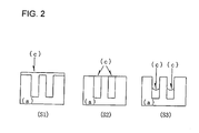
- state of a gap fill material layer formed on a substrate can be controlled by suitably selecting a condition (the kind of the gap fill material forming composition, the kind and concentration of the alkaline aqueous solution, and time) under which the gap fill material layer is etched back with an alkaline aqueous solution. That is, the selection of etch-back condition can provide a state where the gap fill material layer is present also on the substrate ((S1) in Fig. 2), a state where the gap fill material layer is filled only in the inside of holes on the substrate ((S2) in Fig. 2), or a partial fill-state where the gap fill material layer is filled in a part of holes on the substrate ((S3) in Fig. 2).
- a condition the kind of the gap fill material forming composition, the kind and concentration of the alkaline aqueous solution, and time
- the gap fill material layer formed from the gap fill material forming composition according to the present invention is completely removed finally after exposure to light and development of photoresist, and substrate processing, and the like in a process of manufacture of semiconductor device.
- the removal is generally carried out by dry etching.
- dry etching it is generally known that the higher the proportion of aromatic ring structure contained in a layer to be removed is, the lower the removal rate is. Therefore, in case where it is desired to raise the removal rate by dry etching, it is preferable to reduce the amount of aromatic ring structure contained in the gap fill material forming composition used. Particularly, it is preferable to reduce the amount of aromatic ring structure contained in the polymer component.
- a polymer having no aromatic ring structure in the structure thereof is preferably used.
- the polymer includes for example polymers produced from only monomers selected from acrylic acid, methacrylic acid, 2-hydroxyethylmethacrylate and vinyl alcohol, etc.
- it includes polymers obtained by copolymerizing these monomers with monomers selected from alkyl acrylate or alkyl methacrylate such as methyl acrylate, ethyl acrylate, methyl methacrylate, ethyl methacrylate, isopropyl methacrylate, hexyl methacrylate, etc.
- alkyl vinyl ether such as ethyl vinyl ether, ethyl butyl ether, etc.
- alkyl carboxylic acid vinyl ester such as vinyl acetate, vinyl butyrate, etc.
- N-alkylmaleimide such as N-methylmaleimide, N-cyclohexylmaleimide, etc., maleic anhydride, acrylonitrile, and the like.
- the polymer includes polymethacrylic acid, poly(2-hydroxyethyl) methacrylate, polyvinyl alcohol, a copolymerized polymer of acrylic acid with ethyl methacrylate, a copolymerized polymer of vinyl alcohol with butyl vinyl ether, a copolymerized polymer of ethyl methacrylate with 2-hydroxyethyl vinyl ether, a copolymerized polymer of 2-hydroxypropyl methacrylate, propyl acrylate and acrylonitrile, a copolymerized polymer of methacrylic acid, 2-hydroxyethyl methacrylate and ethyl methacrylate, a copolymerized polymer of 2-hydroxyethyl methacrylate, ethyl methacrylate and maleic anhydride, a copolymerized polymer of methacrylic acid, 2-hydroxyethyl methacrylate, methyl methacrylate and N-cyclohexy
- the photoresist includes a positive type photoresist consisting of a novolak resin and 1,2-naphthoquinone diazide sulfonic acid ester, a chemically-amplified type resist which consists of a photoacid generator and a binder having a group which is decomposed with an acid and increases alkali dissolution rate, a chemically-amplified type resist consisting of an alkali-soluble binder, a photoacid generator, and a low molecular compound which is decomposed with an acid and increases the alkali dissolution rate of the photoresist, a chemically-amplified resist consisting of a photoacid generator, a binder having a group which is decomposed with an acid and increases the alkali dissolution rate, and a low molecular compound which is decomposed with a photoacid generator, a binder having a group which is decomposed with an acid and increases the alkali dissolution rate, and a low molecular
- a photoresist is formed, thereafter it can be exposed to light through a predetermined mask, developed, rinsed and dried to obtain a photoresist pattern. If necessary, post exposure bake (PEB) may be performed.
- PEB post exposure bake
- an anti-reflective coating layer may be applied and formed prior to application and forming of the photoresist.
- the anti-reflective coating layer composition used in such a case is not specifically limited, and can be arbitrarily selected from those conventionally used in the prior lithography process, and used.
- the anti-reflective coating can be formed by coating by the conventional method, for example, with a spinner or a coater, and baking.
- the anti-reflective coating composition includes for example one containing as main components a light absorbing compound, a resin and a solvent, one containing as main components a resin having a light absorbing group through chemical bond, a crosslinking agent and a solvent, one containing as main components a light absorbing compound, a crosslinking agent and a solvent, one containing as main components a polymer crosslinking agent having a light absorbing property and a solvent, and the like.
- the anti-reflective coating composition may contain an acid component, an acid generator component, a rheology controlling agent, or the like, if necessary.
- the light absorbing compounds that can be used are any compounds having a high absorption for light at photosensitive characteristic wavelength region of the photosensitive component in the photoresist provided on the anti-reflective coating, and include for example benzophenone compounds, benzotriazole compounds, azo compounds, naphthalene compounds, anthracene compounds, anthraquinone compounds, triazine compounds, and the like.
- the resins include polyesters, polyimides, polystyrenes, novolak resins, polyacetal resins, (meth)acrylic resins, and the like.
- the resins having a light absorbing group through chemical bond include resins having a light absorbing aromatic ring structure such as anthracene ring, naphthalene ring, benzene ring, quinoline ring, quinoxaline ring or thiazole ring.
- the substrates on which the gap fill material forming composition of the present invention is applied are substrates having holes with an aspect ratio shown in height/diameter of 1 or more (for example, silicon/silicon dioxide coat substrate, silicon nitride substrate, glass substrate, ITO substrate or the like) that are conventionally used in the manufacture of semiconductor device.
- the composition can be used for substrates having holes with an aspect ratio less than 1, or substrates having steps in order to flatten the surface thereof. Further, the composition can be used for substrates having no steps.
- these substrates may be substrates on which an inorganic anti-reflective coating is formed by CVD method or the like, and the gap fill material forming composition of the present invention can be coated on the substrate
- the gap fill material layer formed from the gap fill material forming composition of the present invention may contain an absorption for light used in the lithography process.
- the gap fill material layer can act as a layer having a prevent effect against light reflected from the substrate.
- the gap fill material layer of the present invention can be used as a layer for preventing an interaction between the substrate and the photoresist, as a layer having a function that prevents an adverse effect against the substrate by the material used for the photoresist or by substances formed on exposure to light of the photoresist, or as a layer having a function that prevents diffusion substances formed in the substrate on baking under heating to the upper layer photoresist.
- the resulting solution was coated on a silicon wafer by means of a spinner.
- the coated silicon wafer was heated at 120°C for 1 minute on a hot plate to form a gap fill material layer for lithography (film thickness 1.1 ⁇ m).
- the gap fill material layer was dipped in 2.38% tetramethylammonium hydroxide aqueous solution for a predetermined time, and alkali-dissolution rate was measured.
- the alkali-dissolution rate was 18 nm per second when calculated from the dipping time and reduced amount in film thickness.
- the resulting solution was coated on a silicon wafer by means of a spinner.
- the coated silicon wafer was baked at 120°C for 1 minute and then 205°C for 1 minute on a hot plate to form a gap fill material layer for lithography (film thickness 1.0 ⁇ m).
- the gap fill material layer was dipped in a solvent used for a photoresist, such as ethyl lactate, and propylene glycol monomethyl ether, and it was confirmed that the layer was insoluble in the solvent.
- the resulting solution was coated on a silicon wafer having holes (diameter: 0.18 ⁇ m, depth: 1.1 ⁇ m) by means of a spinner.
- the coated silicon wafer was heated at 120°C for 1 minute on a hot plate to form a gap fill material layer for lithography (film thickness 1.1 ⁇ m).
- the flattening property of the resulting gap fill material layer for lithography was assessed by observing with a scanning electron microscope (SEM) the sectional form of the silicon wafer substrate having holes on which the gap fill material layer was formed.
- SEM scanning electron microscope
- the gap fill material layer applied and formed on a silicon wafer having holes was dipped in 2.38% tetramethyl ammonium hydroxide aqueous solution for 55 seconds, and then was heated at 205°C for 1 minute on a hot plate.
- the flattening property of the resulting gap fill material layer for lithography was assessed by observing with a scanning electron microscope (SEM) the sectional form of the silicon wafer substrate having holes on which the gap fill material layer was formed.
- SEM scanning electron microscope
- the resulting solution was coated on a silicon wafer by means of a spinner.
- the coated silicon wafer was heated at 145°C for 1 minute on a hot plate to form a gap fill material layer for lithography (film thickness 1.0 ⁇ m).
- the gap fill material layer was dipped in 2.38% tetramethylammonium hydroxide aqueous solution for a predetermined time, and alkali-dissolution rate was measured.
- the alkali-dissolution rate was 5.0 nm per second when calculated from the dipping time and reduced amount in film thickness.
- the resulting solution was coated on a silicon wafer by means of a spinner.
- the coated silicon wafer was heated at 135°C for 1 minute on a hot plate to form a gap fill material layer for lithography (film thickness 1.0 ⁇ m).
- the gap fill material layer was dipped in 2.38% tetramethylammonium hydroxide aqueous solution for a predetermined time, and alkali-dissolution rate was measured.
- the alkali-dissolution rate was 9.0 nm per second when calculated from the dipping time and reduced amount in film thickness.
- the resulting solution was coated on a silicon wafer by means of a spinner.
- the coated silicon wafer was heated at 135°C for 1 minute or 145°C for 1 minute and then 205°C for 1 minute on a hot plate to form a gap fill material layer for lithography (film thickness 1.0 ⁇ m).
- the gap fill material layer was dipped in a solvent used for a photoresist, such as ethyl lactate, and propylene glycol monomethyl ether, and it was confirmed that the layer was insoluble to the solvent.
- the resulting solution was coated on a silicon wafer having holes (diameter: 0.13 ⁇ m, depth: 0.8 ⁇ m) by means of a spinner.
- the coated silicon wafer was heated at 120°C for 1 minute on a hot plate to form a gap fill material layer for lithography (film thickness 1.0 ⁇ m).
- the flattening property of the resulting gap fill material layer for lithography was assessed by observing with a scanning electron microscope (SEM) the sectional form of the silicon wafer substrate having holes on which the gap fill material layer was formed.
- SEM scanning electron microscope
- the resulting solution was coated on a silicon wafer by means of a spinner.
- the coated silicon wafer was heated at 175°C for 1 minute on a hot plate to form a gap fill material layer for lithography (film thickness 1.0 ⁇ m).
- the gap fill material layer was dipped in 2.38% tetramethylammonium hydroxide aqueous solution for a predetermined time, and alkali-dissolution rate was measured.
- the alkali-dissolution rate was 50 nm per second when calculated from the dipping time and reduced amount in film thickness.
- the resulting solution was coated on a silicon wafer by means of a spinner.
- the coated silicon wafer was heated at 175°C for 1 minute and then 205°C for 1 minute on a hot plate to form a gap fill material layer for lithography (film thickness 1.0 ⁇ m).
- the gap fill material layer was dipped in a solvent used for a photoresist, such as ethyl lactate, and propylene glycol monomethyl ether, and it was confirmed that the layer was insoluble to the solvent.
- the resulting solution was coated on a silicon wafer having holes (diameter: 0.13 ⁇ m, depth: 0.8 ⁇ m) by means of a spinner.
- the coated silicon wafer was heated at 175°C for 1 minute on a hot plate to form a gap fill material layer (film thickness 1.0 ⁇ m).
- the flattening property of the resulting gap fill material layer for lithography was assessed by observing with a scanning electron microscope (SEM) the sectional form of the silicon wafer substrate having holes on which the gap fill material layer was formed.
- SEM scanning electron microscope
Landscapes
- Engineering & Computer Science (AREA)
- Architecture (AREA)
- Structural Engineering (AREA)
- Physics & Mathematics (AREA)
- General Physics & Mathematics (AREA)
- Materials For Photolithography (AREA)
Abstract
Description
- as a first aspect, a gap fill material forming composition characterized in that the composition is used in manufacture of semiconductor device by a method comprising coating a photoresist on a substrate having a hole with aspect ratio shown in height/diameter of 1 or more, and transferring an image to the substrate by use of lithography process, and that the composition is coated on the substrate prior to coating of the photoresist, and comprises a polymer having a hydroxy group or a carboxy group and a crosslinking agent;
- as a second aspect, the gap fill material forming composition as described in the first aspect, wherein the polymer has a weight average molecular weight of 500 to 30000;
- as a third aspect, the gap fill material forming composition as described in the first aspect, wherein the polymer is a polymer containing repeating unit having a hydroxy group or a carboxy group in main chain:
- as a fourth aspect, the gap fill material forming composition as described in the first aspect, wherein the polymer is a polymer containing repeating unit having a hydroxy group or a carboxy group in side chain;
- as a fifth aspect, the gap fill material forming composition as described in the first aspect, wherein the polymer is a polymer containing acrylic acid or methacrylic acid as repeating unit;
- as a sixth aspect, the gap fill material forming composition as described in the first aspect, wherein the polymer is a polymer containing hydroxyalkyl acrylate or hydroxyalkyl methacrylate as repeating unit;
- as a seventh aspect, the gap fill material forming composition as described in the first aspect, wherein the polymer is a dextrin ester compound;
- as an eighth aspect, the gap fill material forming composition as described in the first aspect, wherein the polymer is a polymer containing hydroxystyrene as repeating unit;
- as a ninth aspect, the gap fill material forming composition as described in any one of the first to seventh aspects, wherein the polymer has no aromatic ring structure in the structure;
- as a tenth aspect, the gap fill material forming composition as described in the first aspect, wherein the crosslinking agent is a crosslinking agent having at least two crosslink-forming functional groups;
- as an eleventh aspect, the gap fill material forming composition as described in any one of the first to tenth aspects, further containing an alkali-dissolution rate regulator;
- as a twelfth aspect, a method for forming a gap fill material layer for use in manufacture of semiconductor device comprising coating the gap fill material forming composition as described in any one of the first to eleventh aspects on a substrate and baking it; and
- as a thirteenth aspect, a gap fill material layer manufactured by coating the gap fill material forming composition as described in any one of the first to eleventh aspects on a semiconductor substrate and baking it, in which the gap fill material layer has a dissolution rate for an alkaline aqueous solution having a concentration of 0.1 % to 20% ranging from 3 to 200 nm per second.
The combined use of the monomer having addition polymerization unsaturated bond containing no hydroxy group or carboxy group makes possible to control solubility rate to an alkaline aqueous solution, glass transition temperature, solubility to a solvent, dry etching rate, adhesion with a substrate and resist poisoning resistance or the like of the resulting polymer.

Claims (13)
- A gap fill material forming composition characterized in that the composition is used in manufacture of semiconductor device by a method comprising coating a photoresist on a substrate having a hole with aspect ratio shown in height/diameter of 1 or more, and transferring an image to the substrate by use of lithography process, and that the composition is coated on the substrate prior to coating of the photoresist, and comprises a polymer having a hydroxy group or a carboxy group and a crosslinking agent.
- The gap fill material forming composition according to claim 1, wherein the polymer has a weight average molecular weight of 500 to 30000.
- The gap fill material forming composition according to claim 1, wherein the polymer is a polymer containing repeating unit having a hydroxy group or a carboxy group in main chain.
- The gap fill material forming composition according to claim 1, wherein the polymer is a polymer containing repeating unit having a hydroxy group or a carboxy group in side chain.
- The gap fill material forming composition according to claim 1, wherein the polymer is a polymer containing acrylic acid or methacrylic acid as repeating unit.
- The gap fill material forming composition according to claim 1, wherein the polymer is a polymer containing hydroxyalkyl acrylate or hydroxyalkyl methacrylate as repeating unit.
- The gap fill material forming composition according to claim 1, wherein the polymer is a dextrin ester compound.
- The gap fill material forming composition according to claim 1, wherein the polymer is a polymer containing hydroxystyrene as repeating unit.
- The gap fill material forming composition according to any one of claims 1 to 7, wherein the polymer has no aromatic ring structure in the structure.
- The gap fill material forming composition according to claim 1, wherein the crosslinking agent is a crosslinking agent having at least two crosslink-forming functional groups.
- The gap fill material forming composition according to any one of claims 1 to 10, further containing an alkali-dissolution rate regulator.
- A method for forming a gap fill material layer for use in manufacture of semiconductor device comprising coating the gap fill material forming composition according to any one of claims 1 to 11 on a substrate and baking it.
- A gap fill material layer manufactured by coating the gap fill material forming composition according to any one of claims 1 to 11 on a semiconductor substrate and baking it, in which the gap fill material layer has a dissolution rate for an alkaline aqueous solution having a concentration of 0.1 % to 20% ranging from 3 to 200 nm per second.
Applications Claiming Priority (3)
| Application Number | Priority Date | Filing Date | Title |
|---|---|---|---|
| JP2002376781 | 2002-12-26 | ||
| JP2002376781 | 2002-12-26 | ||
| PCT/JP2003/016735 WO2004061526A1 (en) | 2002-12-26 | 2003-12-25 | Alkali-soluble gap filling material forming composition for lithography |
Publications (3)
| Publication Number | Publication Date |
|---|---|
| EP1586945A1 true EP1586945A1 (en) | 2005-10-19 |
| EP1586945A4 EP1586945A4 (en) | 2009-12-09 |
| EP1586945B1 EP1586945B1 (en) | 2015-07-29 |
Family
ID=32708280
Family Applications (1)
| Application Number | Title | Priority Date | Filing Date |
|---|---|---|---|
| EP03768236.6A Expired - Lifetime EP1586945B1 (en) | 2002-12-26 | 2003-12-25 | Alkali-soluble gap filling material forming composition for lithography |
Country Status (8)
| Country | Link |
|---|---|
| US (1) | US7361718B2 (en) |
| EP (1) | EP1586945B1 (en) |
| JP (1) | JP4210858B2 (en) |
| KR (1) | KR101158297B1 (en) |
| CN (1) | CN1732410B (en) |
| AU (1) | AU2003292809A1 (en) |
| TW (1) | TW200421037A (en) |
| WO (1) | WO2004061526A1 (en) |
Cited By (2)
| Publication number | Priority date | Publication date | Assignee | Title |
|---|---|---|---|---|
| EP1681594A4 (en) * | 2003-10-30 | 2007-06-06 | Nissan Chemical Ind Ltd | COMPOSITION FOR FORMING AN UNDERLYING FILM CONTAINING DEXTRIN ESTER COMPOUND |
| EP2574407A1 (en) * | 2011-09-29 | 2013-04-03 | Fraunhofer-Gesellschaft zur Förderung der angewandten Forschung e.V. | Method for producing a coating of a substrate |
Families Citing this family (19)
| Publication number | Priority date | Publication date | Assignee | Title |
|---|---|---|---|---|
| TWI310484B (en) * | 2003-02-21 | 2009-06-01 | Nissan Chemical Ind Ltd | Composition containing acrylic polymer for forming gap-filling material for lithography |
| US20050160934A1 (en) | 2004-01-23 | 2005-07-28 | Molecular Imprints, Inc. | Materials and methods for imprint lithography |
| US7307118B2 (en) | 2004-11-24 | 2007-12-11 | Molecular Imprints, Inc. | Composition to reduce adhesion between a conformable region and a mold |
| KR100586165B1 (en) * | 2003-12-30 | 2006-06-07 | 동부일렉트로닉스 주식회사 | Floor anti-reflective coating method |
| US20050170638A1 (en) * | 2004-01-30 | 2005-08-04 | Bang-Ching Ho | Method for forming dual damascene interconnect structure |
| US8076386B2 (en) * | 2004-02-23 | 2011-12-13 | Molecular Imprints, Inc. | Materials for imprint lithography |
| KR100596422B1 (en) * | 2004-10-30 | 2006-07-06 | 주식회사 하이닉스반도체 | Manufacturing Method of Semiconductor Device |
| CN101048705B (en) * | 2004-11-01 | 2010-11-10 | 日产化学工业株式会社 | Underlayer film-forming composition for lithography containing cyclodextrin compound |
| JP2006133315A (en) * | 2004-11-02 | 2006-05-25 | Matsushita Electric Ind Co Ltd | Planarizing material, antireflection film forming material, and semiconductor device manufacturing method using the same |
| US8142703B2 (en) | 2005-10-05 | 2012-03-27 | Molecular Imprints, Inc. | Imprint lithography method |
| US7563563B2 (en) * | 2006-04-18 | 2009-07-21 | International Business Machines Corporation | Wet developable bottom antireflective coating composition and method for use thereof |
| KR100792045B1 (en) * | 2006-08-10 | 2008-01-04 | 제일모직주식회사 | Hard mask composition for resist underlayer film and manufacturing method of semiconductor integrated circuit device using same |
| JP4784784B2 (en) * | 2006-08-28 | 2011-10-05 | 日産化学工業株式会社 | Resist underlayer film forming composition containing liquid additive |
| US7651830B2 (en) * | 2007-06-01 | 2010-01-26 | 3M Innovative Properties Company | Patterned photoacid etching and articles therefrom |
| JP6206677B2 (en) * | 2012-12-14 | 2017-10-04 | 日産化学工業株式会社 | Resist underlayer film forming composition containing carbonyl group-containing polyhydroxy aromatic ring novolak resin |
| KR102356815B1 (en) * | 2013-11-14 | 2022-01-27 | 롬 앤드 하스 일렉트로닉 머트어리얼즈 엘엘씨 | Gap-fill methods |
| JP6014110B2 (en) | 2013-12-23 | 2016-10-25 | ダウ グローバル テクノロジーズ エルエルシー | Gap filling method |
| US9324604B2 (en) * | 2014-07-04 | 2016-04-26 | Rohm And Haas Electronic Materials Llc | Gap-fill methods |
| CN109073978B (en) * | 2016-05-02 | 2022-05-17 | 日产化学株式会社 | Composition for forming protective film containing specific crosslinking agent and pattern forming method using the same |
Family Cites Families (13)
| Publication number | Priority date | Publication date | Assignee | Title |
|---|---|---|---|---|
| JPS4867447A (en) | 1971-12-14 | 1973-09-14 | ||
| KR930010248B1 (en) * | 1984-09-14 | 1993-10-15 | 가부시끼가이샤 히다찌세이사꾸쇼 | Pattern Formation Method |
| JPH0727216B2 (en) * | 1985-02-06 | 1995-03-29 | 株式会社日立製作所 | Pattern formation method |
| JPS6170720A (en) * | 1984-09-14 | 1986-04-11 | Hitachi Ltd | Method of forming pattern |
| JPS61205494A (en) | 1985-03-11 | 1986-09-11 | Sanmatsu Kogyo Kk | Production of branched dextrin and straight-chain oligosaccharide |
| US5693691A (en) | 1995-08-21 | 1997-12-02 | Brewer Science, Inc. | Thermosetting anti-reflective coatings compositions |
| JPH10215893A (en) | 1997-02-07 | 1998-08-18 | Masahiro Niimi | Production of dextrin |
| US5919599A (en) * | 1997-09-30 | 1999-07-06 | Brewer Science, Inc. | Thermosetting anti-reflective coatings at deep ultraviolet |
| US6057239A (en) | 1997-12-17 | 2000-05-02 | Advanced Micro Devices, Inc. | Dual damascene process using sacrificial spin-on materials |
| JP2001083705A (en) | 1999-09-14 | 2001-03-30 | Mitsubishi Paper Mills Ltd | Positive photosensitive composition |
| US6461717B1 (en) * | 2000-04-24 | 2002-10-08 | Shipley Company, L.L.C. | Aperture fill |
| US6806161B2 (en) | 2000-04-28 | 2004-10-19 | Lg Chem Investment, Ltd. | Process for preparing insulating material having low dielectric constant |
| JP4654544B2 (en) * | 2000-07-12 | 2011-03-23 | 日産化学工業株式会社 | Gap fill material forming composition for lithography |
-
2003
- 2003-12-25 US US10/540,389 patent/US7361718B2/en not_active Expired - Lifetime
- 2003-12-25 WO PCT/JP2003/016735 patent/WO2004061526A1/en not_active Ceased
- 2003-12-25 CN CN2003801073531A patent/CN1732410B/en not_active Expired - Lifetime
- 2003-12-25 EP EP03768236.6A patent/EP1586945B1/en not_active Expired - Lifetime
- 2003-12-25 AU AU2003292809A patent/AU2003292809A1/en not_active Abandoned
- 2003-12-25 KR KR1020057011811A patent/KR101158297B1/en not_active Expired - Lifetime
- 2003-12-25 JP JP2004564524A patent/JP4210858B2/en not_active Expired - Lifetime
- 2003-12-26 TW TW092137124A patent/TW200421037A/en not_active IP Right Cessation
Cited By (3)
| Publication number | Priority date | Publication date | Assignee | Title |
|---|---|---|---|---|
| EP1681594A4 (en) * | 2003-10-30 | 2007-06-06 | Nissan Chemical Ind Ltd | COMPOSITION FOR FORMING AN UNDERLYING FILM CONTAINING DEXTRIN ESTER COMPOUND |
| US8916327B2 (en) | 2003-10-30 | 2014-12-23 | Nissan Chemical Industries, Ltd. | Underlayer coating forming composition containing dextrin ester compound |
| EP2574407A1 (en) * | 2011-09-29 | 2013-04-03 | Fraunhofer-Gesellschaft zur Förderung der angewandten Forschung e.V. | Method for producing a coating of a substrate |
Also Published As
| Publication number | Publication date |
|---|---|
| WO2004061526A1 (en) | 2004-07-22 |
| US20060041078A1 (en) | 2006-02-23 |
| KR20050094411A (en) | 2005-09-27 |
| JPWO2004061526A1 (en) | 2006-05-18 |
| JP4210858B2 (en) | 2009-01-21 |
| TW200421037A (en) | 2004-10-16 |
| AU2003292809A1 (en) | 2004-07-29 |
| EP1586945B1 (en) | 2015-07-29 |
| TWI316164B (en) | 2009-10-21 |
| KR101158297B1 (en) | 2012-06-26 |
| CN1732410A (en) | 2006-02-08 |
| CN1732410B (en) | 2012-05-02 |
| US7361718B2 (en) | 2008-04-22 |
| EP1586945A4 (en) | 2009-12-09 |
Similar Documents
| Publication | Publication Date | Title |
|---|---|---|
| EP1586945B1 (en) | Alkali-soluble gap filling material forming composition for lithography | |
| EP2343597B1 (en) | Use of an underlayer coating forming composition for lithography | |
| CN102981368B (en) | Antireflective film-forming composition containing vinyl ether compound | |
| KR100875802B1 (en) | Gap-fill Formation Compositions for Lithography | |
| US7365023B2 (en) | Porous underlayer coating and underlayer coating forming composition for forming porous underlayer coating | |
| US8039202B2 (en) | Positive-working photoimageable bottom antireflective coating | |
| US8007979B2 (en) | Acrylic polymer-containing gap fill material forming composition for lithography | |
| JP2004102203A (en) | Antireflection film forming composition | |
| US8916327B2 (en) | Underlayer coating forming composition containing dextrin ester compound | |
| EP1811342B1 (en) | Use of a sulfur-atom-containing composition for forming of lithographic antireflection film |
Legal Events
| Date | Code | Title | Description |
|---|---|---|---|
| PUAI | Public reference made under article 153(3) epc to a published international application that has entered the european phase |
Free format text: ORIGINAL CODE: 0009012 |
|
| 17P | Request for examination filed |
Effective date: 20050715 |
|
| AK | Designated contracting states |
Kind code of ref document: A1 Designated state(s): AT BE BG CH CY CZ DE DK EE ES FI FR GB GR HU IE IT LI LU MC NL PT RO SE SI SK TR |
|
| AX | Request for extension of the european patent |
Extension state: AL LT LV MK |
|
| DAX | Request for extension of the european patent (deleted) | ||
| RBV | Designated contracting states (corrected) |
Designated state(s): DE FR GB IT NL |
|
| A4 | Supplementary search report drawn up and despatched |
Effective date: 20091105 |
|
| 17Q | First examination report despatched |
Effective date: 20100629 |
|
| GRAP | Despatch of communication of intention to grant a patent |
Free format text: ORIGINAL CODE: EPIDOSNIGR1 |
|
| INTG | Intention to grant announced |
Effective date: 20141217 |
|
| RIN1 | Information on inventor provided before grant (corrected) |
Inventor name: ISHII, KAZUHISA Inventor name: ARASE, SHINYA Inventor name: TAKEI, SATOSHI |
|
| GRAP | Despatch of communication of intention to grant a patent |
Free format text: ORIGINAL CODE: EPIDOSNIGR1 |
|
| INTG | Intention to grant announced |
Effective date: 20150304 |
|
| GRAS | Grant fee paid |
Free format text: ORIGINAL CODE: EPIDOSNIGR3 |
|
| GRAA | (expected) grant |
Free format text: ORIGINAL CODE: 0009210 |
|
| AK | Designated contracting states |
Kind code of ref document: B1 Designated state(s): DE FR GB IT NL |
|
| REG | Reference to a national code |
Ref country code: GB Ref legal event code: FG4D |
|
| REG | Reference to a national code |
Ref country code: DE Ref legal event code: R096 Ref document number: 60347875 Country of ref document: DE |
|
| REG | Reference to a national code |
Ref country code: NL Ref legal event code: FP |
|
| REG | Reference to a national code |
Ref country code: FR Ref legal event code: PLFP Year of fee payment: 13 |
|
| PG25 | Lapsed in a contracting state [announced via postgrant information from national office to epo] |
Ref country code: IT Free format text: LAPSE BECAUSE OF FAILURE TO SUBMIT A TRANSLATION OF THE DESCRIPTION OR TO PAY THE FEE WITHIN THE PRESCRIBED TIME-LIMIT Effective date: 20150729 |
|
| REG | Reference to a national code |
Ref country code: DE Ref legal event code: R097 Ref document number: 60347875 Country of ref document: DE |
|
| PLBE | No opposition filed within time limit |
Free format text: ORIGINAL CODE: 0009261 |
|
| STAA | Information on the status of an ep patent application or granted ep patent |
Free format text: STATUS: NO OPPOSITION FILED WITHIN TIME LIMIT |
|
| 26N | No opposition filed |
Effective date: 20160502 |
|
| REG | Reference to a national code |
Ref country code: FR Ref legal event code: PLFP Year of fee payment: 14 |
|
| REG | Reference to a national code |
Ref country code: FR Ref legal event code: PLFP Year of fee payment: 15 |
|
| PGFP | Annual fee paid to national office [announced via postgrant information from national office to epo] |
Ref country code: NL Payment date: 20221114 Year of fee payment: 20 Ref country code: GB Payment date: 20221103 Year of fee payment: 20 Ref country code: FR Payment date: 20221110 Year of fee payment: 20 Ref country code: DE Payment date: 20220622 Year of fee payment: 20 |
|
| REG | Reference to a national code |
Ref country code: DE Ref legal event code: R071 Ref document number: 60347875 Country of ref document: DE |
|
| REG | Reference to a national code |
Ref country code: NL Ref legal event code: MK Effective date: 20231224 |
|
| REG | Reference to a national code |
Ref country code: GB Ref legal event code: PE20 Expiry date: 20231224 |
|
| PG25 | Lapsed in a contracting state [announced via postgrant information from national office to epo] |
Ref country code: GB Free format text: LAPSE BECAUSE OF EXPIRATION OF PROTECTION Effective date: 20231224 |
|
| PG25 | Lapsed in a contracting state [announced via postgrant information from national office to epo] |
Ref country code: GB Free format text: LAPSE BECAUSE OF EXPIRATION OF PROTECTION Effective date: 20231224 |