EP1586673A1 - Component for film forming device and method of washing the component - Google Patents
Component for film forming device and method of washing the component Download PDFInfo
- Publication number
- EP1586673A1 EP1586673A1 EP04704359A EP04704359A EP1586673A1 EP 1586673 A1 EP1586673 A1 EP 1586673A1 EP 04704359 A EP04704359 A EP 04704359A EP 04704359 A EP04704359 A EP 04704359A EP 1586673 A1 EP1586673 A1 EP 1586673A1
- Authority
- EP
- European Patent Office
- Prior art keywords
- film
- component
- adhered
- forming device
- cleaning solution
- Prior art date
- Legal status (The legal status is an assumption and is not a legal conclusion. Google has not performed a legal analysis and makes no representation as to the accuracy of the status listed.)
- Granted
Links
Images


Classifications
-
- H—ELECTRICITY
- H10—SEMICONDUCTOR DEVICES; ELECTRIC SOLID-STATE DEVICES NOT OTHERWISE PROVIDED FOR
- H10P—GENERIC PROCESSES OR APPARATUS FOR THE MANUFACTURE OR TREATMENT OF DEVICES COVERED BY CLASS H10
- H10P14/00—Formation of materials, e.g. in the shape of layers or pillars
- H10P14/20—Formation of materials, e.g. in the shape of layers or pillars of semiconductor materials
-
- H—ELECTRICITY
- H10—SEMICONDUCTOR DEVICES; ELECTRIC SOLID-STATE DEVICES NOT OTHERWISE PROVIDED FOR
- H10P—GENERIC PROCESSES OR APPARATUS FOR THE MANUFACTURE OR TREATMENT OF DEVICES COVERED BY CLASS H10
- H10P72/00—Handling or holding of wafers, substrates or devices during manufacture or treatment thereof
- H10P72/04—Apparatus for manufacture or treatment
- H10P72/0402—Apparatus for fluid treatment
- H10P72/0406—Apparatus for fluid treatment for cleaning followed by drying, rinsing, stripping, blasting or the like
- H10P72/0411—Apparatus for fluid treatment for cleaning followed by drying, rinsing, stripping, blasting or the like for wet cleaning or washing
-
- C—CHEMISTRY; METALLURGY
- C23—COATING METALLIC MATERIAL; COATING MATERIAL WITH METALLIC MATERIAL; CHEMICAL SURFACE TREATMENT; DIFFUSION TREATMENT OF METALLIC MATERIAL; COATING BY VACUUM EVAPORATION, BY SPUTTERING, BY ION IMPLANTATION OR BY CHEMICAL VAPOUR DEPOSITION, IN GENERAL; INHIBITING CORROSION OF METALLIC MATERIAL OR INCRUSTATION IN GENERAL
- C23C—COATING METALLIC MATERIAL; COATING MATERIAL WITH METALLIC MATERIAL; SURFACE TREATMENT OF METALLIC MATERIAL BY DIFFUSION INTO THE SURFACE, BY CHEMICAL CONVERSION OR SUBSTITUTION; COATING BY VACUUM EVAPORATION, BY SPUTTERING, BY ION IMPLANTATION OR BY CHEMICAL VAPOUR DEPOSITION, IN GENERAL
- C23C16/00—Chemical coating by decomposition of gaseous compounds, without leaving reaction products of surface material in the coating, i.e. chemical vapour deposition [CVD] processes
- C23C16/44—Chemical coating by decomposition of gaseous compounds, without leaving reaction products of surface material in the coating, i.e. chemical vapour deposition [CVD] processes characterised by the method of coating
- C23C16/4401—Means for minimising impurities, e.g. dust, moisture or residual gas, in the reaction chamber
- C23C16/4407—Cleaning of reactor or reactor parts by using wet or mechanical methods
-
- H—ELECTRICITY
- H10—SEMICONDUCTOR DEVICES; ELECTRIC SOLID-STATE DEVICES NOT OTHERWISE PROVIDED FOR
- H10P—GENERIC PROCESSES OR APPARATUS FOR THE MANUFACTURE OR TREATMENT OF DEVICES COVERED BY CLASS H10
- H10P52/00—Grinding, lapping or polishing of wafers, substrates or parts of devices
Definitions
- the present invention relates to a component of a film-forming device for forming a variety of thin films consisting of film-forming materials on substrates and a method for cleaning the components.
- LSI large scale integrated circuit
- solar cell and a liquid crystal plasma display are formed in a film-forming device wherein thin films are formed on a substrate using a film-forming material according to a variety of film-forming methods such as vapor deposition, sputtering, CVD and other film-forming techniques.
- the film-forming material is also adhered to the surface of components of film-forming device such as a deposition-inhibiting plate, for instance, a mask for substrates and a frame for supporting wafers, during the thin film-forming process.
- a deposition-inhibiting plate for instance, a mask for substrates and a frame for supporting wafers
- the foregoing film-forming material adhered to such components increases its thickness because of the accumulation thereof and the deposited film may be broken, peeled off and may fall off from the components at a certain point of time. This becomes a cause of dust-generation and the dust may be adhered to the substrate on which a film is just in course of formation and may impair the desired characteristic properties of the resulting film. This would in turn reduce the yield of the semiconductor products thus produced.
- the foregoing cleaning requires the interruption of the film-forming device before the adhered film is broken, peeled off and/or falls off, but it is quite difficult to correctly ascertain the instance when the adhered film is broken, peeled off and/or falls off.
- a problem arises such that the operating efficiency of the film-forming device is considerably reduced.
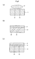
- Fig. 3(a) attached hereto shows a basic material 31 constituting a component of a film-forming device, (hereunder simply referred to as "component"), whose surface is roughened according to a shot blasting technique in which the surface of the basic material is bombarded with steel balls having a small diameter or a glass bead-blasting technique in which glass beads are impacted against the surface thereof.
- component a component of a film-forming device
- Fig. 3(b) attached hereto shows a basic material 32 constituting a component whose surface is roughened according to a mechanical processing method such as cutting and embossing techniques.
- the surface of the basic material 32 undergoes deformation in response to the stress applied onto the adhered film d and liable to cause peeling off of the film to thus relieve the stress. Therefore, any breakage, peeling off and/or falling off of the adhered film d can be prevented.
- Fig.3(c) attached hereto shows a basic material 33, which is first subjected to blasting as has been described above to thus give roughened surface and then coated with a tender metal to form a layer 34 on the surface of the basic material 33.
- the stress which acts on the film d adhered to the component to thus cause breakage, peeling off and/or falling off thereof, can be relaxed because of the presence of such a tender metal layer 34 and accordingly, the latter permits the prevention of any breakage, peeling off and/or falling off of the film d.
- the film adhered to the component is, after all, broken, peeled off and/or falls off from the component, even when using the conventional component having the foregoing structure and accordingly, the component should be cleaned in order to reuse or recycle the same.
- the component has such a structure, which makes any breakage or peeling off and/or falling off of the film adhered thereto, difficult. For this reason, it takes a long period of cleaning time to completely remove the film adhered to the component through the dissolution thereof using a cleaning solution and this in turn results in the substantial reduction of the operational efficiency of the film-forming device.
- the component per se is also immersed in the cleaning solution over a long period of time since a long period of time is required for the removal of the film adhered to the component and the cleaning solution may thus deteriorate the component.
- the component may be replaced with a fresh one.
- a mask for substrates whose size has gradually been increased in response to the need for a large-sized liquid crystal image plane, however, the frequent exchange thereof would instead result in an increase in the cost and labor for the production of thin films. Therefore, there has strongly been desired for the development of a technique, which permits the removal of such a film adhered to the component through cleaning and which makes it possible to reuse the component.
- the component of a film-forming device, according to the present invention in which a thin film is formed on a substrate using a film-forming material, permits the solution of the foregoing problems and it is characterized in that a large number of through holes each extending from the back face to the top face of the component are formed for the penetration of a cleaning solution into the boundary between the component and a film of the film-forming material adhered to the surface of the component and formed during the formation of the foregoing thin film.
- the structure thereof would permit the dissolution of the adhered film not only from the top face thereof, but also from the back face thereof or the boundary between the component and the adhered film, since the cleaning solution likewise comes in contact with the back face of the adhered film through the foregoing through holes. Therefore, the adhered film can be removed from the component prior to the complete dissolution of the same.
- particles of the film-forming material may penetrate into the through holes or the plasma generated during the film-forming step may penetrate into the through holes to thus deposit a film adhered to the body of the device to which the component is attached.
- the through holes is so designed that they have a diameter, which can inhibit the penetration of any particle of the film-forming material or the plasma thereof into the through holes or the foregoing through holes are formed in such a manner that they are in the optically blinded condition with respect to the surface of the component, for instance, the through holes are not vertical to the surface of the component, but are tilted towards the horizontal direction.
- the cleaning solution penetrates into the adhered film not only through the edges of the layer, but also through the through holes and thus, the adhered film can be peeled off from the component within a short period of time.
- the layer serves as a cap, which can inhibit the penetration of any particle of the film-forming material or the plasma thereof into the through holes during the film-forming operation.
- the method for cleaning a component of a film-forming device is characterized in that it comprises the step of immersing, in a cleaning solution, a component having a film consisting of a film-forming material adhered to the surface thereof, wherein the component is a member selected from the group consisting of one having a large number of through holes extending from the back face to the top face of the component; one whose through holes are so designed that they have a diameter capable of inhibiting the penetration of any particle of a film-forming material or the plasma thereof into the through holes; one whose through holes are formed in such a manner that they are not vertical to the surface of the component, but are titled towards the horizontal direction; and one having a layer consisting of a metal film easily soluble in a cleaning solution formed on the surface thereof.
- the cleaning solution in which the component of the film-forming device is immersed penetrates into the adhered film not only through the top face thereof, but also through the back face thereof because of the presence of the through holes to thus dissolve the film and to peel off the same from the component.
- a basic material 1 which is usable to form components in film-forming devices.
- the components which can be formed by the basic material 1 may include a mask for substrate in a film-forming device or a frame for supporting wafer.
- an adhered film d may be formed even over the component of the film-forming device other than the substrate.
- the foregoing adhered film d increases its thickness because of the accumulation thereof and the deposited film may be broken, peeled off and may fall off from the components at a certain point of time. This becomes a cause of dust-generation and the dust may be adhered to the substrate on which a film is just in course of formation and may impair the desired characteristic properties of the resulting film.
- the basic material 1 may be immersed in a cleaning solution S.
- a cleaning solution S can remove the adhered film d only starting from the surface of a component.
- more time was taken in the entire removal of the adhered film d.
- the cleaning solution S is used to dissolve the adhered film d only starting from the surface of the component, it could not but be waited for the adhered film d to be entirely dissolved by the cleaning solution S for removal of the adhered film d since the adhered film d will scarcely be separated from the surface of the component during the cleaning step.
- the basic material 1 may probably be damaged by the cleaning solution S.
- the present invention forms a number of through holes 2 in the basic material 1.
- the structure thereof would permit the dissolution of the adhered film d not only from the top face thereof, but also from the back face thereof or the boundary between the component and the adhered film d, since the cleaning solution likewise comes in contact with the back face of the adhered film d through the through holes 2.
- the cleaning solution S can dissolve and separate the adhered film d from the interface between the adhered film d and the basic material 1 before the adhered film d is entirely dissolved by the cleaning solution S. Therefore, the present invention is advantageous in that the adhered film d can easily and simply be dissolved for a time period which is smaller than time period that would be taken by the prior art to dissolve and remove the adhesion fluid d only starting from the surface of the component.
- the adhered film d can be removed for a shorter time period than that of the prior art, the time period during which the basic material 1 is immersed in the cleaning solution S can be reduced, resulting in less damage to the basic material 1 by the cleaning solution S.
- the number of through holes 2 is especially limited unless it does not damage the strength of the basic material 1.
- the above-mentioned advantage can be provided, for example, if the distance between two adjacent through holes 2 is within the range between 3cm and 5cm.
- Figs. 2 (a)-(c) show enlarged cross-sections of some embodiments of the present invention, each of which has a structure for preventing the particles of the film-forming material and the plasma from entering the through holes 2.
- the present invention is not limited to such forms unless they depart from the spirit and scope of the invention.
- the surfaces of basic materials 11 and 12 shown in Figs. 2(a) and (b) are blast-finished, but may have any other surface structure.
- each through hole 21 is set 0.8mmf so that the plasma P will not enter or pass through the through hole 21.
- the plasma P cannot enter or pass through the through hole 21.
- through hole 22 are formed in such a manner that they are in the optically blinded condition with respect to the surface of the component, for instance, the through hole 22 are not vertical to the surface of the component, but are tilted towards the horizontal direction.
- the particles of the film-forming material or the plasma enter the through holes 22 through their top openings and then impact the inner walls of the through holes 22. Therefore, the particles or plasma cannot almost enter the interior of the through holes 22. This can prevent the adhered film d from accumulating on the main body of the film-forming device on which the components are mounted.
- a basic material 13 which is formed by spraying a layer 14 comprising a metal film having a property of easily-soluble in the cleaning solution.
- this layer 14 serves as a cap, which can inhibit the penetration of any particle of the film-forming material or the plasma thereof into the through hole 12 during the film-forming operation.
- the adhered film d is deposited on the aforementioned layer 14.
- This layer 14 functions to prevent the adhered film d from being broken, peeled off and/or falls off from the substrate by reducing broking/peeling off stresses applied to the adhered film d during formation of the film on the substrate. If the basic material 13 is immersed in the cleaning solution S, however, the layer 14 responds to the cleaning solution S and is dissolved by the cleaning solution S faster than the basic material 13, resulting in separation of the adhered film d from the basic material 13.
- the through holes 23 can cause the cleaning solution S to reach various places in the layer 14. Thus, time required to separate the adhered film d can be reduced in comparison with the prior art.
- the component for the film-forming device according to the present invention and the method of cleaning the component can more easily and simply remove the adhered film for a reduced time period in comparison with the prior art in which the adhered film would be dissolved only starting from the surface thereof, for causing the cleaning solution to enter an interface between the component and the adhered film of the aforementioned film-forming material attached to the surface of the component on formation of the thin-film, by providing a number of through holes extending from the top face of each component to the bottom face of the same.
- the component according to the present invention is suitable for use in the film-forming device for forming a thin-film from a film-forming material on a substrate through any process such as vapor deposition, sputtering, CVD or others, as an anti-adhesion sheet such as a mask for substrate or a frame for supporting wafer.
Landscapes
- Chemical & Material Sciences (AREA)
- Metallurgy (AREA)
- Chemical Kinetics & Catalysis (AREA)
- Engineering & Computer Science (AREA)
- Materials Engineering (AREA)
- Mechanical Engineering (AREA)
- General Chemical & Material Sciences (AREA)
- Organic Chemistry (AREA)
- Cleaning Or Drying Semiconductors (AREA)
- Physical Vapour Deposition (AREA)
- Cleaning In General (AREA)
- Chemical Vapour Deposition (AREA)
- ing And Chemical Polishing (AREA)
Abstract
Description
Adhered film is broken, peeled off and/or falls off, a problem arises such that the operating efficiency of the film-forming device is considerably reduced.
When a thin-film is formed from a film-forming material on a substrate in the film-forming device, an adhered film d may be formed even over the component of the film-forming device other than the substrate.
Claims (8)
- A component of a film-forming device in which a thin film is formed on a substrate using a film-forming material, the component being characterized in that a large number of through holes each extending from the back face to the top face of the component are formed for the penetration of a cleaning solution into the boundary between the component and a film of the film-forming material adhered to the surface of the component and formed during the formation of the foregoing thin film.
- The component of a film-forming device according to claim 1. wherein the through holes of the component is so designed that they have a diameter, which can inhibit the penetration of any particle of the film-forming material or the plasma thereof into the through holes.
- The component of a film-forming device according to claim 1 or 2, wherein the through holes are formed in such a manner that they are not vertical to the surface of the component, but are tilted towards the horizontal direction.
- The component of a film-forming device according to claim 1, wherein a layer consisting of a metal film easily soluble in the cleaning solution is formed on the surface of the component according to a method such as thermal spraying, vapor deposition, sputtering, plating and lamination techniques.
- A method for cleaning a component of a film-forming device comprising the step of immersing, into a cleaning solution, a component as set forth in claim 1 for the removal of a film adhered to the component.
- A method for cleaning a component of a film-forming device comprising the step of immersing, into a cleaning solution, a component as set forth in claim 2 for the removal of a film adhered to the component.
- A method for cleaning a component of a film-forming device comprising the step of immersing, into a cleaning solution, a component as set forth in claim 3 for the removal of a film adhered to the component.
- A method for cleaning a component of a film-forming device comprising the step of immersing , into a cleaning solution, a component as set forth in claim 4 for the removal of a film adhered to the component.
Applications Claiming Priority (3)
| Application Number | Priority Date | Filing Date | Title |
|---|---|---|---|
| JP2003015266 | 2003-01-23 | ||
| JP2003015266 | 2003-01-23 | ||
| PCT/JP2004/000540 WO2004065654A1 (en) | 2003-01-23 | 2004-01-22 | Component for film forming device and method of washing the component |
Publications (3)
| Publication Number | Publication Date |
|---|---|
| EP1586673A1 true EP1586673A1 (en) | 2005-10-19 |
| EP1586673A4 EP1586673A4 (en) | 2012-07-04 |
| EP1586673B1 EP1586673B1 (en) | 2013-04-17 |
Family
ID=32767436
Family Applications (1)
| Application Number | Title | Priority Date | Filing Date |
|---|---|---|---|
| EP04704359.1A Expired - Lifetime EP1586673B1 (en) | 2003-01-23 | 2004-01-22 | Component for film forming device and method of washing the component |
Country Status (9)
| Country | Link |
|---|---|
| US (1) | US7436068B2 (en) |
| EP (1) | EP1586673B1 (en) |
| JP (1) | JP4072920B2 (en) |
| KR (1) | KR101024044B1 (en) |
| CN (1) | CN100476015C (en) |
| CA (1) | CA2511832C (en) |
| MY (1) | MY172602A (en) |
| TW (1) | TWI323288B (en) |
| WO (1) | WO2004065654A1 (en) |
Families Citing this family (4)
| Publication number | Priority date | Publication date | Assignee | Title |
|---|---|---|---|---|
| JP4564434B2 (en) * | 2005-09-30 | 2010-10-20 | Okiセミコンダクタ株式会社 | Semiconductor device and manufacturing method of semiconductor device |
| KR20230091470A (en) | 2021-12-16 | 2023-06-23 | (주)씨엠디엘 | Process for cleaning vapor deposition equipment parts and system for cleaning vapor deposition equipment parts |
| CN116213349A (en) * | 2022-12-07 | 2023-06-06 | 合肥维信诺科技有限公司 | Material recovery device and evaporation device |
| KR20240176280A (en) | 2023-06-15 | 2024-12-24 | (주)씨엠디엘 | Process for cleaning vapor deposition equipment parts and system for cleaning vapor deposition equipment parts |
Family Cites Families (9)
| Publication number | Priority date | Publication date | Assignee | Title |
|---|---|---|---|---|
| JPS62287063A (en) * | 1986-06-03 | 1987-12-12 | Fujitsu Ltd | Method for removing matter sticking to thin film treating equipment |
| JPH05230624A (en) * | 1992-02-20 | 1993-09-07 | Fujitsu Ltd | Method for preventing generation of dust in internal jig of pvd device and internal jig treating apparatus |
| JP3744964B2 (en) * | 1995-04-06 | 2006-02-15 | 株式会社アルバック | Component for film forming apparatus and method for manufacturing the same |
| US6002177A (en) * | 1995-12-27 | 1999-12-14 | International Business Machines Corporation | High density integrated circuit packaging with chip stacking and via interconnections |
| KR100242986B1 (en) * | 1996-11-15 | 2000-02-01 | 김영환 | Muffle installation structure of atmospheric chemical vapor deposition equipment |
| JP3180779B2 (en) * | 1998-10-05 | 2001-06-25 | 日本電気株式会社 | Method for manufacturing semiconductor device |
| US6207553B1 (en) * | 1999-01-26 | 2001-03-27 | Advanced Micro Devices, Inc. | Method of forming multiple levels of patterned metallization |
| JP2000311879A (en) * | 1999-04-28 | 2000-11-07 | Mitsubishi Electric Corp | Cleaning liquid and method for manufacturing semiconductor device using the same |
| JP3876167B2 (en) * | 2002-02-13 | 2007-01-31 | 川崎マイクロエレクトロニクス株式会社 | Cleaning method and semiconductor device manufacturing method |
-
2004
- 2004-01-22 WO PCT/JP2004/000540 patent/WO2004065654A1/en not_active Ceased
- 2004-01-22 US US10/538,087 patent/US7436068B2/en not_active Expired - Lifetime
- 2004-01-22 JP JP2005508116A patent/JP4072920B2/en not_active Expired - Lifetime
- 2004-01-22 CA CA2511832A patent/CA2511832C/en not_active Expired - Lifetime
- 2004-01-22 KR KR1020057010900A patent/KR101024044B1/en not_active Expired - Lifetime
- 2004-01-22 CN CNB2004800023510A patent/CN100476015C/en not_active Expired - Lifetime
- 2004-01-22 EP EP04704359.1A patent/EP1586673B1/en not_active Expired - Lifetime
- 2004-01-26 MY MYPI20040200A patent/MY172602A/en unknown
- 2004-01-27 TW TW093101769A patent/TWI323288B/en not_active IP Right Cessation
Also Published As
| Publication number | Publication date |
|---|---|
| TWI323288B (en) | 2010-04-11 |
| JP4072920B2 (en) | 2008-04-09 |
| CN100476015C (en) | 2009-04-08 |
| CN1738921A (en) | 2006-02-22 |
| EP1586673B1 (en) | 2013-04-17 |
| KR20050118157A (en) | 2005-12-15 |
| KR101024044B1 (en) | 2011-03-22 |
| US20060144418A1 (en) | 2006-07-06 |
| CA2511832C (en) | 2012-01-03 |
| JPWO2004065654A1 (en) | 2006-05-18 |
| MY172602A (en) | 2019-12-05 |
| TW200415244A (en) | 2004-08-16 |
| EP1586673A4 (en) | 2012-07-04 |
| US7436068B2 (en) | 2008-10-14 |
| WO2004065654A1 (en) | 2004-08-05 |
| CA2511832A1 (en) | 2004-08-05 |
Similar Documents
| Publication | Publication Date | Title |
|---|---|---|
| JPH10330971A (en) | Method for manufacturing member for thin film forming apparatus and member for the apparatus | |
| US5755887A (en) | Components of apparatus for film making and method for manufacturing the same | |
| CN101211773B (en) | Method to prevent chip backside metal from peeling off | |
| CA2511832C (en) | Components for a film-forming device and method for cleaning the same | |
| KR20080111967A (en) | Shadow mask | |
| US20060246735A1 (en) | Film-forming apparatus component and method for cleaning same | |
| JP3200650B2 (en) | Manufacturing method of refractory metal film | |
| US6516814B2 (en) | Method of rapid prevention of particle pollution in pre-clean chambers | |
| EP3442008B1 (en) | Protective film forming method for semiconductor substrate | |
| US6599581B2 (en) | Method of fabricating jig for vacuum apparatus | |
| KR102454433B1 (en) | Apparatus of forming a film and cleaning method thereof | |
| JPH11124661A (en) | Component parts for film forming equipment | |
| JP4519416B2 (en) | Anti-contamination device for thin film forming equipment | |
| JP2830633B2 (en) | Method for manufacturing semiconductor device | |
| JP2004303630A (en) | Glass substrate, glass substrate processing method, and organic EL display | |
| JPH06220600A (en) | Washing method of vacuum thin film forming device or the like | |
| JPH0462921A (en) | Etching of rear surface of semiconductor material | |
| JPH03166361A (en) | Thin film forming device | |
| JPH08277469A (en) | Wafer clamp device recycling method | |
| KR102095101B1 (en) | Patch for Recovery of Valuable Metal | |
| US20020153022A1 (en) | Method for preventing particles in a pre-clean chamber | |
| JP2021017609A (en) | Sputtering target and manufacturing method of the same | |
| KR20020091336A (en) | method for removing titanium and titanium nitride deposited on titanium collimator using sacrificeal layer | |
| KR20010009556A (en) | Reusable collimator with multi- layer construction | |
| JP2013251370A (en) | Substrate loading apparatus |
Legal Events
| Date | Code | Title | Description |
|---|---|---|---|
| PUAI | Public reference made under article 153(3) epc to a published international application that has entered the european phase |
Free format text: ORIGINAL CODE: 0009012 |
|
| 17P | Request for examination filed |
Effective date: 20050614 |
|
| AK | Designated contracting states |
Kind code of ref document: A1 Designated state(s): AT BE BG CH CY CZ DE DK EE ES FI FR GB GR HU IE IT LI LU MC NL PT RO SE SI SK TR |
|
| AX | Request for extension of the european patent |
Extension state: AL LT LV MK |
|
| DAX | Request for extension of the european patent (deleted) | ||
| RBV | Designated contracting states (corrected) |
Designated state(s): DE FR GB |
|
| A4 | Supplementary search report drawn up and despatched |
Effective date: 20120601 |
|
| RIC1 | Information provided on ipc code assigned before grant |
Ipc: C23C 14/00 20060101AFI20120525BHEP Ipc: B08B 3/08 20060101ALI20120525BHEP Ipc: C23C 16/44 20060101ALI20120525BHEP Ipc: C23C 16/00 20060101ALI20120525BHEP |
|
| GRAP | Despatch of communication of intention to grant a patent |
Free format text: ORIGINAL CODE: EPIDOSNIGR1 |
|
| RIC1 | Information provided on ipc code assigned before grant |
Ipc: H01L 21/67 20060101ALI20121018BHEP Ipc: B08B 3/08 20060101ALI20121018BHEP Ipc: C23C 14/00 20060101AFI20121018BHEP Ipc: C23C 16/44 20060101ALI20121018BHEP Ipc: C23C 16/00 20060101ALI20121018BHEP |
|
| GRAS | Grant fee paid |
Free format text: ORIGINAL CODE: EPIDOSNIGR3 |
|
| GRAA | (expected) grant |
Free format text: ORIGINAL CODE: 0009210 |
|
| AK | Designated contracting states |
Kind code of ref document: B1 Designated state(s): DE FR GB |
|
| REG | Reference to a national code |
Ref country code: GB Ref legal event code: FG4D |
|
| REG | Reference to a national code |
Ref country code: DE Ref legal event code: R096 Ref document number: 602004041769 Country of ref document: DE Effective date: 20130606 |
|
| PLBE | No opposition filed within time limit |
Free format text: ORIGINAL CODE: 0009261 |
|
| STAA | Information on the status of an ep patent application or granted ep patent |
Free format text: STATUS: NO OPPOSITION FILED WITHIN TIME LIMIT |
|
| 26N | No opposition filed |
Effective date: 20140120 |
|
| REG | Reference to a national code |
Ref country code: DE Ref legal event code: R097 Ref document number: 602004041769 Country of ref document: DE Effective date: 20140120 |
|
| REG | Reference to a national code |
Ref country code: FR Ref legal event code: PLFP Year of fee payment: 13 |
|
| REG | Reference to a national code |
Ref country code: FR Ref legal event code: PLFP Year of fee payment: 14 |
|
| REG | Reference to a national code |
Ref country code: FR Ref legal event code: PLFP Year of fee payment: 15 |
|
| PGFP | Annual fee paid to national office [announced via postgrant information from national office to epo] |
Ref country code: FR Payment date: 20230124 Year of fee payment: 20 |
|
| PGFP | Annual fee paid to national office [announced via postgrant information from national office to epo] |
Ref country code: GB Payment date: 20230119 Year of fee payment: 20 Ref country code: DE Payment date: 20230123 Year of fee payment: 20 |
|
| REG | Reference to a national code |
Ref country code: DE Ref legal event code: R071 Ref document number: 602004041769 Country of ref document: DE |
|
| REG | Reference to a national code |
Ref country code: GB Ref legal event code: PE20 Expiry date: 20240121 |
|
| PG25 | Lapsed in a contracting state [announced via postgrant information from national office to epo] |
Ref country code: GB Free format text: LAPSE BECAUSE OF EXPIRATION OF PROTECTION Effective date: 20240121 |