EP1585604B1 - Industrielles mikroauftragesystem mit auftrageverteilung zur verminderung der auswirkung von tröpfchenausrichtungstoleranzen und -fehlern sowie tröpfchenvolumentoleranzen und -fehlern - Google Patents
Industrielles mikroauftragesystem mit auftrageverteilung zur verminderung der auswirkung von tröpfchenausrichtungstoleranzen und -fehlern sowie tröpfchenvolumentoleranzen und -fehlern Download PDFInfo
- Publication number
- EP1585604B1 EP1585604B1 EP02795705A EP02795705A EP1585604B1 EP 1585604 B1 EP1585604 B1 EP 1585604B1 EP 02795705 A EP02795705 A EP 02795705A EP 02795705 A EP02795705 A EP 02795705A EP 1585604 B1 EP1585604 B1 EP 1585604B1
- Authority
- EP
- European Patent Office
- Prior art keywords
- microdeposition
- head
- nozzles
- mask
- substrate
- Prior art date
- Legal status (The legal status is an assumption and is not a legal conclusion. Google has not performed a legal analysis and makes no representation as to the accuracy of the status listed.)
- Expired - Lifetime
Links
- 230000000873 masking effect Effects 0.000 title description 4
- 239000000758 substrate Substances 0.000 claims abstract description 80
- 239000000463 material Substances 0.000 claims abstract description 50
- 239000012530 fluid Substances 0.000 claims abstract description 44
- 230000007547 defect Effects 0.000 claims abstract description 9
- 238000000034 method Methods 0.000 claims description 41
- 239000010410 layer Substances 0.000 claims description 24
- 238000010304 firing Methods 0.000 claims description 23
- 229920000642 polymer Polymers 0.000 claims description 15
- 238000000151 deposition Methods 0.000 claims description 13
- 239000002365 multiple layer Substances 0.000 claims description 9
- 229910000679 solder Inorganic materials 0.000 claims description 6
- 239000003990 capacitor Substances 0.000 claims description 4
- 239000004020 conductor Substances 0.000 claims description 3
- 239000012212 insulator Substances 0.000 claims description 3
- 238000007747 plating Methods 0.000 claims description 3
- 239000003086 colorant Substances 0.000 claims 2
- 230000006870 function Effects 0.000 abstract description 7
- 239000011295 pitch Substances 0.000 description 14
- 238000004519 manufacturing process Methods 0.000 description 11
- 238000000206 photolithography Methods 0.000 description 8
- 229920002120 photoresistant polymer Polymers 0.000 description 8
- 230000015572 biosynthetic process Effects 0.000 description 6
- 238000001723 curing Methods 0.000 description 5
- 238000000608 laser ablation Methods 0.000 description 5
- 238000004528 spin coating Methods 0.000 description 5
- 230000008021 deposition Effects 0.000 description 4
- 239000000976 ink Substances 0.000 description 4
- 238000007650 screen-printing Methods 0.000 description 3
- 239000002904 solvent Substances 0.000 description 3
- 230000007423 decrease Effects 0.000 description 2
- 230000003247 decreasing effect Effects 0.000 description 2
- 238000010586 diagram Methods 0.000 description 2
- 238000012015 optical character recognition Methods 0.000 description 2
- 230000003287 optical effect Effects 0.000 description 2
- 229920001609 Poly(3,4-ethylenedioxythiophene) Polymers 0.000 description 1
- 238000003848 UV Light-Curing Methods 0.000 description 1
- 230000002411 adverse Effects 0.000 description 1
- 238000000203 droplet dispensing Methods 0.000 description 1
- 238000001035 drying Methods 0.000 description 1
- 230000000694 effects Effects 0.000 description 1
- 239000011521 glass Substances 0.000 description 1
- 230000005525 hole transport Effects 0.000 description 1
- 239000004973 liquid crystal related substance Substances 0.000 description 1
- 230000005389 magnetism Effects 0.000 description 1
- 238000003801 milling Methods 0.000 description 1
- 238000012986 modification Methods 0.000 description 1
- 230000004048 modification Effects 0.000 description 1
- 238000012634 optical imaging Methods 0.000 description 1
- 229920000058 polyacrylate Polymers 0.000 description 1
- 229920000767 polyaniline Polymers 0.000 description 1
- 230000000135 prohibitive effect Effects 0.000 description 1
- 230000002829 reductive effect Effects 0.000 description 1
- 238000000926 separation method Methods 0.000 description 1
- 238000003860 storage Methods 0.000 description 1
- 230000001360 synchronised effect Effects 0.000 description 1
- 230000001960 triggered effect Effects 0.000 description 1
- 238000009966 trimming Methods 0.000 description 1
- 230000000007 visual effect Effects 0.000 description 1
Images


Classifications
-
- B—PERFORMING OPERATIONS; TRANSPORTING
- B41—PRINTING; LINING MACHINES; TYPEWRITERS; STAMPS
- B41J—TYPEWRITERS; SELECTIVE PRINTING MECHANISMS, i.e. MECHANISMS PRINTING OTHERWISE THAN FROM A FORME; CORRECTION OF TYPOGRAPHICAL ERRORS
- B41J2/00—Typewriters or selective printing mechanisms characterised by the printing or marking process for which they are designed
- B41J2/005—Typewriters or selective printing mechanisms characterised by the printing or marking process for which they are designed characterised by bringing liquid or particles selectively into contact with a printing material
- B41J2/01—Ink jet
- B41J2/015—Ink jet characterised by the jet generation process
- B41J2/04—Ink jet characterised by the jet generation process generating single droplets or particles on demand
- B41J2/045—Ink jet characterised by the jet generation process generating single droplets or particles on demand by pressure, e.g. electromechanical transducers
- B41J2/04501—Control methods or devices therefor, e.g. driver circuits, control circuits
- B41J2/04591—Width of the driving signal being adjusted
-
- B—PERFORMING OPERATIONS; TRANSPORTING
- B41—PRINTING; LINING MACHINES; TYPEWRITERS; STAMPS
- B41J—TYPEWRITERS; SELECTIVE PRINTING MECHANISMS, i.e. MECHANISMS PRINTING OTHERWISE THAN FROM A FORME; CORRECTION OF TYPOGRAPHICAL ERRORS
- B41J2/00—Typewriters or selective printing mechanisms characterised by the printing or marking process for which they are designed
- B41J2/005—Typewriters or selective printing mechanisms characterised by the printing or marking process for which they are designed characterised by bringing liquid or particles selectively into contact with a printing material
- B41J2/01—Ink jet
- B41J2/015—Ink jet characterised by the jet generation process
- B41J2/04—Ink jet characterised by the jet generation process generating single droplets or particles on demand
- B41J2/045—Ink jet characterised by the jet generation process generating single droplets or particles on demand by pressure, e.g. electromechanical transducers
- B41J2/04501—Control methods or devices therefor, e.g. driver circuits, control circuits
- B41J2/04505—Control methods or devices therefor, e.g. driver circuits, control circuits aiming at correcting alignment
-
- B—PERFORMING OPERATIONS; TRANSPORTING
- B41—PRINTING; LINING MACHINES; TYPEWRITERS; STAMPS
- B41J—TYPEWRITERS; SELECTIVE PRINTING MECHANISMS, i.e. MECHANISMS PRINTING OTHERWISE THAN FROM A FORME; CORRECTION OF TYPOGRAPHICAL ERRORS
- B41J2/00—Typewriters or selective printing mechanisms characterised by the printing or marking process for which they are designed
- B41J2/005—Typewriters or selective printing mechanisms characterised by the printing or marking process for which they are designed characterised by bringing liquid or particles selectively into contact with a printing material
- B41J2/01—Ink jet
- B41J2/015—Ink jet characterised by the jet generation process
- B41J2/04—Ink jet characterised by the jet generation process generating single droplets or particles on demand
- B41J2/045—Ink jet characterised by the jet generation process generating single droplets or particles on demand by pressure, e.g. electromechanical transducers
- B41J2/04501—Control methods or devices therefor, e.g. driver circuits, control circuits
- B41J2/04506—Control methods or devices therefor, e.g. driver circuits, control circuits aiming at correcting manufacturing tolerances
-
- B—PERFORMING OPERATIONS; TRANSPORTING
- B41—PRINTING; LINING MACHINES; TYPEWRITERS; STAMPS
- B41J—TYPEWRITERS; SELECTIVE PRINTING MECHANISMS, i.e. MECHANISMS PRINTING OTHERWISE THAN FROM A FORME; CORRECTION OF TYPOGRAPHICAL ERRORS
- B41J2/00—Typewriters or selective printing mechanisms characterised by the printing or marking process for which they are designed
- B41J2/005—Typewriters or selective printing mechanisms characterised by the printing or marking process for which they are designed characterised by bringing liquid or particles selectively into contact with a printing material
- B41J2/01—Ink jet
- B41J2/015—Ink jet characterised by the jet generation process
- B41J2/04—Ink jet characterised by the jet generation process generating single droplets or particles on demand
- B41J2/045—Ink jet characterised by the jet generation process generating single droplets or particles on demand by pressure, e.g. electromechanical transducers
- B41J2/04501—Control methods or devices therefor, e.g. driver circuits, control circuits
- B41J2/0458—Control methods or devices therefor, e.g. driver circuits, control circuits controlling heads based on heating elements forming bubbles
-
- B—PERFORMING OPERATIONS; TRANSPORTING
- B41—PRINTING; LINING MACHINES; TYPEWRITERS; STAMPS
- B41J—TYPEWRITERS; SELECTIVE PRINTING MECHANISMS, i.e. MECHANISMS PRINTING OTHERWISE THAN FROM A FORME; CORRECTION OF TYPOGRAPHICAL ERRORS
- B41J2/00—Typewriters or selective printing mechanisms characterised by the printing or marking process for which they are designed
- B41J2/005—Typewriters or selective printing mechanisms characterised by the printing or marking process for which they are designed characterised by bringing liquid or particles selectively into contact with a printing material
- B41J2/01—Ink jet
- B41J2/015—Ink jet characterised by the jet generation process
- B41J2/04—Ink jet characterised by the jet generation process generating single droplets or particles on demand
- B41J2/045—Ink jet characterised by the jet generation process generating single droplets or particles on demand by pressure, e.g. electromechanical transducers
- B41J2/04501—Control methods or devices therefor, e.g. driver circuits, control circuits
- B41J2/04581—Control methods or devices therefor, e.g. driver circuits, control circuits controlling heads based on piezoelectric elements
-
- B—PERFORMING OPERATIONS; TRANSPORTING
- B41—PRINTING; LINING MACHINES; TYPEWRITERS; STAMPS
- B41J—TYPEWRITERS; SELECTIVE PRINTING MECHANISMS, i.e. MECHANISMS PRINTING OTHERWISE THAN FROM A FORME; CORRECTION OF TYPOGRAPHICAL ERRORS
- B41J2/00—Typewriters or selective printing mechanisms characterised by the printing or marking process for which they are designed
- B41J2/005—Typewriters or selective printing mechanisms characterised by the printing or marking process for which they are designed characterised by bringing liquid or particles selectively into contact with a printing material
- B41J2/01—Ink jet
- B41J2/015—Ink jet characterised by the jet generation process
- B41J2/04—Ink jet characterised by the jet generation process generating single droplets or particles on demand
- B41J2/045—Ink jet characterised by the jet generation process generating single droplets or particles on demand by pressure, e.g. electromechanical transducers
- B41J2/04501—Control methods or devices therefor, e.g. driver circuits, control circuits
- B41J2/04588—Control methods or devices therefor, e.g. driver circuits, control circuits using a specific waveform
-
- B—PERFORMING OPERATIONS; TRANSPORTING
- B41—PRINTING; LINING MACHINES; TYPEWRITERS; STAMPS
- B41J—TYPEWRITERS; SELECTIVE PRINTING MECHANISMS, i.e. MECHANISMS PRINTING OTHERWISE THAN FROM A FORME; CORRECTION OF TYPOGRAPHICAL ERRORS
- B41J2/00—Typewriters or selective printing mechanisms characterised by the printing or marking process for which they are designed
- B41J2/005—Typewriters or selective printing mechanisms characterised by the printing or marking process for which they are designed characterised by bringing liquid or particles selectively into contact with a printing material
- B41J2/01—Ink jet
- B41J2/21—Ink jet for multi-colour printing
- B41J2/2132—Print quality control characterised by dot disposition, e.g. for reducing white stripes or banding
-
- H—ELECTRICITY
- H05—ELECTRIC TECHNIQUES NOT OTHERWISE PROVIDED FOR
- H05K—PRINTED CIRCUITS; CASINGS OR CONSTRUCTIONAL DETAILS OF ELECTRIC APPARATUS; MANUFACTURE OF ASSEMBLAGES OF ELECTRICAL COMPONENTS
- H05K3/00—Apparatus or processes for manufacturing printed circuits
- H05K3/10—Apparatus or processes for manufacturing printed circuits in which conductive material is applied to the insulating support in such a manner as to form the desired conductive pattern
- H05K3/12—Apparatus or processes for manufacturing printed circuits in which conductive material is applied to the insulating support in such a manner as to form the desired conductive pattern using thick film techniques, e.g. printing techniques to apply the conductive material or similar techniques for applying conductive paste or ink patterns
- H05K3/1241—Apparatus or processes for manufacturing printed circuits in which conductive material is applied to the insulating support in such a manner as to form the desired conductive pattern using thick film techniques, e.g. printing techniques to apply the conductive material or similar techniques for applying conductive paste or ink patterns by ink-jet printing or drawing by dispensing
- H05K3/125—Apparatus or processes for manufacturing printed circuits in which conductive material is applied to the insulating support in such a manner as to form the desired conductive pattern using thick film techniques, e.g. printing techniques to apply the conductive material or similar techniques for applying conductive paste or ink patterns by ink-jet printing or drawing by dispensing by ink-jet printing
-
- H—ELECTRICITY
- H10—SEMICONDUCTOR DEVICES; ELECTRIC SOLID-STATE DEVICES NOT OTHERWISE PROVIDED FOR
- H10K—ORGANIC ELECTRIC SOLID-STATE DEVICES
- H10K71/00—Manufacture or treatment specially adapted for the organic devices covered by this subclass
- H10K71/10—Deposition of organic active material
- H10K71/12—Deposition of organic active material using liquid deposition, e.g. spin coating
- H10K71/13—Deposition of organic active material using liquid deposition, e.g. spin coating using printing techniques, e.g. ink-jet printing or screen printing
- H10K71/135—Deposition of organic active material using liquid deposition, e.g. spin coating using printing techniques, e.g. ink-jet printing or screen printing using ink-jet printing
-
- H—ELECTRICITY
- H10—SEMICONDUCTOR DEVICES; ELECTRIC SOLID-STATE DEVICES NOT OTHERWISE PROVIDED FOR
- H10K—ORGANIC ELECTRIC SOLID-STATE DEVICES
- H10K71/00—Manufacture or treatment specially adapted for the organic devices covered by this subclass
- H10K71/10—Deposition of organic active material
- H10K71/16—Deposition of organic active material using physical vapour deposition [PVD], e.g. vacuum deposition or sputtering
- H10K71/166—Deposition of organic active material using physical vapour deposition [PVD], e.g. vacuum deposition or sputtering using selective deposition, e.g. using a mask
-
- H—ELECTRICITY
- H10—SEMICONDUCTOR DEVICES; ELECTRIC SOLID-STATE DEVICES NOT OTHERWISE PROVIDED FOR
- H10K—ORGANIC ELECTRIC SOLID-STATE DEVICES
- H10K71/00—Manufacture or treatment specially adapted for the organic devices covered by this subclass
Definitions
- the present invention relates to microdeposition systems, and more particularly to a mask generator for microdeposition systems used to fabricate printed circuit boards, polymer light emitting diode (PLED) displays, and other electronic devices requiring microdeposition of fluid materials.
- PLED polymer light emitting diode
- a microdeposition method and a microdeposition system according to the preambles of claims 1 and 18, respectively, are known from the European Patent Application EP0863778 .
- microstructures that have stall feature sizes on substrates.
- the microstructures form one of more layers of an electronic circuit Examples of these structures include polymer light emitting diode (PILED) display devices, liquid crystal display (LCD) devices, printed circuit boards and the like.
- PILED polymer light emitting diode
- LCD liquid crystal display
- Most of these manufacturing techniques are relatively expensive to implement and require high production quantities to amortize the cost of the fabrication equipment.
- Techniques for forming microstructures one a substrate include screen printing. During screen printing, a fine mesh screen is positioned on the substrate. Fluid material is microdeposited through the screen and onto the substrate in a pattern defined by the screen. Screen printing requires contact between the screen and the substrate. Contact also occurs between the screen and the fluid material, which contaminates both the substrate and the fluid material.
- Photolithography is another manufacturing technique that is used to manufacture microstructures on substrates. Photolithography is also not compatible with the fabrication of some devices. Manufacturing processes using photolithography generally involve the deposition of a photoresist material onto a substrate. The photoresist material is cured by exposure to light. A patterned mask is used to selectively apply light to the photo resist material. Photoresist that is exposed to the light is cured and unexposed portions are not cured. The uncured portions are removed from the substrate. An underlying surface of the substrate is exposed through the removed photoresist layer. The cured portions of the photoresist layer remain on the substrate. Another material is then microdeposited onto the substrate through the opened pattern on the photoresist layer, followed by the removal of the cured portion of the photoresist layer.
- Photolithography has been used successfully to manufacture many microstructures such as traces on circuit boards.
- photolithography contaminates the substrate and the material formed on the substrate.
- the cost of the photolithography process can be prohibitive when relatively small quantities are to be fabricated.
- Spin coating has also been used to form microstructures.
- Spin coating involves rotating a substrate while depositing fluid material at the center of the substrate. The rotational motion of the substrate causes the fluid material to spread uniformly across the surface of the substrate.
- Spin coating is also an expensive process because a majority of the fluid material does not remain on the substrate. Additional material is wasfed due to the requirement that the entire surface of the substrate must be coated with a uniform layer.
- laser ablation can be used to remove material, laser ablation requires expensive equipment. Laser ablation may also create ash, which contaminates the substrate.
- the size of the substrate is limited by the spin coating process to less than approximately 12", which makes spin coating unsuitable for larger devices such as PLED televisions.
- a microdeposition system and method according to the present invention is defined in the claims.
- Such a system and method microdeposits droplets of fluid material to form a feature pattern on a substrate.
- the feature pattern for the substrate is initially defined.
- a mask is created for the feature pattern that reduces a density of defects that occur due to tolerance variations and/or a malfunctioning nozzle of the microdeposition head.
- the droplets of fluid material are microdeposited onto the substrate based on the mask to define sub-features of the feature pattern.
- one of the nozzles of the microdeposition head is assigned to each of the sub-features in the feature pattern.
- the step of assigning nozzles may include randomizing an assigned nozzle for the sub-features.
- the assigned nozzles in the mask are also assigned to one of a plurality of passes of the microdeposition head.
- the Microdeposition pass is performed by at least one of moving the microdeposition head in a linear direction relative to the substrate and moving the substrate in a linear direction relative to the microdeposition head.
- At least one of the sub-features is formed by multiple droplets that are microdeposited in layers.
- the mask assigns a different nozzle to each of the layers of the multiple-layer sub-feature.
- the feature pattern may define a component of an electrical device.
- the electrical device may be one of a polymer light emitting diode, a light panel, an integrated circuit package and a printed circuit board.
- the droplets may form at least one of a light emitter, an electrical conductor, an electrical trace, an insulator, solder bumps, bondwire, plating, interconnects, a capacitor and a resistor.
- the mask increases a number of microdeposition passes required to microdeposit the feature pattern and reduces repeated firing of nozzles of the microdeposition head during each of the microdeposition passes.
- FIG. 1 is a functional block diagram of an exemplary microdeposition system according to the present invention
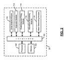
- FIG. 2 is a functional block diagram of a controller including a mask generating module for the microdeposition system of FIG. 1 ;
- FIG. 3 illustrates a waveform generator that is capable of generating different firing waveforms for each nozzle
- FIG. 4 illustrates rise slope, duration, timing and fall slope of an exemplary nozzle firing waveform
- FIGs. 5A and 5B illustrates pitch adjustment of the microdeposition head
- FIG. 6 illustrates an exemplary feature pattern to be microdeposited onto a substrate including sub-features that are defined by droplets of fluid material
- FIG. 7 illustrates a portion of the feature pattern in FIG. 6 ;
- FIG. 8 illustrates microdeposition of sub-features of the portion on the substrate in a single pass using microdeposition without masking
- FIG. 9 illustrates microdeposition of sub-features on the substrate with an exemplary mask to reduce the impact of defects due to nozzle misalignment and/or improper drop formation of one or more nozzles;
- FiGs. 10-22 illustrate successive passes for depositing additional sub-features of the exemplary mask in FIG. 9 ;
- FIG. 23 illustrates a feature pattern including sub-features defined by multiple droplet layers
- FIG. 24 illustrates deposition of a multiple layer sub-feature in the feature pattern of FIG. 23 using the same nozzle to microdeposit all of the layers;
- FIG. 25 illustrates deposition of the multiple layer sub-feature in the feature pattern of FIG. 23 by varying nozzles used to microdeposit the different layers;
- FIG. 26 illustrates an exemplary polymer light-emitting diode (PLED) display device
- FIG. 27 illustrates microdeposition of red, green and blue components forming a pixel using a first method
- FIG. 28 illustrates microdeposition of red, green and blue pixel components forming pixels using the masking method according fo the present invention.
- Microdeposition of fluid materials onto a substrate is disclosed in detail in commonly assigned applications entitled “Interchangeable Microdeposition Head Apparatus and Method". Serial No. 10/479,322, filed November 26. 2003 . now abandoned; "Waveform Generator for Microdeposition Control System", Serial No. 10/479,323, filed June 17, 2004 , now U.S. Patent No. 7.449.070 ; "Over-Clocking in a Microdeposition Control System to Improve Resolution", Serial No. 10/479,316, filed June 14, 2004 , now U.S. Patent No. 7.244.310 ; and "Industrial Microdeposition Systems for Polymer Light Emitting Diode Displays, Printed Circuit Boards and the Like", Serial No. 10/479,318, filed August 18, 2004 , now U.S. Patent No. 7.270.712 .
- the present invention generates a mask that alters a relationship between nozzles of the microdeposition head that are assigned to microdeposit sub-features in the feature pattern to reduce (or de-localize) the impact of nozzles that are both functioning and malfunctioning.
- malfunctioning refers to nozzles that are misaligned outside of a desired tolerance or specification and/or have droplet formation/volume that is outside of a desired specification.
- functioning shall refer to nozzles that are within the desired tolerance or specification and have droplet formation/volume that is within the desired specification.
- functioning nozzles may have a tolerance of +/- 5% for alignment and/or drop volume. These tolerances can correspond to a difference of 10% between adjacent nozzles, which may cause problems for some devices formed by microdeposition. Further, the difference between a malfunctioning nozzle and a functioning nozzle can exceed 10%, which also may cause problems for some devices formed by microdeposition.
- FIGs. 1-5 illustrate an exemplary microdeposition system 20.
- a microdeposition system 20 is illustrated and includes a controller 22, a head assembly 24, and a substrate assembly 26.
- a rotational position or pitch of the head assembly 24 is adjusted using an optional rotary position motor 30 and an optional rotary position sensor 32. Manual adjustment can also be performed.
- a height of the head assembly 24 relative to the substrate assembly 26 may be adjusted using a height adjustment motor 34 and a height sensor 36.
- a lateral position of the head assembly 24 is adjusted using a lateral position motor 40 and a lateral position sensor 42. Manual height and lateral position may be performed to reduce cost.
- a microdeposition head 50 with a plurality of nozzles is mounted on the head assembly 24.
- a first camera 52 is optionally mounted on the head assembly 24. The first camera 52 is used to position the head assembly 24 relative to a substrate 53 that is located on the substrate assembly 26. More particularly, the first camera 52 is used to align the microdeposition head 50 using one or more nozzles of the head 50 as a reference. In addition, the first camera 52 is used to perform drop analysis on the substrate.
- a laser 60 can optionally be used for laser ablation of applied fluid material to reduce minimum feature sizes and/or for creating vias. While the laser 60 is mounted on the head assembly 24 in FIG. 1 , the laser 60 can be mounted on a laser assembly (not shown) that moves independently from the head assembly 24.
- a fluid supply 62 is connected by one or more conduits 63 to the microdeposition head 50.
- the fluid supply 62 provides one or more types of fluid materials, such as polymer PPV for red, green and blue pixels, solvent, resistive fluid materials, conductive fluid materials, resist fluid materials, and/or insulating fluid materials.
- the fluid supply 62 is optionally capable of changing the fluid material that is supplied by using a solvent flush before switching to a new fluid material.
- a lateral position motor 64 and a lateral position sensor 66 are used to position the substrate assembly 26 with respect to the head assembly 24.
- the lateral position motor 40 moves along a first axis.
- the lateral position motor 64 moves along a second axis that is perpendicular to the first axis.
- the position motors 30, 34, 40 and 64 are associated with either the head assembly 24 or the substrate assembly 26. In other words, the degrees of relative movement and rotation may be provided by moving or rotating the substrate assembly 26 and/or the head assembly 24 and any combination thereof.
- a blotting station 70 and a blotting media motor 72 are preferably located adjacent to the substrate assembly 26. To prevent clogging of nozzles of the microdeposition head 50, the microdeposition head 50 is cleaned periodically during use. The microdeposition head 50 is moved into position over the blotting station 70 and a nozzle plate (not shown) of the microdeposition head is wiped on the blotting station 70.
- the blotting station 70 includes a roll of blotting material.
- a blotting motor 72 advances the roll of blotting material to provide a clean surface for blotting of the nozzle plate of the microdeposition head 50.
- a capping station 80 is also located adjacent to the head assembly 24.
- the microdeposition head 50 is parked in the capping station 80 when the microdeposition system 20 is not in use.
- the capping station 80 includes a cup containing wet fluid material and/or solvent.
- the capping station 80 is used to prevent the fluid material that is delivered by the microdeposition head 50 from clogging the nozzles of the microdeposition head 50.
- a second camera 84 is used for droplet analysis and is located adjacent to the capping station 80.
- the first and second cameras 52 and 84 and the controller 22 provide digital optical recognition.
- a strobe 85 may be provided to capture the droplets.
- the substrate assembly 26 includes a chuck 86, which engages and positions the substrate 53.
- the substrate assembly 26 includes an optional curing device such as a temperature controller 90 and/or an optional ultraviolet (UV) source 92.
- the temperature controller 90 controls the temperature of the chuck 86.
- a temperature of approximately 50 °C is typically suitable to reduce drying times for substrates having thicknesses between 0.3 and 1.2 mm.
- the chuck 86 preferably includes a vacuum circuit that positions and engages the substrate 53.
- the chuck 86 may include other types of devices that position and engage the substrate 53 during microdeposition. For example, fluid surface tension, magnetism, physical engagement of the substrate or any other approach may be used to engage the substrate 53 during microdeposition. Additional details concerning the chuck are found in "Temperature Controlled Vacuum Chuck", Serial No. 10/479,078, filed November 11, 2003 , now U.S. Patent No. 7,160,105 .
- manual adjustment devices such as a hand adjustment (for example, a knob that turns a worm gear or any other mechanical adjustment) can be used to replace one or more of the motors 30, 34, 40, and 64 to reduce cost.
- Visual devices such as a scale can be used to replace one or more of the sensors 32, 36, 42, and 66 to reduce cost.
- the function of the motors 30, 34 and/or 40 may be combined in a multi-axis motor if desired.
- one or more of the positioning devices are implemented using an air bearing and a linear motor. Still other variations will be apparent to skilled artisans.
- the functionality that is provided by the motors and sensors is similar to a computer numerical controlled (CNC) milling machine.
- the motors provide adjustment in three or more axes. Additional ranges of motion can be provided for three-dimensional (3D) microdeposition or microdeposition of complex curved shapes.
- the microdeposition head 50 is preferably positioned over the substrate at a distance of between approximately 0.5mm and 2.0 mm. In a highly preferred embodiment, the microdeposition head is positioned a distance that is at least 5 times the size of the droplet of the fluid material, although other heights may be used. When smaller pitch sizes are required, the microdeposition head 50 is rotated to reduce the pitch. When larger pitches are required, the microdeposition head 50 is rotated and some of the nozzles are not used, for example every other nozzle is not used.
- the microdeposition system 20 shown in FIG. 1 includes one or more optional systems.
- optional systems include, but are not limited to, laser ablation, automated height and pitch positioning systems, optical imaging, chuck temperature control, and /or UV curing.
- mechanical alignment techniques can be used.
- the pitch of the microdeposition head can be mechanically adjusted to a desired pitch.
- the controller 22 includes one or more processors 100, memory 102 (such as random access memory (RAM), read-only memory (ROM), flash memory, and/or any other suitable electronic storage medium), and an input/output interface 104. As can be appreciated, while a single controller 22 is shown, multiple controllers may be used.
- a drop analysis module 110 optionally performs drop analysis using the first camera 52 and/or second camera 84, as will be described more fully below.
- An optional alignment module 112 aligns the substrate and the head 50 using optical character recognition (before depositing the fluid material) using the first camera 52 and/or the second camera 84. Manual alignment can also be performed.
- a nozzle position and firing module 114 adjusts the position of the head assembly 24 with respect to the substrate 53 and generates nozzle firing waveforms to create features on the substrate.
- a waveform generating module 116 operates in conjunction with the nozzle position and firing module 114 and adjusts the timing, rise slope, fall slope, and/or amplitude of nozzle firing waveforms, as will be described more fully below.
- the waveform generating module 116 also optionally adjusts nozzle firing timing for changes in the pitch of the head.
- a mask generating module 118 generates a mask that assigns sub-features of the feature pattern to the nozzles of the microdeposition head 50 for each pass.
- the term mask refers to a digital file, relationship and/or algorithm between sub-features of the feature pattern and the nozzle that is assigned (rather than a physical mask such as those used in photolithography).
- the mask generating module 118 reduces the number of sub-features microdepositioned by a single nozzle during a microdeposition pass. In one exemplary embodiment, the mask generating module 118 randomizes or otherwise changes a relationship between the assigned nozzle and the sub-feature in the feature pattern.
- the substrate 53 may includes a plurality of marks that are used by the first camera 52 and/or the second camera 84 to align the substrate 53 and the head 50 before depositing the fluid material(s). Rough initial or final positioning may be performed manually if desired. Alternately, the alignment module 112 may use optical character recognition to perform rough and/or fine alignment using the marks.
- An exemplary microdeposition head 50 is a shear mode piezo transducer (PZT) microdeposition head. When the nozzle firing waveforms are triggered by the controller 22, shear mode actuation causes the droplet to be dispensed. Skilled artisans will appreciate that other types of microdeposition heads are contemplated such as thermal or bubble microdeposition heads, continuous drop microdeposition heads, PZT valves, and microelectromechanical valves.
- the head assembly 24 may also include multiple microdeposition heads 50.
- the microdeposition head 50 will include between 64 and 256 nozzles, although additional or fewer nozzles may be utilized. Each nozzle of the microdeposition head 50 is capable of dispensing between 5000 - 20,000 drops per second, although higher or lower drop dispensing rates may be provided. Typically, each droplet contains between 10 and 80 picoliters of fluid material depending upon the type of microdeposition device that is used, although increased or decreased droplet volume may be provided.
- Exemplary devices that can be fabricated using the microdeposition system 20 include monochrome and color PLEDs, printed circuit boards (PCBs), and other structures.
- a resist replacement such as an acrylic polymer can be microdeposited to eliminate the mask and exposure process in photolithography.
- a metallic ink or another metallic conducting fluid can be microdeposited to replace traces. Fluids having resistive properties such as resistive inks can be used to create resistors and capacitors.
- the microdeposition system may also be used to microdeposit legends, solder mask, solder paste and other fluid materials that are used in printed circuit board manufacturing. Laser trimming of the microdeposited droplets is optionally employed to improve accuracy with a corresponding increase in cost.
- Microdeposition can be used to fabricate a pixel plate of a light panel.
- the fuses and traces can be microdeposited.
- Microdeposition can also be used to microdeposit solder bumps, bondwire, and other structures on integrated circuit packages. Still other applications will be apparent to skilled artisans.
- Curing devices may be provided with the substrate assembly 26 to control curing and shrinkage.
- the temperature controller 90 and/or ultraviolet (UV) source 92 are provided to facilitate proper curing of the fluid material that is microdeposited in the wells.
- the temperature controller 90 heats the chuck 86, which warms the substrate 53 through contact.
- the UV source 92 generates ultraviolet light that is directed at the fluid material that is microdeposited on the substrate 53 to facilitate curing.
- airflow in a vicinity surrounding the substrate assembly may be controlled (prevented) using an enclosure, a fan, or other suitable airflow equipment. Equipment that is typically used in a clean room may be employed.
- nozzle firing waveforms for each of the nozzles 134-1, 134-2, 134-3, ..., and 134-n are individually controlled by the controller 22.
- the uniformity of droplets is significantly improved.
- the nozzle firing waveform for the corresponding nozzle is adjusted to provide a droplet with a uniform or desired shape.
- the waveform generating module 116, the drop analysis module 110 and/or the position and firing modules 114 collect data using the first and/or second cameras 52 and 84 and optical recognition. Adjustments may be made automatically using software and feedback from droplet analysis.
- the waveform generating module 116 communicates with waveform generators 136-1, 136-2, 136-3, ..., and 136-n to individually adjust timing, duration, amplitude, rise slope and/or fall slopes of the nozzle firing waveforms for each of the nozzles 134.
- FIG. 4 an exemplary nozzle firing waveform 140-1 is shown.
- the exemplary nozzle firing waveform 140-1 has a duration timing t D 141-1, a rise slope 142-1, a fall slope 144-1 and amplitude 146-1.
- Each of these parameters can be adjusted by the waveform generators 136 to vary the characteristics of the nozzle firing waveform.
- Over-clocking may also be used to improve feature resolution. Over-clocking is used to provide improved resolution and to optionally adjust for changes in the pitch of the head 50.
- over-clocking refers to an increased clock frequency relative to a droplet width and a lateral and vertical speed of the microdeposition head.
- a print grid is defined that includes grid lines that occur at a clock rate.
- the clock rate and lateral and vertical head speed are synchronized to provide (or not provide) one droplet in each rectangle (or square) of the grid. In other words, the droplet to grid rectangle ratio is 1:1.
- Some minor overlapping of droplets may occur in ink jets. Either a droplet is produced or is not produced in each rectangle or square of the grid.
- Over-clocking involves using a clock rate that is substantially higher.
- the clock rate is increased at least 3 times the conventional 1:1 ratio. In a highly preferred embodiment, the clock rate is increased 10x or more.
- the microdeposition head 50 includes a plurality of nozzles 134 that are preferably spaced uniformly. However, non-uniform spacing can also be used.
- the angular orientation of the microdeposition head 50 is adjusted relative to a plane defined by lateral movement of the head assembly and/or the substrate.
- the pitch is at a maximum value as is illustrated at 150.
- an area that is swept by the head 50 is also at a maximum value as indicated at 152.
- the pitch decreases as indicated at 160.
- the area that is swept by the head 50 also decreases as indicated at 162.
- the feature pattern 200 includes non-overlapping droplets forming individual sub-features 201, the droplets or sub-features 201 can be overlapping. Spacing between the individual sub-features 201 can be adjusted to be smaller or larger.
- the feature pattern 200 is microdeposited in 3 passes identified at 202-1, 202-2 and 202-3. Each nozzle 134-1, 134-2, ... and 134-n deposits a row of sub-features 201. The position of the microdeposition head 50 during the pass 202-1 and 202-2 is offset by the width of the microdeposition head 50 in the pass 202-2 and 202-3, respectively.
- the feature pattern 200 can be microdeposited in a minimum of n passes.
- the number of passes n is determined by a rounded-up integer value of a length of the feature pattern (in a direction perpendicular to the direction of passes) divided by the width of the microdeposition head 50.
- the microdeposition head 50 is located in n different pass positions that are spaced approximately the width of the microdeposition head 50.
- the same nozzle is used to microdeposit all of the sub-features in the same row.
- the sub-features of the feature pattern 200 are microdeposited according to the present invention in (n + m) passes.
- the microdeposition head 50 is moved to pass positions that are spaced less than the width of the microdeposition head 50.
- the same nozzle is not used to microdeposit all of the sub-features 201 in the same row.
- a portion 204 of the feature pattern 200 is shown in FIG. 7 .
- the first nozzle 134-1 can microdeposit sub-features in columns 208-1, 208-4, 208-6, and 208-7 in a first row 206-1 of the feature pattern 204 by firing the droplets of fluid at the appropriate time.
- second, third, ..., and nth rows 206-2, 206-3, ... and 206-n, respectively can be microdeposited in a similar manner during the same pass.
- the head assembly may include multiple microdeposition heads.
- the relative position of the multiple heads can be adjusted using microactuators or fixed in production.
- the feature pattern in the direction of the pass can be any length.
- misalignment of one or more nozzles may occur and/or droplet formation may change.
- the tolerances of operating nozzles may be unacceptable.
- the nozzle 134-2 may be misaligned and/or have non-ideal droplet formation.
- the tolerance of nozzle 134-3 and 134-4 may cause a difference of 10% as described in the example set forth above.
- the effects of the misaligned nozzle 134-2 (or nozzle having non-ideal droplet formation) or the tolerance of functioning nozzles may cause substantial problems in the finished device.
- the mask the localized error rate or variations are reduced, which increases yields.
- the mask generator 118 provides a mask that assigns individual sub-features in the feature pattern to a particular pass of the microdeposition head 50 and to a particular nozzle of the microdeposition head.
- the mask generator 118 varies the use of the nozzles to reduce the impact of a misaligned nozzle and/or nozzles that generate non-ideal droplets. By reducing the potential for localized defects, the yield of the microdeposition process can be improved.
- the mask generator 118 may use a randomizing function or other suitable methods for altering the relationship between the nozzle assigned to the features of the feature pattern.
- FIGs. 9-22 an exemplary mask for the portion 204 is shown.
- the complete mask is shown. Multiple passes (generally identified at 210) of the microdeposition head will be required to cover the same area.
- the microdeposition head 50 is moved relative to the substrate (as shown generally at 214) to allow the assigned nozzle to microdeposit the droplet in accordance with the mask generated by the mask generator 118.
- the first nozzle 134-1 of the microdeposition head 50 is aligned with the second row 206-2.
- the first nozzle 134-1 microdeposits a droplet in a second column 208-2 of the second row 206-2 to form a sub-feature.
- a second nozzle 134-2 microdeposits a droplet in a third column 208-3 of the third row 206-3.
- a fourth nozzle 134-4 microdeposits a droplet in a sixth column 208-6 of a fifth row 206-5.
- the number of droplets microdeposited in each row can be varied.
- a second pass is performed by positioning the microdeposition head 50 with the first nozzle 134-1 adjacent to the fourth row 206-4.
- a third pass is performed by positioning the microdeposition head 50 with the first nozzle 134-1 adjacent to the sixth row 206-6.
- a fourth pass is performed by positioning the microdeposition head 50 with the first nozzle 134-1 adjacent to the eighth row 206-8.
- the first nozzle 134-1 microdeposits a droplet in the seventh column 208-7, respectively.
- a fifth pass is performed by positioning the microdeposition head 50 with the second nozzle 134-2 adjacent to the first row 206-1.
- a sixth pass is performed by positioning the microdeposition head 50 with the second nozzle 134-2 adjacent to the eighth row 206-8.
- the second nozzle 134-2 microdeposits a droplet in the first column 208-1.
- a seventh pass is performed by positioning the microdeposition head 50 with the third nozzle 134-3 adjacent to the first row 206-1.
- the third and fourth nozzles 134-3 and 134-4 microdeposit droplets in the first and fifth columns 208-1 and 208-5.
- an eighth pass is performed by positioning the microdeposition head 50 with the fifth nozzle 134-5 adjacent to the first row 206-1.
- a ninth pass is performed by positioning the microdeposition head 50 with the sixth nozzle 134-6 adjacent to the first row 206-2.
- a tenth pass is performed by positioning the microdeposition head 50 with the sixth nozzle 134-6 adjacent to the third row 206-3.
- a eleventh pass is performed by positioning the microdeposition head 50 with the seventh nozzle 134-7 adjacent to the seventh row 206-7.
- the seventh nozzle 134-7 microdeposits a droplet in the fourth column 208-4.
- a twelfth pass is performed by positioning the microdeposition head 50 with the eighth nozzle 134-8 adjacent to the second row 206-2.
- the eighth nozzle 134-8 microdeposits a droplet in the first column 208-1.
- a thirteenth pass is performed by positioning the microdeposition head 50 with the eighth nozzle 134-8 adjacent to the sixth row 206-6.
- the eighth nozzle 134-8 microdeposits a droplet in the second column 208-2.
- the non-aligned nozzles can be used to microdeposit droplets in rows above or below the portion 204.
- the nozzles 134-6, 134-7 and 134-8 can be used to microdeposit droplets in rows of the feature pattern 200 that are one, two and three rows, respectively, below the row 206-8.
- additional columns before and/or after the column 208-9 can be microdeposited during the passes described in FIGs. 10-22 .
- the mask generator 118 can use other functions to generate the mask. For example, the function need not be random.
- the function need not be random. Referring now to FIG. 8 , if three passes are desired, one third of the sub-features can be microdeposited with the microdeposition head 50 located as shown. The microdeposition head can be moved to a second position and a second third of the sub-features can be microdepositioned. Finally, a final third of the sub-features can be microdeposited with the microdeposition head 50 in a third position.
- any function that does not involve microdepositioning all of the sub-features in a row using the same nozzle during a microdeposition pass can be used. Additional mask functions are disclosed in "System and Method for Color Image Reproduction From Color Separations Prepared from Random Fixed Size Dot Placement" U.S. Patent No. 5, 175, 804 to Wittmann, Issued December 29, 1992 .
- a portion of a feature pattern 230 may include several layers that are microdeposited during multiple passes.
- a sub-feature 234 includes first, second and third droplets 238-1, 238-2 and 238-3 that are microdeposited using the same nozzle during first, second and third passes, 240-1, 240-2 and 240-3, respectively.
- sub-features of each layer can be microdeposited in three passes in a manner similar to FIG. 9 .
- the sub-feature 234 may have a specified thickness or other design parameter. If the nozzle that is used to define the sub-feature 234 is not depositing a uniform or predetermined droplet volume and/or shape and/or the droplet is not aligned correctly or the tolerances of adjacent functioning nozzles are unacceptable, the sub-feature may not meet the design parameter. If the defects caused by the errant nozzle or tolerances can be confined to a single droplet in one layer or pass, there is a much higher probability that the sub-feature will meet the design parameter.
- the mask generator 118 uses a different nozzle for depositing subsequent layers.
- a first layer 248-1 of the feature 234 is microdeposited by the sixth nozzle 134-6 during one pass.
- a second layer 248-2 is defined by the fifth nozzle 134-5 during another pass.
- a third layer 248-3 is defined by the third nozzle 134-3 during another pass.
- each of the layers 250-1, 250-2, and 250-3 can be microdeposited during one or more passes.
- the number of passes will be determined by design criteria and the tolerance of the nozzles. Increasing the number of passes tends to increase the microdeposition speed or the amount of time required to microdeposit the feature pattern. Increasing the number of passes also tends to increase the accuracy or quality of the feature pattern by reducing the impact of tolerance variations of functioning and/or malfunctioning nozzles.
- an exemplary polymer light-emitting diode (PLED) display device 300 The PLED device 300 include a glass plate 304 that is held by a vacuum chuck 306 or any other suitable device during microdeposition.
- the PLED device 300 further includes an ITO anode 308, a hole transport layer (typically PEDOT or PANI) (not shown), a polymer emissive material 310 and resist 312.
- Microdeposition heads 313 are used to microdeposit a repeating pattern of red 314, green 316 and blue 318 components of PLED pixels.
- red 314, green 316 and blue 318 components of PLED pixels 320 is shown.
- the red 314, green 316 and blue 318 pixel components of each pixel are microdeposited by the red, green and blue microdeposition heads, respectively.
- Each of the pixel components includes multiple adjacent and/or overlapping droplets.
- the droplets of each pixel component are preferably microdeposited using the same nozzle to allow all of the droplets for the pixel component to be microdeposited while the droplets of the pixel component are still wet.
- the red microdeposition head microdeposits the red components 314 labeled “1", “2”, “3” and “4 in FIG. 27 in one pass using four nozzles.
- the red microdeposition head is repositioned and then the red microdeposition head microdeposits the red components 324 labeled "1", “2", “3” and “4 in FIG. 27 in a second pass.
- the green microdeposition head microdeposits the green components 316 and 326 labeled "1", “2", “3” and “4" in first and second passes, respectively.
- the blue microdeposition head likewise microdeposits the blue components 316 and 326 labeled "1", "2", “3” and “4" in first and second passes, respectively.
- the resulting PLED display may have a line defect that will noticeable to the naked eye.
- the same problem may occur if adjacent nozzles are at opposite ends of (and within) the tolerance for alignment and/or droplet volume or if the nozzles are outside of the tolerances for droplet alignment or volume, as described above.
- FIG. 28 another pattern for microdepositing red 314, green 316 and blue 318 pixel components of PLED pixels 320 is shown.
- the red 314, green 316 and blue 318 pixel components of each pixel are microdeposited by the red, green and blue microdeposition heads, respectively.
- the mask is used to vary the nozzle that is used to microdeposit pixel components of adjacent pixels having the same color polymer emissive material in the display row or column as was discussed in detail above. For example, instead of taking two passes as in FIG. 27 , the PLED takes eight passes.
- the resulting PLED display will not have a line defect that will be noticeable to the naked eye if the mask is used. If adjacent nozzles are at opposite ends of (and within) the tolerance for alignment and/or volume or if the nozzles are outside of the tolerances for alignment or volume, as described above, the masking process reduces the adverse impact of the nozzle.
Landscapes
- Engineering & Computer Science (AREA)
- Manufacturing & Machinery (AREA)
- Microelectronics & Electronic Packaging (AREA)
- Quality & Reliability (AREA)
- Coating Apparatus (AREA)
- Application Of Or Painting With Fluid Materials (AREA)
- Electrodes Of Semiconductors (AREA)
- Manufacturing Of Printed Wiring (AREA)
- Inorganic Fibers (AREA)
- Paper (AREA)
- Amplifiers (AREA)
Claims (33)
- Ein Verfahren zum Mikroablagern von Tröpfchen eines fluiden Materials unter Benutzung eines Mikroablagerungssystems mit einem Mikroablagerungskopf (50) mit mehreren Düsen (134-1 bis 134-5), welcher mehrere Durchgänge über dem Substrat (53) macht, wobei das Verfahren folgende Schritte aufweist:Definieren eines Eigenschaftenmusters für das Substrat (53);Erstellen einer Maske für das Eigenschaftenmuster (200), um eine Defektdichte zu reduzieren, welche bedingt ist durch zumindest eines von Toleranzvariationen und fehlfunktionierenden Düsen des Mikroablagerungskopfes (50); undAblagern der Tröpfchen fluiden Materials auf dem Substrat (53) basierend auf der Maske, um Untereigenschaften (201, 234) des Eigenschaftenmusters (200) zu definieren,wobei die Methode dadurch gekennzeichnet ist, dass:zumindest eine der Untereigenschaften durch mehrere Tröpfchen des gleichen fluiden Materials, welches in Schichten mikroabgelagert wird, gebildet wird, unddie Maske jeder der Schichten der mehrschichtigen Untereigenschaft (201, 234) eine unterschiedliche Düse (134-1 bis 134-5) zuweist, um einem Designparameter der mehrschichtigen Untereigenschaft durch Reduzieren eines Einflusses von Toleranzvariationen von einer oder mehr der Düsen, welche der mehrschichtigen Untereigenschaft zugewiesen sind, zu entsprechen.
- Verfahren gemäß Anspruch 1 weiter aufweisend Zuweisen von Düsen (134-1 bis 134-5) des Mikroablagerungskopfes (50) zu jeder der Untereigenschaften (201, 234) in dem Eigenschaftenmuster (200).
- Das Verfahren gemäß Anspruch 2 weiter aufweisend Assoziieren der zugewiesenen Düsen (134-1 bis 134-5) in der Maske mit einem aus einer Vielzahl von Durchgängen (210) des Mikroablagerungskopfes (50).
- Das Verfahren gemäß Anspruch 2, bei dem das Zuweisen Randomisieren einer zugewiesenen Düse für die Untereigenschaften (201, 234) umfasst.
- Das Verfahren gemäß Anspruch 1, bei dem die Mikroablagerungsdurchgänge auf zumindest eine Art durchgeführt sind von
Bewegen des Mikroablagerungskopfes (50) in einer linearen Richtung relativ zu dem Substrat (53) und
Bewegen des Substrates in einer linearen Richtung relativ zu dem Mikroablagerunskopf (50). - Das Verfahren gemäß Anspruch 1, wobei das Eigenschaftenmuster (200) eine Komponente einer elektrischen Einrichtung definiert.
- Das Verfahren gemäß Anspruch 6, wobei die elektrische Einrichtung eine ist von
einer polymeren, lichtemittierenden Diode, einer integrierten Schaltkreiseinheit, einem Lichtelement, und einer Leiterplatte. - Das Verfahren gemäß Anspruch 1, wobei die Tröpfchen zumindest eines Formen von
einem Lichtemitter, einem elektrischen Leiter, eine elektrische Spur, einem Isolator, einem Lothöcker, Kontaktdraht, Beschichtung, Zwischenverbindungen, ein Kondensator und ein Widerstand. - Das Verfahren gemäß Anspruch 1, bei dem die Maske eine Anzahl der Mikroablagerungsdurchgänge erhöht und Feuern der Düsen (134-1 bis 134-5) des Mikroablagerungskopfes (50) reduziert, und zwar während jedes der Mikroablagerungsdurchgänge (210).
- Das Verfahren gemäß Anspruch 1, bei dem die Untereigenschaften (201, 234) des Eigenschaftenmusters (200) Pixel aus einer polymeren, lichtemittierenden Anzeige (PLED) sind.
- Das Verfahren gemäß Anspruch 10, weiter aufweisend Zuweisen der Düsen (134-1 bis 134-5) des Mikroablagerungskopfes (50) zum Mikroablagern jeder einzelnen Pixelkomponente der Pixel, wobei jede der Pixelkomponenten durch eine Vielzahl von Tröpfchen definiert ist.
- Das Verfahren gemäß Anspruch 11, weiter aufweisend Assoziieren der in der Maske zugewiesenen Düsen mit einem aus einer Vielzahl von Durchgängen (201) des Mikroablagerungskopfes (50).
- Das Verfahren gemäß Anspruch 11, bei dem der Zuweisungsschritt Randomisieren einer zugewiesenen Düse (134-1 bis 134-5) zu einer Pixelkomponente umfasst.
- Das Verfahren gemäß Anspruch 10, bei dem die Mikroablagerungsdurchgänge (210) durchgeführt werden durch zumindest eines von
Bewegen des Mikroablagerungskopfes (50) in einer linearen Richtung relativ zu dem Substrat (53) und Bewegen des Substrates (53) in einer linearen Richtung relativ zu dem Mikroablagerungskopf (50). - Das Verfahren gemäß Anspruch 10, bei dem die Maske eine Anzahl von Mikroablagerungsdurchgängen (210) erhöht und Feuern der Düsen (134-1 bis 134-5) des Mikroablagerungskopfes (50) reduziert, und zwar während jedes der Mikroablagerungsdurchgänge.
- Das Verfahren gemäß Anspruch 10, bei dem die PLED eine Farb-PLED ist und bei dem die Pixel erste, zweite, und dritte Pixelkomponenten mit verschiedenen Farben aufweisen.
- Das Verfahren gemäß Anspruch 10, bei dem die PLED eine monochrome PLED ist.
- Ein Mikroablagerungssystem zum Mikroablagern von Tröpfchen eines fluiden Materials auf einem Substrat (53) mit:einem Mikroablagerungskopf (50) welcher eine Vielzahl von beabstandeten Düsen (134-1 bis 134-5) aufweist; undeiner Positionierungseinrichtung, welche eine Position des Mikroablagerungskompfes (50) relativ zu dem Substrat (53) kontrolliert;ein maskenerzeugendes Modul (118), welches eine Maske für das Eigenschaftenmuster erzeugt, um eine Defektdichte, welche durch zumindest eines von Toleranzvariationen und einer fehlfunktionierenden Düse (134-2) des Mikroablagerungskopfes (50) bedingt ist, zu reduzieren,ein Positionierungsmodul, welches mit der Positionierungseinrichtung kommuniziert und welches Positionskontrollsignale für die Positionierungseinrichtung basierend auf der Maske generiert, undein Düsenfeuermodul (114), welches mit dem Mikroablagerungskopf (50) kommuniziert und welches selektiv Düsenfeuerkommandos zum Feuern von Tröpfchen von fluidem Material auf das Substrat (53) generiert, basierend auf der Maske zum Definieren von Untereigenschaften (201, 234) des Eigenschaftenmusters (200),dadurch gekennzeichnet, dass die Steuerung dazu ausgelegt ist zu bildenzumindest eine der Untereigenschaften durch mehrere Tröpfchen des gleichen Fluidmaterials, welche in Schichten mikroabgelagert werden, und wobeidie Maske dazu ausgelegt ist, eine andere Düse zu jeder der Schichten der Mehrschichtuntereigenschaft zuzuweisen, um einem Designparameter der Mehrschichtuntereigenschaft durch Reduzieren eines Einflusses von Toleranzvariationen von einer oder mehrere der Düsen, welche der Mehrschichtuntereigenschaft (201, 234) zugewiesen sind, zu entsprechen.
- Das Mikroablagerungssystem gemäß Anspruch 18, bei dem das Masken erzeugende Modul (118), Düsen (134-1 bis 134-5) des Mikroablagerungskopfes (50) jeder der Untereigenschaften (201, 234) in dem Eigenschaftenmuster (200) zuweist.
- Das Mikroablagerungssystem gemäß Anspruch 19, wobei das Masken erzeugende Modul (118) die zugewiesenen Düsen (134-1 bis 134-5) in der Maske mit einem einer Mehrzahl von Durchgängen (210) des Mikroablagerungskopfes (50) assoziiert.
- Das Mikroablagerungssystem gemäß Anspruch 19, bei dem das Masken erzeugende Modul (118) Düsen (134-1 bis 134-5), welche den Untereigenschaften (201, 234) zugewiesen sind, randomisiert.
- Das Mikroablagerungssystem gemäß Anspruch 18, bei dem ein Mikroablagerungsdurchgang durchgeführt wird durch zumindest eines von
Bewegen des Mikroablagerungskopfes (50) in einer linearen Richtung relativ zu dem Substrat (53) und Bewegen des Substrates (53) in einer linearen Richtung relativ zu dem Mikroablagerungskopf (50). - Das Mikroablagerungssystem gemäß Anspruch 18, bei dem das Eigenschaftenmuster (200) eine Komponente einer elektrischen Einrichtung definiert.
- Das Mikroablagerungssystem gemäß Anspruch 23, bei dem die elektrische Einrichtung eines ist von einer polymeren, lichtemittierenden Diode, einem Lichtelement, einer integrierten Schaltkreiseinheit und einer Leiterplatte.
- Das Mikroablagerungssystem gemäß Anspruch 18, bei dem die Tröpfchen zumindest eines Bilden von
einem Lichtemitter, einem elektrischen Leiter, einer elektrischen Spur, einem Isolator, einem Lothöcker, Kontaktdraht, Beschichtung, Zwischenverbindungen, einem Kondensator und einem Widerstand. - Das Mikroablagerungssystem gemäß Anspruch 18, bei dem die Maske eine Anzahl von Mikroablagerungsdurchgängen (210) erhöht und Feuern der Düsen (134-1 bis 124-5) des Mikroablagerungskopfes (50) reduziert, und zwar während jedes der Mikroablagerungsdurchgänge (210).
- Das Mikroablagerungssystem gemäß Anspruch 18, bei dem die Untereigenschaften (201, 234) des Eigenschaftenmusters (200) Pixel einer polymeren, lichtemittierenden Anzeige (PLED) sind.
- Das Mikroablagerungssystem gemäß Anspruch 27, bei dem das Masken erzeugende Modul (118), Düsen (134-1 bis 134-5) des Mikroablagerungskopfes (50) jeder Pixelkomponente der Pixel zuweist, und wobei jede der Pixelkomponenten durch viele Tröpfchen gebildet wird.
- Das Mikroablagerungssystem gemäß Anspruch 27, wobei das Masken erzeugende Modul (118) die zugewiesenen Düsen (134-1 bis 134-5) in der Maske mit einem einer Mehrzahl von Durchgängen des Mikroablagerungskopfes (50) assoziiert.
- Das Mikroablagerungssystem gemäß Anspruch 27, wobei das Masken erzeugende Modul (118), Düsen, welche Pixelkomponenten der Pixel zugewiesen sind, randomisiert.
- Das Mikroablagerungssystem gemäß Anspruch 29, wobei ein Mikroablagerungsdurchgang durchgeführt wird durch zumindest eines von
Bewegen des Mikroablagerungskopfes (50) in einer linearen Richtung relativ zu dem Substrat (53) und Bewegen des Substrates (53) in einer linearen Richtung relativ zu dem Mikroablagerungskopf (50). - Das Mikroablagerungssystem gemäß Anspruch 27, wobei die PLED eine Farb-PLED ist und wobei die Pixel erste, zweite und dritte Pixelkomponenten mit unterschiedlichen Farben enthalten.
- Das Mikroablagerungssystem gemäß Anspruch 27, wobei die PLED eine monochrome PLED ist.
Applications Claiming Priority (1)
| Application Number | Priority Date | Filing Date | Title |
|---|---|---|---|
| PCT/US2002/038256 WO2004050260A2 (en) | 2002-11-27 | 2002-11-27 | Microdeposition system |
Publications (3)
| Publication Number | Publication Date |
|---|---|
| EP1585604A2 EP1585604A2 (de) | 2005-10-19 |
| EP1585604A4 EP1585604A4 (de) | 2009-04-29 |
| EP1585604B1 true EP1585604B1 (de) | 2012-01-04 |
Family
ID=32467112
Family Applications (1)
| Application Number | Title | Priority Date | Filing Date |
|---|---|---|---|
| EP02795705A Expired - Lifetime EP1585604B1 (de) | 2002-11-27 | 2002-11-27 | Industrielles mikroauftragesystem mit auftrageverteilung zur verminderung der auswirkung von tröpfchenausrichtungstoleranzen und -fehlern sowie tröpfchenvolumentoleranzen und -fehlern |
Country Status (7)
| Country | Link |
|---|---|
| US (2) | US7611754B2 (de) |
| EP (1) | EP1585604B1 (de) |
| JP (1) | JP4719468B2 (de) |
| CN (1) | CN100445096C (de) |
| AT (1) | ATE539888T1 (de) |
| AU (1) | AU2002360448A1 (de) |
| WO (1) | WO2004050260A2 (de) |
Families Citing this family (36)
| Publication number | Priority date | Publication date | Assignee | Title |
|---|---|---|---|---|
| AU6438398A (en) | 1997-02-24 | 1998-09-09 | Superior Micropowders Llc | Aerosol method and apparatus, particulate products, and electronic devices made therefrom |
| US7824466B2 (en) | 2005-01-14 | 2010-11-02 | Cabot Corporation | Production of metal nanoparticles |
| US8383014B2 (en) | 2010-06-15 | 2013-02-26 | Cabot Corporation | Metal nanoparticle compositions |
| US20060189113A1 (en) | 2005-01-14 | 2006-08-24 | Cabot Corporation | Metal nanoparticle compositions |
| US7533361B2 (en) | 2005-01-14 | 2009-05-12 | Cabot Corporation | System and process for manufacturing custom electronics by combining traditional electronics with printable electronics |
| US8167393B2 (en) | 2005-01-14 | 2012-05-01 | Cabot Corporation | Printable electronic features on non-uniform substrate and processes for making same |
| US8334464B2 (en) | 2005-01-14 | 2012-12-18 | Cabot Corporation | Optimized multi-layer printing of electronics and displays |
| JP4617897B2 (ja) * | 2005-01-26 | 2011-01-26 | セイコーエプソン株式会社 | 描画装置および色要素付き基板の製造方法 |
| TWI287828B (en) | 2005-12-30 | 2007-10-01 | Ind Tech Res Inst | Method for printing a pattern and data processing method thereof |
| CN100488778C (zh) * | 2005-12-31 | 2009-05-20 | 财团法人工业技术研究院 | 打印图档数据的修正方法 |
| TWI320754B (en) | 2006-11-10 | 2010-02-21 | Ind Tech Res Inst | A print data processing mothod and device therefor |
| JP4849073B2 (ja) * | 2008-01-16 | 2011-12-28 | セイコーエプソン株式会社 | 画像処理コントローラおよび印刷装置 |
| CN102065707B (zh) | 2008-05-23 | 2013-10-23 | 奇华顿股份有限公司 | 包含苦味阻断剂的含苦味生物碱的消费品 |
| GB2463493B (en) * | 2008-09-15 | 2012-11-14 | Cambridge Display Tech Ltd | An improved method for ink jet printing organic electronic devices |
| IT1398428B1 (it) * | 2009-09-03 | 2013-02-22 | Applied Materials Inc | Procedimento di controllo multiplo per la stampa di uno schema multistrato e relativo impianto |
| CN104937509A (zh) * | 2012-08-10 | 2015-09-23 | 海别得公司 | 用于运动分析和优化的自动on-cnc工具 |
| US11673155B2 (en) | 2012-12-27 | 2023-06-13 | Kateeva, Inc. | Techniques for arrayed printing of a permanent layer with improved speed and accuracy |
| US9700908B2 (en) | 2012-12-27 | 2017-07-11 | Kateeva, Inc. | Techniques for arrayed printing of a permanent layer with improved speed and accuracy |
| US9352561B2 (en) | 2012-12-27 | 2016-05-31 | Kateeva, Inc. | Techniques for print ink droplet measurement and control to deposit fluids within precise tolerances |
| US12330178B2 (en) | 2012-12-27 | 2025-06-17 | Kateeva, Inc. | Techniques for arrayed printing of a permanent layer with improved speed and accuracy |
| US9832428B2 (en) | 2012-12-27 | 2017-11-28 | Kateeva, Inc. | Fast measurement of droplet parameters in industrial printing system |
| KR20220001519A (ko) | 2012-12-27 | 2022-01-05 | 카티바, 인크. | 정밀 공차 내로 유체를 증착하기 위한 인쇄 잉크 부피 제어를 위한 기법 |
| US11141752B2 (en) | 2012-12-27 | 2021-10-12 | Kateeva, Inc. | Techniques for arrayed printing of a permanent layer with improved speed and accuracy |
| JP6208500B2 (ja) * | 2013-09-06 | 2017-10-04 | 株式会社Screenホールディングス | 塗布装置および塗布方法 |
| JP6208515B2 (ja) * | 2013-09-30 | 2017-10-04 | 株式会社Screenホールディングス | 塗布装置および塗布方法 |
| KR102348020B1 (ko) | 2013-12-12 | 2022-01-07 | 카티바, 인크. | 두께를 제어하기 위해 하프토닝을 이용하는 잉크-기반 층 제조 |
| EP2960059B1 (de) | 2014-06-25 | 2018-10-24 | Universal Display Corporation | Systeme und verfahren zur modulation des durchflusses während der dampfstrahlabscheidung von organischen materialien |
| US11267012B2 (en) | 2014-06-25 | 2022-03-08 | Universal Display Corporation | Spatial control of vapor condensation using convection |
| US11220737B2 (en) * | 2014-06-25 | 2022-01-11 | Universal Display Corporation | Systems and methods of modulating flow during vapor jet deposition of organic materials |
| JP6440510B2 (ja) * | 2015-01-29 | 2018-12-19 | 東レエンジニアリング株式会社 | 塗布装置及び塗布方法 |
| JP6765794B2 (ja) * | 2015-09-08 | 2020-10-07 | キヤノン株式会社 | 画像処理装置、画像処理方法、および、プログラム |
| US10566534B2 (en) | 2015-10-12 | 2020-02-18 | Universal Display Corporation | Apparatus and method to deliver organic material via organic vapor-jet printing (OVJP) |
| US20170151775A1 (en) * | 2015-12-01 | 2017-06-01 | Océ-Technologies B.V. | Method of controlling a digital printer with failure compensation |
| JP6995374B2 (ja) * | 2016-09-30 | 2022-01-14 | 武蔵エンジニアリング株式会社 | 作業装置および作業方法 |
| KR20220014383A (ko) * | 2020-07-24 | 2022-02-07 | 삼성디스플레이 주식회사 | 잉크젯 분사방법, 잉크젯 분사장치 및 이를 이용한 표시패널 제조방법 |
| JP7643066B2 (ja) * | 2021-02-12 | 2025-03-11 | 株式会社リコー | 液体吐出装置、液体吐出方法及び電池部材用液体吐出装置 |
Family Cites Families (9)
| Publication number | Priority date | Publication date | Assignee | Title |
|---|---|---|---|---|
| JP3029174B2 (ja) * | 1993-10-28 | 2000-04-04 | キヤノン株式会社 | インクジェット記録装置 |
| JP3899566B2 (ja) | 1996-11-25 | 2007-03-28 | セイコーエプソン株式会社 | 有機el表示装置の製造方法 |
| US6019454A (en) | 1997-03-04 | 2000-02-01 | Hewlett-Packard Company | Multipass inkjet printmodes with randomized dot placement, to minimize patterning and liquid loading |
| US6283572B1 (en) * | 1997-03-04 | 2001-09-04 | Hewlett-Packard Company | Dynamic multi-pass print mode corrections to compensate for malfunctioning inkjet nozzles |
| US6228228B1 (en) * | 1999-02-23 | 2001-05-08 | Sarnoff Corporation | Method of making a light-emitting fiber |
| US6754551B1 (en) * | 2000-06-29 | 2004-06-22 | Printar Ltd. | Jet print apparatus and method for printed circuit board manufacturing |
| JP3491155B2 (ja) | 2000-11-21 | 2004-01-26 | セイコーエプソン株式会社 | 材料の吐出方法、及び吐出装置、カラーフィルタの製造方法及び製造装置、液晶装置の製造方法及び製造装置、el装置の製造方法及び製造装置 |
| JP2002323615A (ja) | 2001-04-24 | 2002-11-08 | Canon Inc | インクジェット着色装置及び方法、カラーフィルタ、エレクトロルミネッセンス素子、表示装置の製造方法、表示装置用パネルの製造装置及び製造方法 |
| US6863361B2 (en) * | 2001-10-30 | 2005-03-08 | Hewlett-Packard Development Company, L.P. | Method to correct for malfunctioning ink ejection elements in a single pass print mode |
-
2002
- 2002-11-27 EP EP02795705A patent/EP1585604B1/de not_active Expired - Lifetime
- 2002-11-27 AU AU2002360448A patent/AU2002360448A1/en not_active Abandoned
- 2002-11-27 AT AT02795705T patent/ATE539888T1/de active
- 2002-11-27 US US10/535,997 patent/US7611754B2/en not_active Expired - Fee Related
- 2002-11-27 CN CNB028299647A patent/CN100445096C/zh not_active Expired - Fee Related
- 2002-11-27 WO PCT/US2002/038256 patent/WO2004050260A2/en not_active Ceased
- 2002-11-27 JP JP2004557077A patent/JP4719468B2/ja not_active Expired - Lifetime
-
2009
- 2009-09-18 US US12/562,494 patent/US7815965B2/en not_active Expired - Fee Related
Also Published As
| Publication number | Publication date |
|---|---|
| ATE539888T1 (de) | 2012-01-15 |
| US20060165900A1 (en) | 2006-07-27 |
| JP4719468B2 (ja) | 2011-07-06 |
| EP1585604A2 (de) | 2005-10-19 |
| US20100009068A1 (en) | 2010-01-14 |
| AU2002360448A1 (en) | 2004-06-23 |
| WO2004050260A2 (en) | 2004-06-17 |
| CN100445096C (zh) | 2008-12-24 |
| US7611754B2 (en) | 2009-11-03 |
| WO2004050260A3 (en) | 2005-09-09 |
| CN1741904A (zh) | 2006-03-01 |
| US7815965B2 (en) | 2010-10-19 |
| EP1585604A4 (de) | 2009-04-29 |
| AU2002360448A8 (en) | 2004-06-23 |
| JP2006507935A (ja) | 2006-03-09 |
Similar Documents
| Publication | Publication Date | Title |
|---|---|---|
| EP1585604B1 (de) | Industrielles mikroauftragesystem mit auftrageverteilung zur verminderung der auswirkung von tröpfchenausrichtungstoleranzen und -fehlern sowie tröpfchenvolumentoleranzen und -fehlern | |
| US7270712B2 (en) | Industrial microdeposition system for polymer light emitting diode displays, printed circuit boards and the like | |
| US7449070B2 (en) | Waveform generator for microdeposition control system | |
| US7244310B2 (en) | Over-clocking in a microdeposition control system to improve resolution | |
| KR20080014626A (ko) | 액상체의 토출 방법, 배선 기판의 제조 방법, 컬러 필터의제조 방법, 유기 el 발광 소자의 제조 방법 | |
| KR100942425B1 (ko) | 유체방울의 정렬 및 그 체적공차 및 오류로 인한 악영향을 감소시키기 위한 마스킹을 갖춘 산업용 미세적층장치 및 그 방법 | |
| JP2009183941A (ja) | マイクロデポジション装置の吐出方法 |
Legal Events
| Date | Code | Title | Description |
|---|---|---|---|
| PUAI | Public reference made under article 153(3) epc to a published international application that has entered the european phase |
Free format text: ORIGINAL CODE: 0009012 |
|
| PUAK | Availability of information related to the publication of the international search report |
Free format text: ORIGINAL CODE: 0009015 |
|
| 17P | Request for examination filed |
Effective date: 20050523 |
|
| AK | Designated contracting states |
Kind code of ref document: A2 Designated state(s): AT BE BG CH CY CZ DE DK EE ES FI FR GB GR IE IT LI LU MC NL PT SE SK TR |
|
| AX | Request for extension of the european patent |
Extension state: AL LT LV MK RO SI |
|
| AK | Designated contracting states |
Kind code of ref document: A3 Designated state(s): AT BE BG CH CY CZ DE DK EE ES FI FR GB GR IE IT LI LU MC NL PT SE SK TR |
|
| AX | Request for extension of the european patent |
Extension state: AL LT LV MK RO SI |
|
| RIC1 | Information provided on ipc code assigned before grant |
Ipc: 7B 41J 2/12 A |
|
| RIC1 | Information provided on ipc code assigned before grant |
Ipc: B41J 29/38 19680901ALI20051201BHEP Ipc: B41J 2/12 19900101AFI20051201BHEP Ipc: B05D 5/06 19740701ALI20051201BHEP Ipc: B05D 5/12 19740701ALI20051201BHEP |
|
| DAX | Request for extension of the european patent (deleted) | ||
| RAP1 | Party data changed (applicant data changed or rights of an application transferred) |
Owner name: ULVAC, INC. |
|
| A4 | Supplementary search report drawn up and despatched |
Effective date: 20090331 |
|
| 17Q | First examination report despatched |
Effective date: 20091218 |
|
| GRAP | Despatch of communication of intention to grant a patent |
Free format text: ORIGINAL CODE: EPIDOSNIGR1 |
|
| GRAS | Grant fee paid |
Free format text: ORIGINAL CODE: EPIDOSNIGR3 |
|
| GRAA | (expected) grant |
Free format text: ORIGINAL CODE: 0009210 |
|
| AK | Designated contracting states |
Kind code of ref document: B1 Designated state(s): AT BE BG CH CY CZ DE DK EE ES FI FR GB GR IE IT LI LU MC NL PT SE SK TR |
|
| REG | Reference to a national code |
Ref country code: GB Ref legal event code: FG4D |
|
| REG | Reference to a national code |
Ref country code: CH Ref legal event code: EP |
|
| REG | Reference to a national code |
Ref country code: AT Ref legal event code: REF Ref document number: 539888 Country of ref document: AT Kind code of ref document: T Effective date: 20120115 |
|
| REG | Reference to a national code |
Ref country code: IE Ref legal event code: FG4D |
|
| REG | Reference to a national code |
Ref country code: DE Ref legal event code: R096 Ref document number: 60241916 Country of ref document: DE Effective date: 20120308 |
|
| REG | Reference to a national code |
Ref country code: NL Ref legal event code: T3 |
|
| PG25 | Lapsed in a contracting state [announced via postgrant information from national office to epo] |
Ref country code: BE Free format text: LAPSE BECAUSE OF FAILURE TO SUBMIT A TRANSLATION OF THE DESCRIPTION OR TO PAY THE FEE WITHIN THE PRESCRIBED TIME-LIMIT Effective date: 20120104 Ref country code: BG Free format text: LAPSE BECAUSE OF FAILURE TO SUBMIT A TRANSLATION OF THE DESCRIPTION OR TO PAY THE FEE WITHIN THE PRESCRIBED TIME-LIMIT Effective date: 20120404 |
|
| PG25 | Lapsed in a contracting state [announced via postgrant information from national office to epo] |
Ref country code: GR Free format text: LAPSE BECAUSE OF FAILURE TO SUBMIT A TRANSLATION OF THE DESCRIPTION OR TO PAY THE FEE WITHIN THE PRESCRIBED TIME-LIMIT Effective date: 20120405 Ref country code: FI Free format text: LAPSE BECAUSE OF FAILURE TO SUBMIT A TRANSLATION OF THE DESCRIPTION OR TO PAY THE FEE WITHIN THE PRESCRIBED TIME-LIMIT Effective date: 20120104 Ref country code: PT Free format text: LAPSE BECAUSE OF FAILURE TO SUBMIT A TRANSLATION OF THE DESCRIPTION OR TO PAY THE FEE WITHIN THE PRESCRIBED TIME-LIMIT Effective date: 20120504 |
|
| REG | Reference to a national code |
Ref country code: AT Ref legal event code: MK05 Ref document number: 539888 Country of ref document: AT Kind code of ref document: T Effective date: 20120104 |
|
| PG25 | Lapsed in a contracting state [announced via postgrant information from national office to epo] |
Ref country code: CY Free format text: LAPSE BECAUSE OF FAILURE TO SUBMIT A TRANSLATION OF THE DESCRIPTION OR TO PAY THE FEE WITHIN THE PRESCRIBED TIME-LIMIT Effective date: 20120104 |
|
| PG25 | Lapsed in a contracting state [announced via postgrant information from national office to epo] |
Ref country code: SE Free format text: LAPSE BECAUSE OF FAILURE TO SUBMIT A TRANSLATION OF THE DESCRIPTION OR TO PAY THE FEE WITHIN THE PRESCRIBED TIME-LIMIT Effective date: 20120104 Ref country code: DK Free format text: LAPSE BECAUSE OF FAILURE TO SUBMIT A TRANSLATION OF THE DESCRIPTION OR TO PAY THE FEE WITHIN THE PRESCRIBED TIME-LIMIT Effective date: 20120104 Ref country code: CZ Free format text: LAPSE BECAUSE OF FAILURE TO SUBMIT A TRANSLATION OF THE DESCRIPTION OR TO PAY THE FEE WITHIN THE PRESCRIBED TIME-LIMIT Effective date: 20120104 Ref country code: EE Free format text: LAPSE BECAUSE OF FAILURE TO SUBMIT A TRANSLATION OF THE DESCRIPTION OR TO PAY THE FEE WITHIN THE PRESCRIBED TIME-LIMIT Effective date: 20120104 |
|
| PLBE | No opposition filed within time limit |
Free format text: ORIGINAL CODE: 0009261 |
|
| STAA | Information on the status of an ep patent application or granted ep patent |
Free format text: STATUS: NO OPPOSITION FILED WITHIN TIME LIMIT |
|
| PG25 | Lapsed in a contracting state [announced via postgrant information from national office to epo] |
Ref country code: SK Free format text: LAPSE BECAUSE OF FAILURE TO SUBMIT A TRANSLATION OF THE DESCRIPTION OR TO PAY THE FEE WITHIN THE PRESCRIBED TIME-LIMIT Effective date: 20120104 Ref country code: IT Free format text: LAPSE BECAUSE OF FAILURE TO SUBMIT A TRANSLATION OF THE DESCRIPTION OR TO PAY THE FEE WITHIN THE PRESCRIBED TIME-LIMIT Effective date: 20120104 |
|
| 26N | No opposition filed |
Effective date: 20121005 |
|
| PG25 | Lapsed in a contracting state [announced via postgrant information from national office to epo] |
Ref country code: AT Free format text: LAPSE BECAUSE OF FAILURE TO SUBMIT A TRANSLATION OF THE DESCRIPTION OR TO PAY THE FEE WITHIN THE PRESCRIBED TIME-LIMIT Effective date: 20120104 |
|
| REG | Reference to a national code |
Ref country code: DE Ref legal event code: R097 Ref document number: 60241916 Country of ref document: DE Effective date: 20121005 |
|
| PG25 | Lapsed in a contracting state [announced via postgrant information from national office to epo] |
Ref country code: ES Free format text: LAPSE BECAUSE OF FAILURE TO SUBMIT A TRANSLATION OF THE DESCRIPTION OR TO PAY THE FEE WITHIN THE PRESCRIBED TIME-LIMIT Effective date: 20120415 |
|
| REG | Reference to a national code |
Ref country code: CH Ref legal event code: PL |
|
| PG25 | Lapsed in a contracting state [announced via postgrant information from national office to epo] |
Ref country code: LI Free format text: LAPSE BECAUSE OF NON-PAYMENT OF DUE FEES Effective date: 20121130 Ref country code: CH Free format text: LAPSE BECAUSE OF NON-PAYMENT OF DUE FEES Effective date: 20121130 |
|
| REG | Reference to a national code |
Ref country code: FR Ref legal event code: ST Effective date: 20130731 |
|
| REG | Reference to a national code |
Ref country code: IE Ref legal event code: MM4A |
|
| PG25 | Lapsed in a contracting state [announced via postgrant information from national office to epo] |
Ref country code: IE Free format text: LAPSE BECAUSE OF NON-PAYMENT OF DUE FEES Effective date: 20121127 |
|
| PG25 | Lapsed in a contracting state [announced via postgrant information from national office to epo] |
Ref country code: FR Free format text: LAPSE BECAUSE OF NON-PAYMENT OF DUE FEES Effective date: 20121130 |
|
| PG25 | Lapsed in a contracting state [announced via postgrant information from national office to epo] |
Ref country code: TR Free format text: LAPSE BECAUSE OF FAILURE TO SUBMIT A TRANSLATION OF THE DESCRIPTION OR TO PAY THE FEE WITHIN THE PRESCRIBED TIME-LIMIT Effective date: 20120104 Ref country code: MC Free format text: LAPSE BECAUSE OF NON-PAYMENT OF DUE FEES Effective date: 20121130 |
|
| PG25 | Lapsed in a contracting state [announced via postgrant information from national office to epo] |
Ref country code: LU Free format text: LAPSE BECAUSE OF NON-PAYMENT OF DUE FEES Effective date: 20121127 |
|
| PGFP | Annual fee paid to national office [announced via postgrant information from national office to epo] |
Ref country code: NL Payment date: 20181126 Year of fee payment: 17 |
|
| PGFP | Annual fee paid to national office [announced via postgrant information from national office to epo] |
Ref country code: DE Payment date: 20181128 Year of fee payment: 17 |
|
| PGFP | Annual fee paid to national office [announced via postgrant information from national office to epo] |
Ref country code: GB Payment date: 20181127 Year of fee payment: 17 |
|
| REG | Reference to a national code |
Ref country code: DE Ref legal event code: R119 Ref document number: 60241916 Country of ref document: DE |
|
| REG | Reference to a national code |
Ref country code: NL Ref legal event code: MM Effective date: 20191201 |
|
| GBPC | Gb: european patent ceased through non-payment of renewal fee |
Effective date: 20191127 |
|
| PG25 | Lapsed in a contracting state [announced via postgrant information from national office to epo] |
Ref country code: NL Free format text: LAPSE BECAUSE OF NON-PAYMENT OF DUE FEES Effective date: 20191201 |
|
| PG25 | Lapsed in a contracting state [announced via postgrant information from national office to epo] |
Ref country code: DE Free format text: LAPSE BECAUSE OF NON-PAYMENT OF DUE FEES Effective date: 20200603 Ref country code: GB Free format text: LAPSE BECAUSE OF NON-PAYMENT OF DUE FEES Effective date: 20191127 |