EP1585227A1 - A two-step frequency converter with only one mixer in the signal path - Google Patents
A two-step frequency converter with only one mixer in the signal path Download PDFInfo
- Publication number
- EP1585227A1 EP1585227A1 EP04447093A EP04447093A EP1585227A1 EP 1585227 A1 EP1585227 A1 EP 1585227A1 EP 04447093 A EP04447093 A EP 04447093A EP 04447093 A EP04447093 A EP 04447093A EP 1585227 A1 EP1585227 A1 EP 1585227A1
- Authority
- EP
- European Patent Office
- Prior art keywords
- signal
- signals
- frequency
- frequencies
- denoted
- Prior art date
- Legal status (The legal status is an assumption and is not a legal conclusion. Google has not performed a legal analysis and makes no representation as to the accuracy of the status listed.)
- Withdrawn
Links
- 238000006243 chemical reaction Methods 0.000 abstract 2
- 230000014509 gene expression Effects 0.000 description 2
- 238000001514 detection method Methods 0.000 description 1
- 238000011161 development Methods 0.000 description 1
- 230000018109 developmental process Effects 0.000 description 1
- 239000013307 optical fiber Substances 0.000 description 1
- 230000010363 phase shift Effects 0.000 description 1
- 238000001228 spectrum Methods 0.000 description 1
Images


Classifications
-
- H—ELECTRICITY
- H03—ELECTRONIC CIRCUITRY
- H03D—DEMODULATION OR TRANSFERENCE OF MODULATION FROM ONE CARRIER TO ANOTHER
- H03D7/00—Transference of modulation from one carrier to another, e.g. frequency-changing
- H03D7/16—Multiple-frequency-changing
-
- H—ELECTRICITY
- H04—ELECTRIC COMMUNICATION TECHNIQUE
- H04B—TRANSMISSION
- H04B1/00—Details of transmission systems, not covered by a single one of groups H04B3/00 - H04B13/00; Details of transmission systems not characterised by the medium used for transmission
- H04B1/06—Receivers
- H04B1/16—Circuits
- H04B1/26—Circuits for superheterodyne receivers
- H04B1/28—Circuits for superheterodyne receivers the receiver comprising at least one semiconductor device having three or more electrodes
Definitions
- the present invention is related to the reception or emission of radio-frequency signals by means of electronics circuits.
- Most modem radio-frequency signal receivers (abbreviated as RF receivers), contain a mixer means, to convert the radio-frequency (RF) signal to a lower-frequency signal.
- RF receivers Most modem radio-frequency signal receivers (abbreviated as RF receivers), contain a mixer means, to convert the radio-frequency (RF) signal to a lower-frequency signal.
- Fig. 1 The principle schematic of such a RF receivers.
- the electromagnetic signal, received by the antenna is amplified first by a so-called “Low-Noise Amplifier (LNA)". Then, the signal is multiplied by a local-oscillator signal (ideally a sinusoidal signal) in a multiplying device called "mixer".
- LNA Low-Noise Amplifier
- the RF input spectrum is shifted from a frequency ⁇ RF to ( ⁇ RF - ⁇ LO ) (see Fig. 2).
- the RF signal is transformed from a high RF frequency to a lower frequency, where the signals are easier to treat.
- This new frequency (( ⁇ RF - ⁇ LO ) is called the "Intermediate Frequency (IF)".
- IF is equal to zero
- the receiver is called a "Zero-IF receiver”; otherwise, it is denoted as a “Superheterodyne receiver”.
- This principle is well-known since more than 60 years.
- a mixer is sometimes also denoted as a “Frequency Downconverter” or briefly “downconverter”.
- a similar principle can be applied in a radio-frequency transmitter. There, the mixer is Upconverting the signal frequency from a lower value to a high RF-frequency. In practice, it is sometimes not obvious to downconvert signal frequencies by more than a factor of 10. E.g. an RF input signal of 5 GHz can be downconverted in one step to a signal of 0.5 GHz.
- a lowpass filter in between the two downconverters, to eliminate unwanted signals at the output of the first downconverter.
- Such a circuit is e.g. described in the IEEE J.
- mixers are also used for other applications, such as e.g. the emission of RF signals, wireline communications, optical fiber communications, speed detection systems etc.
- the invention is applicable also to these domains.
- the invention a two-step downconverter with a single mixer step.
- ⁇ IF1 and v IF2 are the signals at the output of the first resp. the second mixer.
- ⁇ RF is the input signal.
- ⁇ LO1 and ⁇ LO2 are the two local oscillator signals.
- the advantages of the circuit of Fig. 5 become more apparent when realising that, in most practical cases, the two local oscillator signals are (digital) square-wave signals.
- the second mixer of Fig. 5 reduces to a simple XOR gate circuit (either standard digital gate, ecl-gate or another kind of digital signal multiplier). This is shown in Fig. 6.
- the resulting circuit contains only one mixer.
- quadrature signals can be obtained by modifying the circuit of Fig. 4 into the circuit of Fig. 7a.
- two mixers are used for the second downconversion step.
- FIG. 6 Another aspect of the invention is related to the re-configurable character of the schematics presented in Fig. 6 and Fig. 7: If the signal V LO1 Is replaced by a DC signal, all these drawings reduce to a standard single-step mixer architecture. In this way, a reconfigurable mixer architecture is obtained:
Landscapes
- Engineering & Computer Science (AREA)
- Power Engineering (AREA)
- Computer Networks & Wireless Communication (AREA)
- Signal Processing (AREA)
- Superheterodyne Receivers (AREA)
Abstract
A dual-conversion frequency conversion is realised with only one mixer in the signal path.
The two Local-Oscillator signals are first combined, and this combined signal is used as
Local-oscillator signal for the mixer.
Description
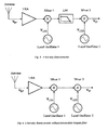
- The present invention is related to the reception or emission of radio-frequency signals by means of electronics circuits. Most modem radio-frequency signal receivers (abbreviated as RF receivers), contain a mixer means, to convert the radio-frequency (RF) signal to a lower-frequency signal. The principle schematic of such a RF receiver is depicted in Fig. 1. In most receivers, the electromagnetic signal, received by the antenna, is amplified first by a so-called "Low-Noise Amplifier (LNA)". Then, the signal is multiplied by a local-oscillator signal (ideally a sinusoidal signal) in a multiplying device called "mixer".
If we denote the received RF signal as A RF .cos(ω RF .t) (*) and the Local Oscillator signal as A LO . cos(ωLO .t), then the mixer output signal is given by: - In practice, only the second term of (1) is of interest. Hence, the RF input spectrum is shifted from a frequency ωRF to (ωRF-ωLO) (see Fig. 2). The RF signal is transformed from a high RF frequency to a lower frequency, where the signals are easier to treat. This new frequency ((ωRF-ωLO) is called the "Intermediate Frequency (IF)".
- If IF is equal to zero, the receiver is called a "Zero-IF receiver"; otherwise, it is denoted as a "Superheterodyne receiver". This principle is well-known since more than 60 years. A mixer is sometimes also denoted as a "Frequency Downconverter" or briefly "downconverter".
A similar principle can be applied in a radio-frequency transmitter. There, the mixer is Upconverting the signal frequency from a lower value to a high RF-frequency.
In practice, it is sometimes not obvious to downconvert signal frequencies by more than a factor of 10. E.g. an RF input signal of 5 GHz can be downconverted in one step to a signal of 0.5 GHz. When the desired frequency at the output of the downconverter is even lower than this 0.5 GHz, two downconversion steps are sometimes used (see Fig. 3). In a first downconverter, the signal frequency is converted from ωRF to ωIF1 = (ωRF-ωLO1). In a second downconversion step, the signal frequency is further reduced to ωIF2 = (ωIF1-ωLO2) = (ωRF-ωLO1-ωLO2). For practical reasons, it is often necessary to insert a lowpass filter in between the two downconverters, to eliminate unwanted signals at the output of the first downconverter. Such a circuit is e.g. described in the IEEE J. Solid-State Circuits, Dec. 2000, p. 1908
However, recent developments have shown that in some circumstances, this lowpass filter can be eliminated. The two-step downconverter architecture then reduces to the schematic of Fig. 4.
For sake of completeless, it should be pointed out that, in most practical applications, the Local oscillator signals are not sinusoidal signals, but square-wave signals. - The remaining drawbacks of the circuit of Fig. 4 are its complexity, linearity requirements and, as a result, relatively high power consumption. The invention described in this patent application provides a solution to improve these items.
- Although the explanation presented above is focussed on the reception of RF signals, it should be pointed out that mixers are also used for other applications, such as e.g. the emission of RF signals, wireline communications, optical fiber communications, speed detection systems etc. The invention is applicable also to these domains.
- The operation of the mixers in Fig. 4 can be described by means of the following mathematical equations:
These expressions can be re-written as:
The advantages of the circuit of Fig. 5 become more apparent when realising that, in most practical cases, the two local oscillator signals are (digital) square-wave signals. In this case, the second mixer of Fig. 5 reduces to a simple XOR gate circuit (either standard digital gate, ecl-gate or another kind of digital signal multiplier). This is shown in Fig. 6. The resulting circuit contains only one mixer. - In many applications, it is necessary to obtain two downconverter output signals with a 90 deg. Phase difference. These are called "quadrature signals". Such quadrature output signals can be obtained by modifying the circuit of Fig. 4 into the circuit of Fig. 7a. Now, two mixers are used for the second downconversion step. The different signals in this figure are given by:and


- In practice, only the last terms, with frequency (ω RF -ω LO1 - ω LO2) in (6a) and (6b) are important. As can be seen, these signals have a 90 degrees phase shift.
Again, the invention allows removing one mixer step in the signal path. - Another aspect of the invention is related to the re-configurable character of the schematics presented in Fig. 6 and Fig. 7: If the signal VLO1 Is replaced by a DC signal, all these drawings reduce to a standard single-step mixer architecture. In this way, a reconfigurable mixer architecture is obtained:
- When the signal VLO1 is a DC signal (or a digital "1" or "0"), a standard single-step mixer is obtained
- When the signal VLO1 is a Local Oscillator signal (sinusoidal, square wave or other), the schematics turn into two-step mixer circuits.
Claims (10)
- A means for deriving an output signal (denoted as VOUT) from an input signal (denoted as VRF) whereby frequency-domain components in the input signal cause frequency-domain components in the output signal, with frequencies that are equal to the input signal component's frequencies shifted by a given amount, characterised by a) the shift between input signal component's frequencies and output signal component's frequencies is equal to the sum of the frequencies of two other signals denoted as VLO1 (with frequency ωLO1) and VLO2 (with frequency ωLO2) respectively, and b) the signals VLO1 and VLO2 are combined by a signal combination means, to obtain a third signal (denoted as VLO3), and c) the input signal (VRF) information is not passing through said signal combination means.
- A means for deriving an output signal (denoted as VOUT) from an input signal (denoted as VRF) whereby frequency-domain components in the input signal cause frequency-domain components in the output signal, with frequencies that are equal to the input signal component's frequencies shifted by a given amount, characterised by a) the shift between input signal component's frequencies and output signal component's frequencies is equal to the difference of the frequencies of two other signals denoted as VLO1 (with frequency ωLO1) and VLO2 (with frequency ωLO2) respectively, and b) the signals VLO1 and VLO2 are combined by a signal combination means, to obtain a third signal (denoted as VLO3), and c) the input signal (VRF) information is not passing through said signal combination means.
- A means according to Claims 1 or 2, where VLO1 and/or VLO2 are signal harmonics of non-sinusoidal signals.
- A means according to one of the Claims 1 to 3, whereby the combined signal VLO3 has significant signal power at frequency ωLO1+ωLO2 and/or ωLO1-ωLO2.
- A means according to Claim 4 characterised in that said signal VLO3 is obtained by a signal multiplication of signals VLO1 and VLO2.
- A means according to Claim 1, 2, 3 or 4, where the two signals VLO1 and VLO2 are square-wave signals.
- A means according to Claim 5, where said signals VLO1 and VLO2.are square-wave signals, and where said multiplication device is performing an XOR function.
- A means according to one of the Claims 1 to 7, where VRF and VLO3 are combined by means of a multiplication device.
- A means according to one of the Claims 1 to 8, where only one signal multiplication means is present in the signal path between VRF and VOUT.
- A means for deriving two output signals (denoted as VOUT,I and VOUT,Q) from an input signal (denoted as VRF) whereby frequency-domain components in the input signal cause frequency-domain components in both output signals, with frequencies that are equal to the input signal component's frequencies shifted by a given amount, and where the phase of the signal component in VOUT,I differs by 90 degrees from the phase of the signal component in vOUT,Q. This means is further characterised by a) it contains two means according to one of the Claims 1 to 9, and b) these two means have a common signal VRF and c) either VLO1 or VLO2 are common to these two means.
Priority Applications (1)
| Application Number | Priority Date | Filing Date | Title |
|---|---|---|---|
| EP04447093A EP1585227A1 (en) | 2004-04-08 | 2004-04-08 | A two-step frequency converter with only one mixer in the signal path |
Applications Claiming Priority (1)
| Application Number | Priority Date | Filing Date | Title |
|---|---|---|---|
| EP04447093A EP1585227A1 (en) | 2004-04-08 | 2004-04-08 | A two-step frequency converter with only one mixer in the signal path |
Publications (1)
| Publication Number | Publication Date |
|---|---|
| EP1585227A1 true EP1585227A1 (en) | 2005-10-12 |
Family
ID=34896197
Family Applications (1)
| Application Number | Title | Priority Date | Filing Date |
|---|---|---|---|
| EP04447093A Withdrawn EP1585227A1 (en) | 2004-04-08 | 2004-04-08 | A two-step frequency converter with only one mixer in the signal path |
Country Status (1)
| Country | Link |
|---|---|
| EP (1) | EP1585227A1 (en) |
Citations (4)
| Publication number | Priority date | Publication date | Assignee | Title |
|---|---|---|---|---|
| GB622838A (en) * | 1943-05-25 | 1949-05-09 | Philips Nv | Improvements in or relating to tunable apparatus |
| US6085075A (en) * | 1997-12-05 | 2000-07-04 | U.S. Philips Corporation | Communication system, a communication device and a frequency synthesizer |
| US20030119470A1 (en) * | 2001-12-21 | 2003-06-26 | Persico Charles J. | Generating local oscillator signals for downconversion |
| US20040014446A1 (en) * | 2002-05-08 | 2004-01-22 | Sudipto Chakraborty | Methods and systems for odd-order LO compensation for even-harmonic mixers |
-
2004
- 2004-04-08 EP EP04447093A patent/EP1585227A1/en not_active Withdrawn
Patent Citations (4)
| Publication number | Priority date | Publication date | Assignee | Title |
|---|---|---|---|---|
| GB622838A (en) * | 1943-05-25 | 1949-05-09 | Philips Nv | Improvements in or relating to tunable apparatus |
| US6085075A (en) * | 1997-12-05 | 2000-07-04 | U.S. Philips Corporation | Communication system, a communication device and a frequency synthesizer |
| US20030119470A1 (en) * | 2001-12-21 | 2003-06-26 | Persico Charles J. | Generating local oscillator signals for downconversion |
| US20040014446A1 (en) * | 2002-05-08 | 2004-01-22 | Sudipto Chakraborty | Methods and systems for odd-order LO compensation for even-harmonic mixers |
Similar Documents
| Publication | Publication Date | Title |
|---|---|---|
| CN100431261C (en) | Improved mixer with multiple local oscillators and systems based thereon | |
| US20090286499A1 (en) | High dynamic range receiver | |
| US7046979B2 (en) | Receiver for rejecting image signal | |
| CN101395810B (en) | Apparatus with noise reduction for receiving and/or sending radiofrequency signals | |
| CN101588161A (en) | Filter circuit, wireless transmitter, and wireless receiver | |
| CN102707298B (en) | Receiver and communication signal receiving method | |
| KR100404772B1 (en) | Direct conversion receiver and transceiver | |
| US7085548B1 (en) | Harmonic mixer | |
| JP2006526913A (en) | Low power consumption receiver front end and devices based thereon | |
| US7450919B1 (en) | I/Q mismatch correction using transmitter leakage and gain modulation | |
| EP1585227A1 (en) | A two-step frequency converter with only one mixer in the signal path | |
| CN101350629B (en) | Prediction Method of Potential Disturbed Frequency Bands in Receiver RF System | |
| US6745020B2 (en) | Direct downconversion receiver | |
| US11500060B2 (en) | Radar receiver and method for receiving a radar signal | |
| US7302011B1 (en) | Quadrature frequency doubling system | |
| KR102100733B1 (en) | Apparatus and method for removing DC offset in Radar transceiver | |
| KR101233763B1 (en) | Wideband phase shift device | |
| US7991372B2 (en) | Receiver and electronic apparatus using the same | |
| JP2002111526A (en) | High-frequency ic circuit | |
| US7848728B2 (en) | Broadband balanced frequency converter | |
| JPH08107315A (en) | Frequency converter | |
| Passos et al. | RF Receiver Architectures | |
| US20030190901A1 (en) | Direct conversion receiving unit | |
| US20060284686A1 (en) | Quadrature phase oscillator using complex coefficient filter | |
| Kellerman | Modular approach to the development of a two-way radio receiver system |
Legal Events
| Date | Code | Title | Description |
|---|---|---|---|
| PUAI | Public reference made under article 153(3) epc to a published international application that has entered the european phase |
Free format text: ORIGINAL CODE: 0009012 |
|
| AK | Designated contracting states |
Kind code of ref document: A1 Designated state(s): AT BE BG CH CY CZ DE DK EE ES FI FR GB GR HU IE IT LI LU MC NL PL PT RO SE SI SK TR |
|
| AX | Request for extension of the european patent |
Extension state: AL HR LT LV MK |
|
| AKX | Designation fees paid | ||
| REG | Reference to a national code |
Ref country code: DE Ref legal event code: 8566 |
|
| STAA | Information on the status of an ep patent application or granted ep patent |
Free format text: STATUS: THE APPLICATION IS DEEMED TO BE WITHDRAWN |
|
| 18D | Application deemed to be withdrawn |
Effective date: 20060413 |