EP1585176A1 - Ferroelectric capacitor and method for fabricating the same - Google Patents
Ferroelectric capacitor and method for fabricating the same Download PDFInfo
- Publication number
- EP1585176A1 EP1585176A1 EP03701774A EP03701774A EP1585176A1 EP 1585176 A1 EP1585176 A1 EP 1585176A1 EP 03701774 A EP03701774 A EP 03701774A EP 03701774 A EP03701774 A EP 03701774A EP 1585176 A1 EP1585176 A1 EP 1585176A1
- Authority
- EP
- European Patent Office
- Prior art keywords
- ferroelectric
- layer
- bottom electrode
- component elements
- set forth
- Prior art date
- Legal status (The legal status is an assumption and is not a legal conclusion. Google has not performed a legal analysis and makes no representation as to the accuracy of the status listed.)
- Withdrawn
Links
Images




Classifications
-
- H—ELECTRICITY
- H10—SEMICONDUCTOR DEVICES; ELECTRIC SOLID-STATE DEVICES NOT OTHERWISE PROVIDED FOR
- H10D—INORGANIC ELECTRIC SEMICONDUCTOR DEVICES
- H10D1/00—Resistors, capacitors or inductors
- H10D1/60—Capacitors
- H10D1/68—Capacitors having no potential barriers
- H10D1/692—Electrodes
- H10D1/694—Electrodes comprising noble metals or noble metal oxides
-
- H—ELECTRICITY
- H10—SEMICONDUCTOR DEVICES; ELECTRIC SOLID-STATE DEVICES NOT OTHERWISE PROVIDED FOR
- H10D—INORGANIC ELECTRIC SEMICONDUCTOR DEVICES
- H10D1/00—Resistors, capacitors or inductors
- H10D1/60—Capacitors
- H10D1/68—Capacitors having no potential barriers
- H10D1/682—Capacitors having no potential barriers having dielectrics comprising perovskite structures
-
- H—ELECTRICITY
- H10—SEMICONDUCTOR DEVICES; ELECTRIC SOLID-STATE DEVICES NOT OTHERWISE PROVIDED FOR
- H10D—INORGANIC ELECTRIC SEMICONDUCTOR DEVICES
- H10D1/00—Resistors, capacitors or inductors
- H10D1/60—Capacitors
- H10D1/68—Capacitors having no potential barriers
- H10D1/692—Electrodes
- H10D1/696—Electrodes comprising multiple layers, e.g. comprising a barrier layer and a metal layer
Definitions
- the present invention relates to a ferroelectric capacitor used mainly for a nonvolatile memory device and a method of production of the same.
- PZT Pb (Zr x Ti 1-x ) O 3
- PZT is a perovskite crystal structural material having ferroelectric properties and electrooptic properties and is used for nonvolatile memory devices, electrooptic devices, etc. having large spontaneous polarization.
- ferroelectric thin films have been formed by various film-forming methods.
- thin film forming technologies are divided into physical vapor deposition (PVD) technologies and chemical processing technologies.
- PVD physical vapor deposition
- the PVD technologies used for forming ferroelectric thin films include electron beam vapor deposition, sputtering, laser ablation, etc.
- Chemical processing technologies include chemical solution deposition (CSD) and chemical vapor deposition (CVD).
- the PVD technologies mainly have the advantages that they can form films by a low pressure of 10 -5 Pa or less, give high purity and high cleanness, and give compatibility with semiconductor integrated circuit technologies, but have the defects of a low deposition speed, difficulty in control of the stoichiometric composition, high temperature annealing after deposition, etc.
- CSD has the advantages of uniformity of molecules, a high deposition speed, reproducibility of composition, ease of introduction of a dopant, etc., but has the problems of the heat treatment after deposition causing the film to crack, the absence of use of a vacuum tank, so the occasional intermixture of impurities, a change in the composition necessitating a change in the starting materials, etc.
- MOCVD metal organic chemical vapor deposition
- the present invention has as its object to solve the problems of the prior art explained above and provide a ferroelectric capacitor formed so that the morphology is good and the ferroelectric has a dominant axis of orientation.
- the present invention solves the above problem and provides a ferroelectric capacitor including a bottom electrode layer, a ferroelectric layer on the bottom electrode layer, and a top electrode layer on the ferroelectric layer, in which a ferroelectric is formed on the bottom electrode layer so as to have a dominant axis of orientation, the bottom electrode layer has a multilayer structure, and the layers of the bottom electrode have larger coefficients of diffusion of component elements of the ferroelectric or compounds comprised of the component elements to the bottom electrode the closer the layers to the ferroelectric layer.
- the ferroelectric capacitor according to the present invention can be produced by a method including a step of forming a ferroelectric layer by metal organic chemical vapor deposition and heating a substrate when forming this ferroelectric layer and a step of passing organometallic precursor including at least one type of the component elements of the ferroelectric layer to form the ferroelectric layer on the bottom electrode and form the component elements of the first layer of the bottom electrode contiguous with the ferroelectric layer and the component elements of the ferroelectric layer into an alloy or compound.
- the present invention by employing a configuration where the mismatch between the materials forming the first layer of the bottom electrode contiguous with the ferroelectric layer and the materials forming the ferroelectric layer becomes smaller, it is possible to obtain a ferroelectric capacitor formed so that the ferroelectric layer has a dominant axis of orientation.
- the ferroelectric capacitor according to the present invention may satisfy n i >n i+1 when the concentrations of the component elements of the ferroelectric or compounds comprised of the component elements in the i-th and i+1st layers of the bottom electrode counted from the ferroelectric layer side are n i and n i+1 .
- the first layer of the bottom electrode contiguous with the ferroelectric layer may be formed from an alloy or compound including the component elements of the ferroelectric.
- the ferroelectric layer includes Pb and Ti or Pb, Zr, and Ti as component elements.
- the ferroelectric layer includes Pb and Ti or Pb, Zr, and Ti as component elements and further includes at least type of element selected from the group comprised of La, Ca, Sr, and Nb.
- the ferroelectric layer is comprised of a ferroelectric including Pb and Ti or Pb, Zr, and Ti as component elements and a crystal orientation plane of (111).
- the ferroelectric layer is comprised of a ferroelectric including Pb and Ti or Pb, Zr, and Ti as component elements and a crystal orientation plane of (001).
- a thickness of the first layer of the bottom electrode contiguous with the ferroelectric layer is for example not more than 20 nm.
- the first layer of the bottom electrode contiguous with the ferroelectric layer for example includes Pt as a component element and a second layer of the bottom electrode contiguous with the first layer of the bottom electrode includes Ir as a component element.
- the ferroelectric layer is comprised of a perovskite ferroelectric including Pb
- the first layer of the bottom electrode is formed from a compound including Pb by passing organometallic precursor including Pb and a carrier gas and oxygenation gas right before forming the ferroelectric layer
- the ferroelectric layer is formed.
- the ferroelectric layer is comprised of a ferroelectric including Pb, Zr, and Ti as component elements
- Pb(THD) 2 is used as a Pb precursor
- Zr(DMHD) 4 is used as a Zr precursor
- Ti(iPrO) 2 (THD) 2 is used as a Ti precursor.
- the ferroelectric film By using a bottom electrode as explained above according to the present invention, it is possible form the ferroelectric film on the bottom electrode so as to have a dominant axis of orientation.
- a material having a strong self epitaxy and small lattice mismatch with thin film is sometimes used for the underlying layer.
- the thin film is made a two-layer structure with the first layer grown with crystal nuclei called an "initial layer” or “seed layer” and used as a nucleus to grow a thin film.
- an "initial layer” or “seed layer” is used as a nucleus to grow a thin film.
- PZT Pt having small lattice mismatch is often used.
- FIG. 1 shows a sectional SEM image of a PZT film grown on Pt.
- a reaction layer of Pt and Pb is observed at the boundary of the PZT and Pt. It is learned that due to the expansion of volume of the reaction layer of Pt and Pb, the morphology deteriorates.
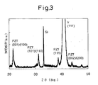
- FIG. 2 shows a sectional SEM image of the PZT film formed on the Ir. No reaction product is seen at the boundary between the PZT and Ir. A good boundary is formed. However, as shown in FIG. 3, the orientation becomes random orientation.
- a Pt layer smaller in thickness compared with Ir is deposited on the Ir and first a Pb precursor is supplied to form a PbPt alloy on the Ir.
- the Pb supplied on the Pt diffuses in the Pt to react with it, but the reaction between Ir and Pb is lower compared with Pt, diffusion of Pb at the Pt-Ir boundary is suppressed, and the Pb diffuses uniformly in the Pt layer in the horizontal direction with respect to the substrate. Due to this, a uniform PtPb alloy is formed on the Ir. Further, since the thickness of the Pt is small and the Pb is further uniformly diffused, no local expansion occurs. This PtPb alloy has a smaller lattice mismatch with PZT compared with Pt, so later PZT layer is affected by the orientation of PtPb and becomes remarkably oriented.
- a 6-inch Si (100) substrate was used as the substrate.
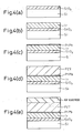
- the Si substrate was thermally oxidized to form a 100 nm thick SiO 2 layer (FIG. 4(a)).
- an Ir layer was formed to a thickness of 150 nm by sputtering (FIG. 4(b)).
- a Ti layer and TiO 2 layer may also be formed.
- a PtPb layer was deposited to a thickness of about 10 nm using a PtPb alloy target by sputtering (FIG. 4(c)).
- metal organic chemical vapor deposition was used.
- organometallic material Pb(THD) 2 [lead bis(tetramethylheptanedione)], Zr(DMHD) 4 [zirconium tetrakis(dimethylheptanedionate)], and Ti(iPrO) 2 (THD) 2 [titanium (diisopropoxy)bis(tetramethylheptanedione)] were used.
- THF tetrahydrofuran
- This liquid precursor was introduced into a vaporizer controlled in flow rate by a liquid mass flow controller and held at 260°C to convert it into a gas.
- the carrier gas N 2
- the gasified organometallic precursor and carrier gas were mixed with oxygen gas in a gas mixing chamber above a reaction chamber and the result passed through a shower head to be introduced to a CVD reaction chamber.
- the above obtained PbPt/Ir/SiO 2 /Si was used as the wafer.
- the wafer was placed on a susceptor at the top of the heating heater and was heated for 240 seconds so that the substrate temperature became a uniform 580°C.
- the pressure of the reaction chamber was adjusted so as to become 670 Pa in total pressure.
- the flow rate of the oxygen gas was made 2500 sccm. While heating the wafer, the material gas vaporized at the vaporizer was passed through an exhaust line and not sent to the CVD reaction chamber.
- the precursor gases was mixed with oxygen gas in the gas mixing chamber and the result passed through a shower head to be introduced into the reaction chamber.
- the precursors were adjusted to a ratio of 0.78 by Pb/(Zr+Ti) flow rate ratio and a ratio of 0.46 by Zr/(Zr+Ti) flow rate ratio.
- only the THF solvent was passed at a ratio of 1.33 by THF/(Pb+Zr+Ti) flow rate ratio and introduced into the vaporizer.
- the valve connecting the vaporizer to the exhaust line was closed and simultaneously the valve of the piping from the vaporizer to the gas mixing chamber was opened to introduce the solvent to the mixing chamber together with the carrier gas.
- oxygen gas was also introduced into the mixing chamber and mixed with the precursor gases.
- the gas mixed at the gas mixing chamber was sent through a shower head to a deposition chamber maintained at 670 Pa and a film was formed on the substrate to a thickness of 120 nm (FIG. 4(d)).
- the PZT film formed by the above method was strongly (111) oriented as shown in FIG. 5.
- the (111) orientation rate was at least 90%.
- an X-ray diffraction pattern of the case of directly forming PZT on IR is also shown. Further, as shown in FIG. 6, this has an amount of polarization of at least 60 ⁇ C/cm 2 by an applied voltage of 1.8V.
- a 6-inch Si (100) substrate was used as the substrate.
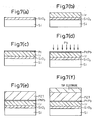
- the Si substrate was thermally oxidized to form a 100 nm thick SiO 2 layer (FIG. 7(a)).
- an Ir layer was formed to a thickness of 150 nm by sputtering (FIG. 7(b)).
- a Ti layer and TiO 2 layer may also be formed.
- a Pt layer was deposited to a thickness of about 10 nm by sputtering (FIG. 7(c)).
- metal organic chemical vapor deposition was used.
- organometallic materials Pb(DPM) 2 [lead bis(dipivaroylmethanate)], Zr(DMHD) 4 [zirconium tetrakis(dimethylheptanedionate)], and Ti(iPrO) 2 (DMP) 2 [titanium (diisopropoxy)bis(dipivaroylmethanate)] were used. These materials were dissolved in THF (tetrahydrofuran) solvent to a concentration of 0.3 mol/L. This liquid was used as a starting precursor.
- THF tetrahydrofuran
- This liquid precursor was introduced into a vaporizer controlled in flow rate by a liquid mass flow controller and held at 260°C to convert it into a gas.
- a carrier gas N 2
- the gasified organometallic precursor and carrier gas were mixed with oxygen gas in a gas mixing chamber above a reaction chamber and the result passed through a shower head to be introduced to a CVD reaction chamber.
- the above obtained Pt/Ir/SiO 2 /Si was used as the wafer.
- the wafer was placed on a susceptor at the top of the heating heater and was heated for 240 seconds so that the substrate temperature became a uniform 580°C.
- the pressure of the reaction chamber was adjusted so as to become 670 Pa in total pressure.
- the flow rate of the oxygen gas was made 2500 sccm. While heating the wafer, the material gas vaporized at the vaporizer was passed through an exhaust line and not sent to the CVD reaction chamber.
- the Pb(DPM) 2 /THF precursor was supplied on to the wafer at a flow rate of 0.2 to 0.5 ml/min for 10 to 30 seconds. Due to this, the Pt layer and Pb reacted and a PtPb layer was formed (FIG. 7(d)).
- the Zr and Ti precursors were supplied and the vaporized Pb, Zr, and Ti precursor gases were mixed with oxygen gas in a gas mixing chamber. The result was passed through a shower head to be introduced into the reaction chamber. The precursors were adjusted to a ratio of 0.78 by Pb/(Zr+Ti) flow rate ratio and a ratio of 0.46 by Zr/(Zr+Ti) flow rate ratio.
- THF solvent was passed at a ratio of 1.33 by THF/(Pb+Zr+Ti) flow rate ratio and introduced into the vaporizer.
- the valve connecting the vaporizer to the exhaust line was closed and simultaneously the valve of the piping from the vaporizer to the gas mixing chamber was opened to introduce the solvent to the mixing chamber together with the carrier gas.
- oxygen gas was also introduced into the mixing chamber and mixed with the precursor gases. The gas obtained by mixing at the gas mixing chamber was sent through a shower head to a deposition chamber maintained at 670 Pa and a film was formed on the substrate to a thickness of 120 nm (FIG. 7(e)).
- IrO x As a top electrode, IrO x was formed by sputtering to a thickness of about 100 nm to form a capacitor (FIG. 7(f)).
- the PZT film formed by the above method in the same way as the case of Example 1, was (111) oriented at least 90%.
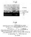
- a sectional SEM image of this PZT film is shown in FIG. 8.
- the Pt layer is thin, so no expansion of volume due to the reaction of Pt and Pb at the PZT/Pt boundary such as formed on a thick Pt (see FIG. 1) is seen and a good boundary state is obtained.
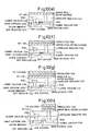
- FIG. 9 is a schematic sectional view of the structure of a semiconductor device according to this example, while FIG. 10 is a sectional process chart of the method of production of the semiconductor device.
- a silicon substrate is formed with a memory cell transistor having a gate electrode formed through a gate insulating film and source/drain diffusion layer formed on the silicon substrate at the two sides of the gate electrode.
- An interlayer insulating film is then formed on the silicon substrate formed with the memory cell transistor. Plugs electrically connected to the source/drain diffusion layer are buried in the interlayer insulating film. Bit lines electrically connected through the plugs to the source/drain diffusion layer are formed on the inter-layer insulating film.
- a further interlayer insulating film is formed on the interlayer insulating film formed with the bit lines. Plugs electrically connected to the source/drain diffusion layer are buried in the interlayer insulating film.
- a barrier metal and bottom electrode is formed on the interlayer insulating film in which the plugs are buried.
- Ir As the bottom electrode, Ir, then a PtPb layer or Pt layer are formed.
- a capacitor dielectric film comprised of a PZT film is formed on the bottom electrode.
- a top electrode comprised of Pt or Ir or IrO x is formed on the dielectric film. Due to this, a ferroelectric capacitor comprised of a bottom electrode, a capacitor dielectric film, and a top electrode is configured.
- a silicon substrate is for example formed with an element isolation film by the shallow trench method.
- a memory cell transistor having a gate electrode formed through the gate insulating film and source/drain diffusion regions formed on the silicon substrate at the two sides of the gate electrode is formed on an element region defined by an element isolation film in the same way as the usual method of formation of a MOS transistor (FIG. 10(a)).
- a silicon oxide film is deposited on the silicon substrate formed with the memory cell transistor by for example CVD so as to form an interlayer insulating film comprised of a silicon oxide film.
- the surface of the interlayer insulating film is polished by CMP (chemical mechanical polishing) to flatten the surface of the interlayer insulating film.
- a contact hole reaching the source/drain diffusion layer is formed in the interlayer insulating film by lithography technology and etching technology (FIG. 10(b)).
- a tungsten (W) film is deposited by sputtering, then this is polished by CMP until the surface of the interlayer insulating film is exposed. In this way, a plug electrically connected to the source/drain diffusion layer buried in the contact hole is formed.
- a W film is deposited by sputtering, then the W film is patterned by lithography technology and etching technology to form bit lines connected through the plug to the source/drain diffusion layer (FIG. 10(c)).
- a silicon oxide film is deposited by for example CVD on the interlayer insulating film formed with the bit lines to form an interlayer insulating film comprised of a silicon oxide film.
- a W film is deposited by sputtering, then this is polished by CMP until the surface of the interlayer insulating film is exposed. In this way, a plug electrically connected to the source/drain diffusion layer buried in the contact hole is formed.
- a barrier metal and bottom electrode comprised of Ir are formed to a thickness of 150 nm (FIG. 10(e)).
- Pb(DPM) 2 lead bis(dipivaroylmethanate)
- Zr(DMHD) 4 zirconium tetrakis(dimethylheptanedionate)]
- Ti(iPrO) 2 (DPM) 2 titanium (diisopropoxy)bis(dipivaroylmethanate)] were used.
- THF tetrahydrofuran
- the carrier gas (N 2 ) was simultaneously introduced into the vaporizer at a flow rate of 300 sccm.
- the gasified organometallic precursor and carrier gas were mixed with oxygen gas in a gas mixing chamber above a reaction chamber and the result passed through a shower head to be introduced to a CVD reaction chamber.
- the above obtained Pt/Ir/SiO 2 /Si was used as the wafer.
- the wafer was placed on a susceptor at the top of the heating heater and was heated for 240 seconds so that the substrate temperature became a uniform 580°C.
- the pressure of the reaction chamber was adjusted so as to become 670 Pa in total pressure.
- the flow rate of the oxygen gas was made 2500 sccm. While heating the wafer, the material gas vaporized at the vaporizer was passed through an exhaust line and not sent to the CVD reaction chamber.
- the Pb(DPM) 2 /THF precursor was supplied at a flow rate of 0.2 to 0.5 ml/min on to the wafer for 10 to 30 seconds. Due to this, the Pt layer and Pb reacted and a PtPb layer was formed. After this, the PZT film was formed. When using PtPb as the bottom electrode, this process is not performed.
- Pb, Zr, and Ti precursor gases were mixed with oxygen gas in the gas mixing chamber and the result was passed through a shower head to introduce it to a reaction chamber.
- the precursors were adjusted to a ratio of 0.78 by Pb/(Zr+Ti) flow rate ratio and to a ratio of 0.46 by Zr/(Zr+Ti) flow rate ratio.
- Only the THF solvent was passed at a ratio of 1.33 by THF/(Pb+Zr+Ti) flow rate ratio and introduced to a vaporizer.
- the valve connecting the exhaust line from the vaporizer was closed, at the same time the valve of the piping from the vaporizer to the gas mixing chamber was opened, and the vapor was introduced to the mixing chamber along with the carrier gas.
- the oxygen gas was also introduced into the mixing chamber and mixed with the precursor gases.
- the gas mixed in the gas mixing chamber was passed through a shower head and sent to a deposition chamber maintained at 670 Pa, and a film was formed until 120 nm thickness on the substrate (FIG. 10(f)).
Landscapes
- Semiconductor Memories (AREA)
- Fixed Capacitors And Capacitor Manufacturing Machines (AREA)
- Semiconductor Integrated Circuits (AREA)
- Formation Of Insulating Films (AREA)
Abstract
A ferroelectric capacitor including a bottom
electrode layer, a ferroelectric layer on the bottom
electrode layer, and a top electrode layer on the
ferroelectric layer, in which a ferroelectric is formed
on the bottom electrode layer so as to have a dominant
axis of orientation, the bottom electrode layer has a
multilayer structure, and the layers of the bottom
electrode have larger coefficients of diffusion of
component elements of the ferroelectric or compounds
comprised of the component elements to the bottom
electrode the closer the layers to the ferroelectric
layer. This is produced by a method including a step of
forming a ferroelectric layer by metal organic chemical
vapor deposition and heating a substrate when forming
this ferroelectric layer and a step of passing
organometallic precursor including at least one type of
the component elements of the ferroelectric layer to form
the ferroelectric layer on the bottom electrode and form
the component elements of the first layer of the bottom
electrode contiguous with the ferroelectric layer and the
component elements of the ferroelectric layer into an
alloy or compound. A ferroelectric capacitor formed so
that the morphology is good and the ferroelectric has a
dominant axis of orientation is obtained.
Description
The present invention relates to a ferroelectric
capacitor used mainly for a nonvolatile memory device and
a method of production of the same.
PZT [Pb (ZrxTi1-x) O3] is a perovskite crystal
structural material having ferroelectric properties and
electrooptic properties and is used for nonvolatile
memory devices, electrooptic devices, etc. having large
spontaneous polarization.
Up until now, ferroelectric thin films have been
formed by various film-forming methods. In general, thin
film forming technologies are divided into physical vapor
deposition (PVD) technologies and chemical processing
technologies.
The PVD technologies used for forming ferroelectric
thin films include electron beam vapor deposition,
sputtering, laser ablation, etc. Chemical processing
technologies include chemical solution deposition (CSD)
and chemical vapor deposition (CVD).
The PVD technologies mainly have the advantages that
they can form films by a low pressure of 10-5 Pa or less,
give high purity and high cleanness, and give
compatibility with semiconductor integrated circuit
technologies, but have the defects of a low deposition
speed, difficulty in control of the stoichiometric
composition, high temperature annealing after deposition,
etc.
CSD has the advantages of uniformity of molecules, a
high deposition speed, reproducibility of composition,
ease of introduction of a dopant, etc., but has the
problems of the heat treatment after deposition causing
the film to crack, the absence of use of a vacuum tank,
so the occasional intermixture of impurities, a change in
the composition necessitating a change in the starting
materials, etc.
Among the above art, for the formation of
ferroelectric thin film, metal organic chemical vapor
deposition (MOCVD) is the most promising. MOCVD has the
advantages of superior film uniformity and composition
control, high film density, high deposition speed,
superior step coverage, etc. In particular, the step
coverage obtained by MOCVD is not obtainable by any other
method. Further, the composition of the film, for
example, the PZT, can be easily changed using the same
materials by the flow rates of the materials.
Many of the reports of MOCVD relating to the
formation of ferroelectric thin film use the bubbling
method of bubbling liquid materials by a gas and sending
them to a reaction chamber by a carrier gas, but the low
film formation speed is a problem (for example, see
Japanese Unexamined Patent Publication (Kokai) No. 5-17286).
Further, the only Pb liquid material used when
forming PZT is a tetraethyl lead-based toxic material.
This is a problem. From the viewpoint of using nontoxic
materials, there is sublimation for making solid organic
materials sublimate and sending them to a reaction
chamber, but this method is poor in reproducibility of
the composition, film thickness, etc. (for example, see
Japanese Unexamined Patent Publication (Kokai) No. 2002-319581)
.
Recently, solution vaporized metal organic chemical
vapor deposition for dissolving liquid organic materials
or solid organic materials etc. in an organic solvent to
obtain a precursor, vaporizing the liquid precursor by a
vaporizer, and introducing the result into the reaction
chamber to form a thin film has been researched. This
method is considered promising in that it has the
possibility of a good reproducibility and high film
forming speed, but there are almost no reports indicating
that a ferroelectric thin film having a high
crystallinity and orientation is obtained. Almost all are
non-oriented films or (100) oriented. There are virtually
no reports of obtaining (111) orientation enabling
utilization of the polarization of all crystal grains.
When using Pt for the bottom electrode as is the
frequent practice with ferroelectric capacitors, there is
the method of depositing an amorphous layer by sputtering
or the sol-gel method, then using rapid heat treatment to
orient the ferroelectric utilizing the strong self
epitaxy of the (111) plane of Pt. However, in the case of
for example metal organic deposition for heating the
substrate and depositing and crystallizing the thin film,
there was the problem for example that in PZT, the Pb
would conspicuously diffuse to the bottom electrode side
to form an alloy with the Pt and cause expansion of
volume and thereby remarkably degrade the morphology.
When using Ir for the bottom electrode, since the
reactivity with Pb is lower than Pt, no reaction layer is
formed and the morphology is relatively good. However,
compared with Pt, the self epitaxy is weak and the
lattice mismatch with PZT is greater than Pt. Due to
there, there was the problem of difficult orientation of
the ferroelectric.
The present invention has as its object to solve the
problems of the prior art explained above and provide a
ferroelectric capacitor formed so that the morphology is
good and the ferroelectric has a dominant axis of
orientation.
The present invention solves the above problem and
provides a ferroelectric capacitor including a bottom
electrode layer, a ferroelectric layer on the bottom
electrode layer, and a top electrode layer on the
ferroelectric layer, in which a ferroelectric is formed
on the bottom electrode layer so as to have a dominant
axis of orientation, the bottom electrode layer has a
multilayer structure, and the layers of the bottom
electrode have larger coefficients of diffusion of
component elements of the ferroelectric or compounds
comprised of the component elements to the bottom
electrode the closer the layers to the ferroelectric
layer.
The ferroelectric capacitor according to the present
invention can be produced by a method including a step of
forming a ferroelectric layer by metal organic chemical
vapor deposition and heating a substrate when forming
this ferroelectric layer and a step of passing
organometallic precursor including at least one type of
the component elements of the ferroelectric layer to form
the ferroelectric layer on the bottom electrode and form
the component elements of the first layer of the bottom
electrode contiguous with the ferroelectric layer and the
component elements of the ferroelectric layer into an
alloy or compound.
In the present invention, by employing a
configuration where the mismatch between the materials
forming the first layer of the bottom electrode
contiguous with the ferroelectric layer and the materials
forming the ferroelectric layer becomes smaller, it is
possible to obtain a ferroelectric capacitor formed so
that the ferroelectric layer has a dominant axis of
orientation.
In a preferred aspect, the ferroelectric capacitor
according to the present invention may satisfy ni>ni+1 when
the concentrations of the component elements of the
ferroelectric or compounds comprised of the component
elements in the i-th and i+1st layers of the bottom
electrode counted from the ferroelectric layer side are ni
and ni+1. Further, the first layer of the bottom electrode
contiguous with the ferroelectric layer may be formed
from an alloy or compound including the component
elements of the ferroelectric.
The ferroelectric layer includes Pb and Ti or Pb,
Zr, and Ti as component elements. Alternatively, the
ferroelectric layer includes Pb and Ti or Pb, Zr, and Ti
as component elements and further includes at least type
of element selected from the group comprised of La, Ca,
Sr, and Nb.
The ferroelectric layer is comprised of a
ferroelectric including Pb and Ti or Pb, Zr, and Ti as
component elements and a crystal orientation plane of
(111). Alternatively, the ferroelectric layer is
comprised of a ferroelectric including Pb and Ti or Pb,
Zr, and Ti as component elements and a crystal
orientation plane of (001).
A thickness of the first layer of the bottom
electrode contiguous with the ferroelectric layer is for
example not more than 20 nm. The first layer of the
bottom electrode contiguous with the ferroelectric layer
for example includes Pt as a component element and a
second layer of the bottom electrode contiguous with the
first layer of the bottom electrode includes Ir as a
component element.
In a preferred aspect of the method for producing a
ferroelectric capacitor according to the present
invention, the ferroelectric layer is comprised of a
perovskite ferroelectric including Pb, the first layer of
the bottom electrode is formed from a compound including
Pb by passing organometallic precursor including Pb and a
carrier gas and oxygenation gas right before forming the
ferroelectric layer, then the ferroelectric layer is
formed. Alternatively, the ferroelectric layer is
comprised of a ferroelectric including Pb, Zr, and Ti as
component elements, Pb(THD)2 is used as a Pb precursor,
Zr(DMHD)4 is used as a Zr precursor, and Ti(iPrO)2(THD)2
is used as a Ti precursor.
By using a bottom electrode as explained above
according to the present invention, it is possible form
the ferroelectric film on the bottom electrode so as to
have a dominant axis of orientation.
In general, when orienting a thin film, a material
having a strong self epitaxy and small lattice mismatch
with thin film is sometimes used for the underlying
layer. Further, sometimes the thin film is made a two-layer
structure with the first layer grown with crystal
nuclei called an "initial layer" or "seed layer" and used
as a nucleus to grow a thin film. However, in the latter
case, when considering the mass production of thin film,
increased complexity of the process or control of
parameters at the time of thin film growth become
difficult. It is desirable to simplify the process as
much as possible. For example, in the case of PZT, Pt
having small lattice mismatch is often used.
FIG. 1 shows a sectional SEM image of a PZT film
grown on Pt. A reaction layer of Pt and Pb is observed at
the boundary of the PZT and Pt. It is learned that due to
the expansion of volume of the reaction layer of Pt and
Pb, the morphology deteriorates. FIG. 2 shows a sectional
SEM image of the PZT film formed on the Ir. No reaction
product is seen at the boundary between the PZT and Ir. A
good boundary is formed. However, as shown in FIG. 3, the
orientation becomes random orientation.
Therefore, a Pt layer smaller in thickness compared
with Ir is deposited on the Ir and first a Pb precursor
is supplied to form a PbPt alloy on the Ir. The Pb
supplied on the Pt diffuses in the Pt to react with it,
but the reaction between Ir and Pb is lower compared with
Pt, diffusion of Pb at the Pt-Ir boundary is suppressed,
and the Pb diffuses uniformly in the Pt layer in the
horizontal direction with respect to the substrate. Due
to this, a uniform PtPb alloy is formed on the Ir.
Further, since the thickness of the Pt is small and the
Pb is further uniformly diffused, no local expansion
occurs. This PtPb alloy has a smaller lattice mismatch
with PZT compared with Pt, so later PZT layer is affected
by the orientation of PtPb and becomes remarkably
oriented.
Below, the present invention will be explained
further by examples. However, the present invention is
not limited by these examples in any way.
As the substrate, a 6-inch Si (100) substrate was
used. The Si substrate was thermally oxidized to form a
100 nm thick SiO2 layer (FIG. 4(a)). On top of this, an Ir
layer was formed to a thickness of 150 nm by sputtering
(FIG. 4(b)). As the bonding layer between the SiO2 and Ir,
a Ti layer and TiO2 layer may also be formed. On the Ir
layer, a PtPb layer was deposited to a thickness of about
10 nm using a PtPb alloy target by sputtering (FIG.
4(c)).
Next, the process of formation of a PZT film will be
explained.
For forming a PZT film, metal organic chemical vapor
deposition was used. As the organometallic material,
Pb(THD)2 [lead bis(tetramethylheptanedione)], Zr(DMHD)4
[zirconium tetrakis(dimethylheptanedionate)], and
Ti(iPrO)2(THD)2 [titanium
(diisopropoxy)bis(tetramethylheptanedione)] were used.
These materials were dissolved in THF (tetrahydrofuran)
solvent to a concentration of 0.3 mol/L. This liquid was
used as a starting precursor. This liquid precursor was
introduced into a vaporizer controlled in flow rate by a
liquid mass flow controller and held at 260°C to convert
it into a gas. At this time, the carrier gas (N2) was
simultaneously introduced into the vaporizer at a flow
rate of 300 sccm. The gasified organometallic precursor
and carrier gas were mixed with oxygen gas in a gas
mixing chamber above a reaction chamber and the result
passed through a shower head to be introduced to a CVD
reaction chamber.
As the wafer, the above obtained PbPt/Ir/SiO2/Si was
used. The wafer was placed on a susceptor at the top of
the heating heater and was heated for 240 seconds so that
the substrate temperature became a uniform 580°C. The
pressure of the reaction chamber was adjusted so as to
become 670 Pa in total pressure. The flow rate of the
oxygen gas was made 2500 sccm. While heating the wafer,
the material gas vaporized at the vaporizer was passed
through an exhaust line and not sent to the CVD reaction
chamber.
After heating the wafer, the precursor gases was
mixed with oxygen gas in the gas mixing chamber and the
result passed through a shower head to be introduced into
the reaction chamber. The precursors were adjusted to a
ratio of 0.78 by Pb/(Zr+Ti) flow rate ratio and a ratio
of 0.46 by Zr/(Zr+Ti) flow rate ratio. Further, only the
THF solvent was passed at a ratio of 1.33 by
THF/(Pb+Zr+Ti) flow rate ratio and introduced into the
vaporizer. After the substrate heating step, the valve
connecting the vaporizer to the exhaust line was closed
and simultaneously the valve of the piping from the
vaporizer to the gas mixing chamber was opened to
introduce the solvent to the mixing chamber together with
the carrier gas. On the other hand, oxygen gas was also
introduced into the mixing chamber and mixed with the
precursor gases. The gas mixed at the gas mixing chamber
was sent through a shower head to a deposition chamber
maintained at 670 Pa and a film was formed on the
substrate to a thickness of 120 nm (FIG. 4(d)).
Next, a top electrode of Pt, Ir, IrOx, etc. was
formed on the PZT film (FIG. 4(e)).
The PZT film formed by the above method was strongly
(111) oriented as shown in FIG. 5. The (111) orientation
rate was at least 90%. As reference, an X-ray diffraction
pattern of the case of directly forming PZT on IR is also
shown. Further, as shown in FIG. 6, this has an amount of
polarization of at least 60 µC/cm2 by an applied voltage
of 1.8V.
As the substrate, a 6-inch Si (100) substrate was
used. The Si substrate was thermally oxidized to form a
100 nm thick SiO2 layer (FIG. 7(a)). On top of this, an Ir
layer was formed to a thickness of 150 nm by sputtering
(FIG. 7(b)). As the bonding layer between the SiO2 and Ir,
a Ti layer and TiO2 layer may also be formed. On the Ir
layer, a Pt layer was deposited to a thickness of about
10 nm by sputtering (FIG. 7(c)).
Next, the process of forming a PZT film will be
explained.
For forming a PZT film, metal organic chemical vapor
deposition was used. As the organometallic materials,
Pb(DPM)2 [lead bis(dipivaroylmethanate)], Zr(DMHD)4
[zirconium tetrakis(dimethylheptanedionate)], and
Ti(iPrO)2(DMP)2 [titanium
(diisopropoxy)bis(dipivaroylmethanate)] were used. These
materials were dissolved in THF (tetrahydrofuran) solvent
to a concentration of 0.3 mol/L. This liquid was used as
a starting precursor. This liquid precursor was
introduced into a vaporizer controlled in flow rate by a
liquid mass flow controller and held at 260°C to convert
it into a gas. At this time, a carrier gas (N2) was
simultaneously introduced into the vaporizer at a flow
rate of 300 sccm. The gasified organometallic precursor
and carrier gas were mixed with oxygen gas in a gas
mixing chamber above a reaction chamber and the result
passed through a shower head to be introduced to a CVD
reaction chamber.
As the wafer, the above obtained Pt/Ir/SiO2/Si was
used. The wafer was placed on a susceptor at the top of
the heating heater and was heated for 240 seconds so that
the substrate temperature became a uniform 580°C. The
pressure of the reaction chamber was adjusted so as to
become 670 Pa in total pressure. The flow rate of the
oxygen gas was made 2500 sccm. While heating the wafer,
the material gas vaporized at the vaporizer was passed
through an exhaust line and not sent to the CVD reaction
chamber.
After heating the wafer, first only the Pb(DPM)2/THF
precursor was supplied on to the wafer at a flow rate of
0.2 to 0.5 ml/min for 10 to 30 seconds. Due to this, the
Pt layer and Pb reacted and a PtPb layer was formed (FIG.
7(d)). After this, the Zr and Ti precursors were supplied
and the vaporized Pb, Zr, and Ti precursor gases were
mixed with oxygen gas in a gas mixing chamber. The result
was passed through a shower head to be introduced into
the reaction chamber. The precursors were adjusted to a
ratio of 0.78 by Pb/(Zr+Ti) flow rate ratio and a ratio
of 0.46 by Zr/(Zr+Ti) flow rate ratio. Further, only the
THF solvent was passed at a ratio of 1.33 by
THF/(Pb+Zr+Ti) flow rate ratio and introduced into the
vaporizer. After the substrate heating step, the valve
connecting the vaporizer to the exhaust line was closed
and simultaneously the valve of the piping from the
vaporizer to the gas mixing chamber was opened to
introduce the solvent to the mixing chamber together with
the carrier gas. On the other hand, oxygen gas was also
introduced into the mixing chamber and mixed with the
precursor gases. The gas obtained by mixing at the gas
mixing chamber was sent through a shower head to a
deposition chamber maintained at 670 Pa and a film was
formed on the substrate to a thickness of 120 nm (FIG.
7(e)).
As a top electrode, IrOx was formed by sputtering to
a thickness of about 100 nm to form a capacitor (FIG.
7(f)).
The PZT film formed by the above method, in the same
way as the case of Example 1, was (111) oriented at least
90%. A sectional SEM image of this PZT film is shown in
FIG. 8. In this structure, the Pt layer is thin, so no
expansion of volume due to the reaction of Pt and Pb at
the PZT/Pt boundary such as formed on a thick Pt (see
FIG. 1) is seen and a good boundary state is obtained.
Here, the actual process of forming a ferroelectric
capacitor on a semiconductor circuit board will be
explained.
FIG. 9 is a schematic sectional view of the
structure of a semiconductor device according to this
example, while FIG. 10 is a sectional process chart of
the method of production of the semiconductor device.
First, the structure of the semiconductor device
will be explained using FIG. 9.
A silicon substrate is formed with a memory cell
transistor having a gate electrode formed through a gate
insulating film and source/drain diffusion layer formed
on the silicon substrate at the two sides of the gate
electrode. An interlayer insulating film is then formed
on the silicon substrate formed with the memory cell
transistor. Plugs electrically connected to the
source/drain diffusion layer are buried in the interlayer
insulating film. Bit lines electrically connected through
the plugs to the source/drain diffusion layer are formed
on the inter-layer insulating film. A further interlayer
insulating film is formed on the interlayer insulating
film formed with the bit lines. Plugs electrically
connected to the source/drain diffusion layer are buried
in the interlayer insulating film.
A barrier metal and bottom electrode is formed on
the interlayer insulating film in which the plugs are
buried. When using Ir as the bottom electrode, Ir, then a
PtPb layer or Pt layer are formed. A capacitor dielectric
film comprised of a PZT film is formed on the bottom
electrode. A top electrode comprised of Pt or Ir or IrOx
is formed on the dielectric film. Due to this, a
ferroelectric capacitor comprised of a bottom electrode,
a capacitor dielectric film, and a top electrode is
configured.
Next, the method of production of a semiconductor
device will be explained using FIG. 10.
First, a silicon substrate is for example formed
with an element isolation film by the shallow trench
method. Next, a memory cell transistor having a gate
electrode formed through the gate insulating film and
source/drain diffusion regions formed on the silicon
substrate at the two sides of the gate electrode is
formed on an element region defined by an element
isolation film in the same way as the usual method of
formation of a MOS transistor (FIG. 10(a)).
Next, a silicon oxide film is deposited on the
silicon substrate formed with the memory cell transistor
by for example CVD so as to form an interlayer insulating
film comprised of a silicon oxide film.
Next, for example, the surface of the interlayer
insulating film is polished by CMP (chemical mechanical
polishing) to flatten the surface of the interlayer
insulating film.
Next, a contact hole reaching the source/drain
diffusion layer is formed in the interlayer insulating
film by lithography technology and etching technology
(FIG. 10(b)).
Next, for example, a tungsten (W) film is deposited
by sputtering, then this is polished by CMP until the
surface of the interlayer insulating film is exposed. In
this way, a plug electrically connected to the
source/drain diffusion layer buried in the contact hole
is formed.
Next, for example, a W film is deposited by
sputtering, then the W film is patterned by lithography
technology and etching technology to form bit lines
connected through the plug to the source/drain diffusion
layer (FIG. 10(c)).
Next, a silicon oxide film is deposited by for
example CVD on the interlayer insulating film formed with
the bit lines to form an interlayer insulating film
comprised of a silicon oxide film.
Next, a contact hole reaching the source/diffusion
layer is formed in the interlayer insulating film by
lithography technology and etching technology (FIG.
10(d)).
Next, for example, a W film is deposited by
sputtering, then this is polished by CMP until the
surface of the interlayer insulating film is exposed. In
this way, a plug electrically connected to the
source/drain diffusion layer buried in the contact hole
is formed.
Next, a barrier metal and bottom electrode comprised
of Ir are formed to a thickness of 150 nm (FIG. 10(e)).
Next, the process of formation of PZT will be
explained.
As the organometallic material, Pb(DPM)2 [lead
bis(dipivaroylmethanate)], Zr(DMHD)4 [zirconium
tetrakis(dimethylheptanedionate)], and Ti(iPrO)2(DPM)2
[titanium (diisopropoxy)bis(dipivaroylmethanate)] were
used. These materials were dissolved in THF
(tetrahydrofuran) solvent to a concentration of 0.3
mol/L. This liquid was used as a starting precursor. This
liquid precursor was introduced into a vaporizer
controlled in flow rate by a liquid mass flow controller
and held at 260°C to convert it into a gas. At this time,
the carrier gas (N2) was simultaneously introduced into
the vaporizer at a flow rate of 300 sccm. The gasified
organometallic precursor and carrier gas were mixed with
oxygen gas in a gas mixing chamber above a reaction
chamber and the result passed through a shower head to be
introduced to a CVD reaction chamber.
As the wafer, the above obtained Pt/Ir/SiO2/Si was
used. The wafer was placed on a susceptor at the top of
the heating heater and was heated for 240 seconds so that
the substrate temperature became a uniform 580°C. The
pressure of the reaction chamber was adjusted so as to
become 670 Pa in total pressure. The flow rate of the
oxygen gas was made 2500 sccm. While heating the wafer,
the material gas vaporized at the vaporizer was passed
through an exhaust line and not sent to the CVD reaction
chamber.
When using a Pt layer for the bottom electrode,
after heating the wafer, first the Pb(DPM)2/THF precursor
was supplied at a flow rate of 0.2 to 0.5 ml/min on to
the wafer for 10 to 30 seconds. Due to this, the Pt layer
and Pb reacted and a PtPb layer was formed. After this,
the PZT film was formed. When using PtPb as the bottom
electrode, this process is not performed.
Pb, Zr, and Ti precursor gases were mixed with
oxygen gas in the gas mixing chamber and the result was
passed through a shower head to introduce it to a
reaction chamber. The precursors were adjusted to a ratio
of 0.78 by Pb/(Zr+Ti) flow rate ratio and to a ratio of
0.46 by Zr/(Zr+Ti) flow rate ratio. Only the THF solvent
was passed at a ratio of 1.33 by THF/(Pb+Zr+Ti) flow rate
ratio and introduced to a vaporizer. After the substrate
heating step, the valve connecting the exhaust line from
the vaporizer was closed, at the same time the valve of
the piping from the vaporizer to the gas mixing chamber
was opened, and the vapor was introduced to the mixing
chamber along with the carrier gas. On the other hand,
the oxygen gas was also introduced into the mixing
chamber and mixed with the precursor gases. The gas mixed
in the gas mixing chamber was passed through a shower
head and sent to a deposition chamber maintained at 670
Pa, and a film was formed until 120 nm thickness on the
substrate (FIG. 10(f)).
Next, Pt, Ir, or IrOx were deposited on the PZT film
to form a top electrode (FIG. 10(g)).
Next, this was patterned and etched by lithography
technology and etching technology to isolate the bottom
electrode, dielectric, and top electrode and form a
ferroelectric capacitor (FIG. 10(h)).
According to the present invention, it is possible
to produce a ferroelectric capacitor formed so that the
morphology is good and the ferroelectric has a dominant
axis of orientation.
Claims (14)
- A ferroelectric capacitor including a bottom electrode layer, a ferroelectric layer on the bottom electrode layer, and a top electrode layer on the ferroelectric layer, in which a ferroelectric is formed on the bottom electrode layer so as to have a dominant axis of orientation, the bottom electrode layer has a multilayer structure, and the layers of the bottom electrode have larger coefficients of diffusion of component elements of the ferroelectric or compounds comprised of the component elements to the bottom electrode the closer the layers to the ferroelectric layer.
- A ferroelectric capacitor as set forth in claim 1, wherein ni>ni+1 when the concentrations of the component elements of the ferroelectric or compounds comprised of the component elements in the i-th and i+1st layers of the bottom electrode counted from the ferroelectric layer side are ni and ni+1.
- A ferroelectric capacitor as set forth in claim 1 or 2, wherein the first layer of the bottom electrode contiguous with the ferroelectric layer is formed from an alloy or compound including the component elements of the ferroelectric.
- A ferroelectric capacitor as set forth in any one of claims 1 to 3, wherein the ferroelectric layer includes Pb and Ti or Pb, Zr, and Ti as component elements.
- A ferroelectric capacitor as set forth in any one of claims 1 to 3, wherein the ferroelectric layer includes Pb and Ti or Pb, Zr, and Ti as component elements and further includes at least type of element selected from the group comprised of La, Ca, Sr, and Nb.
- A ferroelectric capacitor as set forth in any one of claims 1 to 5, wherein the ferroelectric layer is comprised of a ferroelectric including Pb and Ti or Pb, Zr, and Ti as component elements and a crystal orientation plane of (111).
- A ferroelectric capacitor as set forth in any one of claims 1 to 5, wherein the ferroelectric layer is comprised of a ferroelectric including Pb and Ti or Pb, Zr, and Ti as component elements and a crystal orientation plane of (001).
- A ferroelectric capacitor as set forth in any one of claims 1 to 7, wherein a thickness of the first layer of the bottom electrode contiguous with the ferroelectric layer is not more than 20 nm.
- A ferroelectric capacitor as set forth in any one of claims 1 to 8, wherein the first layer of the bottom electrode contiguous with the ferroelectric layer includes Pt as a component element and a second bottom electrode layer contiguous with the first bottom electrode layer includes Ir as a component element.
- A method for producing a ferroelectric capacitor as set forth in claim 1, including a step of forming a ferroelectric layer by metal organic chemical vapor deposition and heating a substrate when forming this ferroelectric layer and a step of passing organometallic precursor including at least one type of the component elements of the ferroelectric layer to form the ferroelectric layer on the bottom electrode and form the component elements of the first layer of the bottom electrode contiguous with the ferroelectric layer and the component elements of the ferroelectric layer into an alloy or compound.
- A method as set forth in claim 10, wherein the ferroelectric layer is comprised of a perovskite ferroelectric including Pb, further comprising passing organometallic precursor including Pb and a carrier gas and oxygenation gas right before forming the ferroelectric layer, then forming the ferroelectric layer.
- A method as set forth in claim 10, wherein the ferroelectric layer is comprised of a ferroelectric including Pb, Zr, and Ti as component elements, Pb(THD)2 is used as a Pb precursor, Zr(DMFD)4 is used as a Zr precursor, and Ti(iPrO)2(THD)2 is used as a Ti precursor.
- A semiconductor device including a ferroelectric capacitor as set forth in claim 1.
- A semiconductor device as set forth in claim 13, which is a memory device.
Applications Claiming Priority (1)
| Application Number | Priority Date | Filing Date | Title |
|---|---|---|---|
| PCT/JP2003/000379 WO2004066388A1 (en) | 2003-01-17 | 2003-01-17 | Ferroelectric capacitor and method for fabricating the same |
Publications (2)
| Publication Number | Publication Date |
|---|---|
| EP1585176A1 true EP1585176A1 (en) | 2005-10-12 |
| EP1585176A4 EP1585176A4 (en) | 2007-10-03 |
Family
ID=32750555
Family Applications (1)
| Application Number | Title | Priority Date | Filing Date |
|---|---|---|---|
| EP03701774A Withdrawn EP1585176A4 (en) | 2003-01-17 | 2003-01-17 | FERROELECTRIC CAPACITOR AND METHOD FOR PRODUCING THE SAME |
Country Status (5)
| Country | Link |
|---|---|
| US (1) | US20050167713A1 (en) |
| EP (1) | EP1585176A4 (en) |
| JP (1) | JPWO2004066388A1 (en) |
| CN (1) | CN100470807C (en) |
| WO (1) | WO2004066388A1 (en) |
Families Citing this family (3)
| Publication number | Priority date | Publication date | Assignee | Title |
|---|---|---|---|---|
| JP2008294345A (en) * | 2007-05-28 | 2008-12-04 | Seiko Epson Corp | Ferroelectric memory device manufacturing method and ferroelectric memory device |
| KR101763434B1 (en) | 2011-06-24 | 2017-08-01 | 서울시립대학교 산학협력단 | Solar cell and method of manufacturing the same |
| CN106409818B (en) * | 2016-10-17 | 2019-01-22 | 北京工业大学 | A non-destructive method for obtaining flexible ferroelectric thin film capacitors |
Family Cites Families (12)
| Publication number | Priority date | Publication date | Assignee | Title |
|---|---|---|---|---|
| JP3412051B2 (en) * | 1993-05-14 | 2003-06-03 | 日本テキサス・インスツルメンツ株式会社 | Capacitor |
| US5622893A (en) * | 1994-08-01 | 1997-04-22 | Texas Instruments Incorporated | Method of forming conductive noble-metal-insulator-alloy barrier layer for high-dielectric-constant material electrodes |
| JPH11204744A (en) * | 1998-01-14 | 1999-07-30 | Sony Corp | Ferroelectric material, capacitor and memory, and methods for manufacturing them |
| US6312816B1 (en) * | 1998-02-20 | 2001-11-06 | Advanced Technology Materials, Inc. | A-site- and/or B-site-modified PbZrTiO3 materials and (Pb, Sr, Ca, Ba, Mg) (Zr, Ti, Nb, Ta)O3 films having utility in ferroelectric random access memories and high performance thin film microactuators |
| JPH11261028A (en) * | 1998-03-12 | 1999-09-24 | Toshiba Corp | Thin film capacitors |
| KR100408467B1 (en) * | 1998-09-22 | 2003-12-06 | 가부시키가이샤 히타치세이사쿠쇼 | Ferroelectric capacitor and semiconductor device |
| US20030001189A1 (en) * | 2000-02-24 | 2003-01-02 | Tetsuo Fujiwara | Ferroelectric capacitor and semiconductor device |
| US6316797B1 (en) * | 1999-02-19 | 2001-11-13 | Advanced Technology Materials, Inc. | Scalable lead zirconium titanate(PZT) thin film material and deposition method, and ferroelectric memory device structures comprising such thin film material |
| US6274195B1 (en) * | 1999-04-30 | 2001-08-14 | Postech Foundation | Organometallic complex process for the preparation thereof and metal organic chemical vapor deposition using same |
| US6396094B1 (en) * | 2000-05-12 | 2002-05-28 | Agilent Technologies, Inc. | Oriented rhombohedral composition of PbZr1-xTixO3 thin films for low voltage operation ferroelectric RAM |
| JP2002212129A (en) * | 2001-01-12 | 2002-07-31 | Mitsubishi Materials Corp | Metal chelate complex and method for synthesizing the same |
| JP4428500B2 (en) * | 2001-07-13 | 2010-03-10 | 富士通マイクロエレクトロニクス株式会社 | Capacitor element and manufacturing method thereof |
-
2003
- 2003-01-17 WO PCT/JP2003/000379 patent/WO2004066388A1/en not_active Ceased
- 2003-01-17 JP JP2004567106A patent/JPWO2004066388A1/en not_active Withdrawn
- 2003-01-17 EP EP03701774A patent/EP1585176A4/en not_active Withdrawn
- 2003-01-17 CN CNB038223007A patent/CN100470807C/en not_active Expired - Fee Related
-
2005
- 2005-02-23 US US11/062,856 patent/US20050167713A1/en not_active Abandoned
Also Published As
| Publication number | Publication date |
|---|---|
| US20050167713A1 (en) | 2005-08-04 |
| WO2004066388A1 (en) | 2004-08-05 |
| EP1585176A4 (en) | 2007-10-03 |
| CN100470807C (en) | 2009-03-18 |
| CN1682371A (en) | 2005-10-12 |
| JPWO2004066388A1 (en) | 2006-05-18 |
Similar Documents
| Publication | Publication Date | Title |
|---|---|---|
| US5618761A (en) | Method of manufacturing a perovskite thin film dielectric | |
| US5572052A (en) | Electronic device using zirconate titanate and barium titanate ferroelectrics in insulating layer | |
| US6800567B2 (en) | Method for forming polyatomic layers | |
| US6333066B1 (en) | Method for forming PZT thin film using seed layer | |
| KR100373079B1 (en) | Lead germanate ferroelectric structure with multi-layered electrode and deposition method for same | |
| US6815223B2 (en) | Low thermal budget fabrication of ferroelectric memory using RTP | |
| JP2001527282A (en) | Method for selectively depositing bismuth-based ferroelectric films | |
| TW527665B (en) | Chemical vapor deposition process for fabricating layered superlattice materials | |
| JP3109485B2 (en) | Vapor phase growth method of metal oxide dielectric film | |
| US7291530B2 (en) | Semiconductor storage device and method of manufacturing the same | |
| US7811834B2 (en) | Methods of forming a ferroelectric layer and methods of manufacturing a ferroelectric capacitor including the same | |
| JP3137004B2 (en) | Method for manufacturing capacitor structure of semiconductor device | |
| WO2002013251A1 (en) | Vapor phase deposition method for metal oxide dielectric film | |
| WO2002073679A1 (en) | Vapor growth method for metal oxide dielectric film and pzt film | |
| WO2000008680A1 (en) | Vapor growth method for metal oxide dielectric film and vapor growth device for metal oxide dielectric material | |
| EP1585176A1 (en) | Ferroelectric capacitor and method for fabricating the same | |
| US7629183B2 (en) | Method for manufacturing semiconductor device and computer storage medium | |
| JP2004079695A (en) | Method of forming PZT ferroelectric thin film, PZT ferroelectric thin film formed by the method, and semiconductor device using the same | |
| JPH0689986A (en) | Electronic device and its manufacturing method | |
| KR20030043256A (en) | Semiconductor device and the method of fabricating same | |
| JP3171246B2 (en) | Vapor phase growth method of metal oxide dielectric film | |
| JP4212013B2 (en) | Dielectric film fabrication method | |
| JP2005166965A (en) | Method for manufacturing thin film | |
| JP2007081410A (en) | Ferroelectric film, ferroelectric capacitor forming method, and ferroelectric capacitor | |
| KR100353809B1 (en) | Method for manufacturing ferroelectric capacitor |
Legal Events
| Date | Code | Title | Description |
|---|---|---|---|
| PUAI | Public reference made under article 153(3) epc to a published international application that has entered the european phase |
Free format text: ORIGINAL CODE: 0009012 |
|
| 17P | Request for examination filed |
Effective date: 20050223 |
|
| AK | Designated contracting states |
Kind code of ref document: A1 Designated state(s): AT BE BG CH CY CZ DE DK EE ES FI FR GB GR HU IE IT LI LU MC NL PT SE SI SK TR |
|
| RBV | Designated contracting states (corrected) |
Designated state(s): DE FR IT |
|
| A4 | Supplementary search report drawn up and despatched |
Effective date: 20070831 |
|
| STAA | Information on the status of an ep patent application or granted ep patent |
Free format text: STATUS: THE APPLICATION HAS BEEN WITHDRAWN |
|
| 18W | Application withdrawn |
Effective date: 20071108 |