EP1585103A2 - Level shifter, level shift circuit, electro-optical device, and electronic apparatus - Google Patents
Level shifter, level shift circuit, electro-optical device, and electronic apparatus Download PDFInfo
- Publication number
- EP1585103A2 EP1585103A2 EP05006871A EP05006871A EP1585103A2 EP 1585103 A2 EP1585103 A2 EP 1585103A2 EP 05006871 A EP05006871 A EP 05006871A EP 05006871 A EP05006871 A EP 05006871A EP 1585103 A2 EP1585103 A2 EP 1585103A2
- Authority
- EP
- European Patent Office
- Prior art keywords
- signal
- level
- supplied
- selection signal
- shift circuit
- Prior art date
- Legal status (The legal status is an assumption and is not a legal conclusion. Google has not performed a legal analysis and makes no representation as to the accuracy of the status listed.)
- Withdrawn
Links
- 230000015654 memory Effects 0.000 claims abstract description 68
- 230000005764 inhibitory process Effects 0.000 claims abstract description 11
- 230000007423 decrease Effects 0.000 abstract 1
- 230000005540 biological transmission Effects 0.000 description 18
- 238000010586 diagram Methods 0.000 description 16
- 239000004973 liquid crystal related substance Substances 0.000 description 15
- 238000006243 chemical reaction Methods 0.000 description 9
- 239000003990 capacitor Substances 0.000 description 6
- 230000001413 cellular effect Effects 0.000 description 5
- 239000000758 substrate Substances 0.000 description 5
- 102100022375 Dentin matrix acidic phosphoprotein 1 Human genes 0.000 description 4
- 101000804518 Homo sapiens Cyclin-D-binding Myb-like transcription factor 1 Proteins 0.000 description 4
- 101000901629 Homo sapiens Dentin matrix acidic phosphoprotein 1 Proteins 0.000 description 4
- 239000011159 matrix material Substances 0.000 description 4
- 239000000463 material Substances 0.000 description 3
- 239000010409 thin film Substances 0.000 description 3
- 230000007704 transition Effects 0.000 description 3
- 230000008859 change Effects 0.000 description 2
- 239000003086 colorant Substances 0.000 description 2
- 230000000694 effects Effects 0.000 description 2
- 230000009471 action Effects 0.000 description 1
- 230000000295 complement effect Effects 0.000 description 1
- 230000008878 coupling Effects 0.000 description 1
- 238000010168 coupling process Methods 0.000 description 1
- 238000005859 coupling reaction Methods 0.000 description 1
- 230000006870 function Effects 0.000 description 1
- 229910044991 metal oxide Inorganic materials 0.000 description 1
- 150000004706 metal oxides Chemical class 0.000 description 1
- 230000003287 optical effect Effects 0.000 description 1
- 230000009467 reduction Effects 0.000 description 1
- 230000000630 rising effect Effects 0.000 description 1
- 239000004065 semiconductor Substances 0.000 description 1
Images




Classifications
-
- G—PHYSICS
- G09—EDUCATION; CRYPTOGRAPHY; DISPLAY; ADVERTISING; SEALS
- G09G—ARRANGEMENTS OR CIRCUITS FOR CONTROL OF INDICATING DEVICES USING STATIC MEANS TO PRESENT VARIABLE INFORMATION
- G09G3/00—Control arrangements or circuits, of interest only in connection with visual indicators other than cathode-ray tubes
- G09G3/20—Control arrangements or circuits, of interest only in connection with visual indicators other than cathode-ray tubes for presentation of an assembly of a number of characters, e.g. a page, by composing the assembly by combination of individual elements arranged in a matrix no fixed position being assigned to or needed to be assigned to the individual characters or partial characters
- G09G3/34—Control arrangements or circuits, of interest only in connection with visual indicators other than cathode-ray tubes for presentation of an assembly of a number of characters, e.g. a page, by composing the assembly by combination of individual elements arranged in a matrix no fixed position being assigned to or needed to be assigned to the individual characters or partial characters by control of light from an independent source
- G09G3/36—Control arrangements or circuits, of interest only in connection with visual indicators other than cathode-ray tubes for presentation of an assembly of a number of characters, e.g. a page, by composing the assembly by combination of individual elements arranged in a matrix no fixed position being assigned to or needed to be assigned to the individual characters or partial characters by control of light from an independent source using liquid crystals
- G09G3/3611—Control of matrices with row and column drivers
- G09G3/3685—Details of drivers for data electrodes
- G09G3/3688—Details of drivers for data electrodes suitable for active matrices only
-
- F—MECHANICAL ENGINEERING; LIGHTING; HEATING; WEAPONS; BLASTING
- F16—ENGINEERING ELEMENTS AND UNITS; GENERAL MEASURES FOR PRODUCING AND MAINTAINING EFFECTIVE FUNCTIONING OF MACHINES OR INSTALLATIONS; THERMAL INSULATION IN GENERAL
- F16C—SHAFTS; FLEXIBLE SHAFTS; ELEMENTS OR CRANKSHAFT MECHANISMS; ROTARY BODIES OTHER THAN GEARING ELEMENTS; BEARINGS
- F16C19/00—Bearings with rolling contact, for exclusively rotary movement
- F16C19/02—Bearings with rolling contact, for exclusively rotary movement with bearing balls essentially of the same size in one or more circular rows
- F16C19/14—Bearings with rolling contact, for exclusively rotary movement with bearing balls essentially of the same size in one or more circular rows for both radial and axial load
- F16C19/16—Bearings with rolling contact, for exclusively rotary movement with bearing balls essentially of the same size in one or more circular rows for both radial and axial load with a single row of balls
-
- F—MECHANICAL ENGINEERING; LIGHTING; HEATING; WEAPONS; BLASTING
- F16—ENGINEERING ELEMENTS AND UNITS; GENERAL MEASURES FOR PRODUCING AND MAINTAINING EFFECTIVE FUNCTIONING OF MACHINES OR INSTALLATIONS; THERMAL INSULATION IN GENERAL
- F16C—SHAFTS; FLEXIBLE SHAFTS; ELEMENTS OR CRANKSHAFT MECHANISMS; ROTARY BODIES OTHER THAN GEARING ELEMENTS; BEARINGS
- F16C33/00—Parts of bearings; Special methods for making bearings or parts thereof
- F16C33/30—Parts of ball or roller bearings
- F16C33/58—Raceways; Race rings
- F16C33/60—Raceways; Race rings divided or split, e.g. comprising two juxtaposed rings
-
- G—PHYSICS
- G09—EDUCATION; CRYPTOGRAPHY; DISPLAY; ADVERTISING; SEALS
- G09G—ARRANGEMENTS OR CIRCUITS FOR CONTROL OF INDICATING DEVICES USING STATIC MEANS TO PRESENT VARIABLE INFORMATION
- G09G2310/00—Command of the display device
- G09G2310/02—Addressing, scanning or driving the display screen or processing steps related thereto
- G09G2310/0264—Details of driving circuits
- G09G2310/0289—Details of voltage level shifters arranged for use in a driving circuit
-
- G—PHYSICS
- G09—EDUCATION; CRYPTOGRAPHY; DISPLAY; ADVERTISING; SEALS
- G09G—ARRANGEMENTS OR CIRCUITS FOR CONTROL OF INDICATING DEVICES USING STATIC MEANS TO PRESENT VARIABLE INFORMATION
- G09G2310/00—Command of the display device
- G09G2310/02—Addressing, scanning or driving the display screen or processing steps related thereto
- G09G2310/0264—Details of driving circuits
- G09G2310/0297—Special arrangements with multiplexing or demultiplexing of display data in the drivers for data electrodes, in a pre-processing circuitry delivering display data to said drivers or in the matrix panel, e.g. multiplexing plural data signals to one D/A converter or demultiplexing the D/A converter output to multiple columns
Definitions
- the present invention relates to a level shifter, a level shift circuit, an electro-optical device, and to an electronic apparatus which can reduce power consumption.
- electro-optical devices having an electro-optical element such as a liquid crystal or an organic light-emitting diode have been widely spread, instead of a display device having a cathode ray tube.
- the electro-optical devices are broadly classified as either a passive matrix type or an active matrix type.
- the active matrix type electro-optical device has scanning lines each extending in a row direction, data lines each extending in a column direction, and pixel electrodes provided corresponding to intersections of the scanning lines and the data lines. Furthermore, thin film transistors are provided between the data lines and the pixel electrodes at the intersections, which are turned on and off according to scanning signals supplied to the scanning lines.
- a counter electrode is provided corresponding to the pixel electrodes, and an electro-optical material is interposed between the pixel electrodes and the counter electrode.
- an external control circuit which supplies a clock signal, a control signal, and so on for driving to the electro-optical device typically has CMOS (Complementary Metal Oxide Semiconductor) circuits, and the amplitude of a logical signal is in a range of from 3 to 5 V. Accordingly, the electro-optical device generally converts a low-amplitude logical signal into a high-amplitude logical signal by using an amplitude conversion (hereinafter, simply referred to as a 'level shifter').
- CMOS Complementary Metal Oxide Semiconductor
- Patent Document 1 Japanese Unexamined Patent Application Publication No. 2003-110420 (Claim 1 and Abstract)
- the level shifter converts the signal level, but it is not necessary to operate continuously according to an action of the signal to be converted.
- a demultiplexer is used to output multiplexed data line signals corresponding to respective colors of R, G, and B from the data line driving circuit via one output terminal and distribute the multiplexed data line signals to data lines for R, G, and B.
- the demultiplexer outputs the data line signals to the data lines of the respective colors according to color selection signals of R, G, and B which become exclusively active.
- the level shifter is not needed to continuously operate, and it may operate only during a period in which the input color selection signal becomes active.
- the present invention has been made in consideration of the above-mentioned problems, and it is an object of the present invention to provide a level shifter, a level shift circuit, an electro-optical device, and an electronic apparatus having reduced power consumption.
- a level shift circuit comprising a plurality of level shifters being supplied with a plurality of selection signals which become exclusively and sequentially active, respectively, and converting signal levels of the selection signals to output the converted signals; and a plurality of control circuits, each supplying control signals, which control an operation state of each of the level shifters, to the corresponding level shifter.
- Each of the control circuits generates the control signal indicating an operation permission state by using an activated preceding selection signal before the selection signal supplied to the corresponding level shifter becomes active and the control signal indicating an operation inhibition state by using an activated succeeding selection signal after the selection signal becomes active, and supplies the control signals to the corresponding level shifter.
- the plurality of selection signals become sequentially active, so that the level shifter is not needed to continuously operate and it may operate only during a period in which the input selection signal becomes active.
- the control circuit permits the operation of the level shifter by using a preceding selection signal to the reference selection signal and inhibits the operation of the level shifter by using a succeeding selection signal to the reference selection signal. Accordingly, the level shifter operates only during a necessary period and does not operate during an unnecessary period. Thus, power consumption can be reduced as compared to the case in which the level shifter continuously operates.
- the preceding selection signal preferably becomes active just before the selection signal supplied to the corresponding level shifter becomes active
- the succeeding selection signal preferably becomes active just after the selection signal supplied to the corresponding level shifter becomes active.
- control circuit may generate the control signal by using the selection signal supplied to the level shifter, or it may generate the control signal by using the selection signal output from the level shifter. It is necessary for the control circuit to specify the period in which the corresponding level shifter operates, and thus any selection signals before or after the level conversion may be used to specify the timing.
- each of the control circuits preferably has a memory circuit for storing the operation state, and the memory circuit preferably stores the operation permission state when the preceding selection signal becomes active and the operation inhibition state when the succeeding selection signal becomes active and outputs signals according to the stored content as the control signals.
- the operation state of the level shifter may be stored in the memory, and thus the level shifter can be controlled.
- the level shift circuit may further comprise initializing means which executes an initialization operation by setting the stored content of a predetermined memory circuit to the operation permission state and by resetting the stored content of other memory circuits to the operation inhibition state, among the memory circuits.
- initializing means which executes an initialization operation by setting the stored content of a predetermined memory circuit to the operation permission state and by resetting the stored content of other memory circuits to the operation inhibition state, among the memory circuits.
- the stored content of the memory circuit cannot be uniquely determined, and thus the stored contents of all of the memory circuits may indicate the operation inhibition state.
- the operations of all of the level shifters are inhibited, and thus the level conversion is not performed even when the selection signal becomes active.
- the level shift circuit has the initializing means, and thus the above-described problem can be solved.
- the initializing means sets only the stored content of the predetermined memory circuit to an operation permission state and operate only the level shifter corresponding to the predetermined memory circuit and stop other level shifters.
- the selection signals becomes sequentially active, so that the predetermined memory circuit may be set to operate the level shifter which is supplied with the selection signal active for the first time after power is supplied. Accordingly, power consumption can be reduced and an erroneous operation can be prevented from being caused when power is supplied.
- a level shifter which converts a signal level of an input signal and outputs the converted signal as an output signal.
- the level shifter comprises a first capacitive element one end of which is supplied with the input signal; a second capacitive element one end of which is connected to the one end of the first capacitive element; a first transistor whose gate is connected to the other end of the first capacitive element and whose source is connected to a high-potential supply line; a second transistor whose gate is connected to the other end of the second capacitive element, whose source is connected to a low-potential supply line, and whose drain is connected to a drain of the first transistor; a first clocked inverter to which power is supplied from the high-potential supply line and the low-potential supply line, the power supply being controlled based on a control signal, and an input terminal and an output terminal of which are connected to the gate of the first transistor; a second clocked inverter to which power is supplied from the high-pot
- the first clocked inverter serves as a means for supplying an offset voltage (a bias voltage) to the gate of the first transistor
- the second clocked inverter serves as a means for supplying an offset voltage (a bias voltage) to the gate of the second transistor.
- the power supply is controlled based on the control signal. Accordingly, the power supply can be controlled by means of the control signal which is supplied from an exterior.
- the first and second clocked inverters stop to operate, so that the offset voltage is not supplied.
- the first and second transistors stop to operate, and also the inverter stops to operate.
- a breakthrough current does not flow through the level shifter.
- the operation state may be externally controlled, so that it may operate during the necessary period, thereby reducing power consumption.
- the electro-optical device comprising: the above-described level shift circuit; a plurality of scanning lines; a plurality of data lines; a plurality of electro-optical elements provided corresponding to intersections of the scanning lines and the data lines; a scanning line driving circuit for supplying scanning signals to the plurality of scanning lines, respectively; a data line driving circuit for generating a data signal which is supplied to the plurality of data lines; and a plurality of demultiplexing circuits provided for every predetermined number of data lines.
- Each of the demultiplexing circuits outputs the data signal to one data line selected among the predetermined number of data lines based on a plurality of selection signals output from the level shift circuit.
- the signal level of the selection signal is converted by means of the level shift circuit, and the converted selection signal is output to the demultiplexer.
- the level shifter constituting the level shift circuit can reduce the breakthrough current of the level shifter during the period in which each of the plurality of selection signals becomes inactive, so that power consumption of the electro-optical device can be reduced.
- the data line driving circuit is provided outside the electro-optical panel (for example, a liquid crystal panel)
- the data line driving circuit is provided outside the electro-optical panel (for example, a liquid crystal panel)
- the data line driving circuit is provided outside the electro-optical panel (for example, a liquid crystal panel)
- the number of the required input terminals increases as the number of the data lines increases.
- the level shift circuit which can reduce power consumption is adopted, and thus power consumption of the electro-optical device can be drastically reduced when the magnification of the demultiplexer increases.
- an electro-optical device comprising: the above-described level shift circuit having the initializing means; a plurality of scanning lines; a plurality of data lines; a plurality of electro-optical elements provided corresponding to intersections of the scanning lines and the data lines; a scanning line driving circuit for supplying scanning signals to the plurality of scanning lines, respectively; a data line driving circuit for generating a data signal which is supplied to the plurality of data lines; a plurality of demultiplexing circuits provided for every predetermined number of data lines; and timing generating means of generating the plurality of selection signals which are supplied to the level shift circuit.
- Each of the demultiplexing circuits may output the data signal to one data line selected among the predetermined number of data lines based on the plurality of selection signals output from the level shift circuit, the timing generating means may generate an initialization signal and supplies it to the initializing means prior to the generation of the plurality of the selection signals after power is supplied, and the initializing means may execute the initialization operation based on the initialization signal.
- the timing generating means generates the initialization signal prior to the generation of the plurality of selection signals after power is supplied, so that the selection signals can be normally generated just after power is supplied. As a result, disturbance on an image can be removed when power is supplied.
- the timing generating means may generate a first start signal which becomes active at a beginning of a vertical scanning period and supply it to the scanning line driving circuit, may generate a second start signal which becomes active at a beginning of a horizontal scanning period and supply it to the data line driving circuit, and may supply the first start signal or the second start signal to the initializing means, instead of generating the initialization signal and supplying it to the initializing means.
- the initializing means may execute the initialization operation based on the first start signal or the second start signal supplied from the timing generating means. According to the present invention, the timing generating means is needed to generate the initialization signal, and thus the configuration can be simplified.
- an electronic apparatus has the above-described electro-optical device.
- power consumption of the electronic apparatus can be reduced.
- Such an electronic apparatus may include, for example, a personal computer, a cellular phone, a PDA (personal digital assistant), and so on.
- FIG. 1 is a block diagram showing an electrical configuration of an electro-optical device according to a first embodiment of the present invention.
- the electro-optical device uses a liquid crystal as an electro-optical material, and has a liquid crystal panel AA, a timing generating circuit 400, and an image processing circuit 500.
- the liquid crystal panel AA an element substrate on which thin film transistors (hereinafter, referred to as 'TFTs') are formed and a counter substrate are bonded by a constant interval so that electrode forming surfaces of the respective substrates face each other, and a liquid crystal is interposed therebetween.
- 'TFTs' thin film transistors
- a counter substrate On the element substrate of the liquid crystal panel AA, an image display region A, a scanning line driving circuit 100, a data line driving circuit 200, a level shift circuit 300, and demultiplexers DMP1 to DMPn are formed.
- Input image data Din supplied to the electro-optical device has, for example, a three-bit parallel format.
- the timing generating circuit 400 generates a Y clock signal YCK, an inverted Y clock signal YCKB, and a Y transmission start pulse DY in synchronization with input image data Din and supplies them to the scanning line driving circuit 100.
- the timing generating circuit 400 generates an X clock signal XCK, an inverted X clock signal XCKB, and an X transmission start pulse DX in synchronization with input image data Din and supplies them to the data line driving circuit 200.
- the Y transmission start pulse DY is a pulse of a vertical scanning period and becomes active only during a predetermined period from the beginning of the vertical scanning period.
- the X transmission start pulse DX is a pulse of a horizontal scanning period and becomes active only during a predetermined period from the beginning of the horizontal scanning period.
- the scanning line driving circuit 100 has shift registers and sequentially transmits the Y transmission start pulse DY in synchronization with the Y clock signal YCK and the inverted Y clock signal YCKB and sequentially generates scanning signals Y1, Y2, ⁇ , and Ym.
- the image processing circuit 500 performs gamma correction or the like on input image data Din to improve light transmission characteristics of the liquid crystal panel AA, generates output image data Dout, and supplies it to the data line driving circuit 200.
- the data line driving circuit 200 has shift registers, latch circuits, and DA (Digital-to-Analog) conversion circuits.
- the shift registers sequentially transmit the X transmission start pulse DX in synchronization with the X clock signal XCK and the inverted Y clock signal YCKB and generates latch pulses.
- the latch circuits latch output image data Dout by using the latch pulses.
- the DA conversion circuits convert the output signals of the latch circuits by using the DA conversion to generate image signals x1, x2, ⁇ , xn, respectively.
- the signals for R, B, and G are multiplexed on each of the image signals x1, x2, ⁇ , xn in a time-division manner.
- Each of the demultiplexers DMP1 to DMPn has three switches SW1, SW2, and SW3, each being composed of the TFT.
- High-amplitude selection signals RSEL', GSEL', and BSEL' are supplied to the switch SW1, SW2, and SW3, respectively.
- the level shift circuit 300 converts the signal levels of low-amplitude selection signals RSEL, GSEL, and BSEL from a low amplitude to a high amplitude to generate the high-amplitude selection signals RSEL', GSEL', and BSEL', respectively.
- L and H levels of the low-amplitude selection signals RSEL, GSEL, and BSEL are VSSL and VDDL, respectively, and L and H levels of the high-amplitude selection signals RSEL', GSEL', and BSEL' are VSSH and VDDH, respectively.
- the details of the level shift circuit 300 will be described later.
- m scanning lines 2 (where m is a natural number of 2 or more) are arranged parallel to an X direction and 3n data lines 3 (where n is a natural number of 2 or more) are arranged parallel to a Y direction.
- a gate of a TFT 50 is connected to the scanning line 2
- a source of the TFT 50 is connected to the data line 3
- a drain of the TFT 50 is connected to a pixel electrode 6.
- each pixel is composed of the pixel electrode 6, a counter electrode formed on a counter substrate, and a liquid crystal interposed between these two electrodes.
- the pixels are arranged in a matrix shape to correspond to the intersections of the scanning lines 2 and the data lines 3.
- pulsed scanning signals Y1, Y2, ..., and Ym are line-sequentially applied to the scanning lines 2 to each of which the gate of the TFT 50 is connected. For this reason, if the scanning signal is supplied to the scanning line 2, the TFT 50 connected to the corresponding scanning line 2 is turned on, so that data line signals X1, X2, ⁇ , and X3n supplied from the data lines 3 at the predetermined timing are sequentially written onto the corresponding pixels and stored for a predetermined period.
- the orientation and order of liquid crystal molecules change according to a potential level applied to each pixel, so that a gray-scale display resulting from the optical modulation can be realized. For example, while the amount of light passing through the liquid crystal is limited as the applied potential increases in a normally white mode, it is mitigated as the applied potential increases in a normally-black mode. And thus, light having a contrast according to the image signal is emitted for each pixel in the entire liquid crystal display device. For this reason, a predetermined display can be realized.
- the level shift circuit 300 has an R level shifter 321, a G level shifter 322, a B level shifter 323, and a control unit 310 for controlling the operations of the level shifters 321 to 323, as shown in FIG. 1.
- the control unit 310 generates control signals C1, C2, and C3 for controlling the operations of the level shifters 321 to 323, respectively.
- FIG. 2 shows a detailed configuration of the level shift circuit 300.
- the G level shifter 322 and the B level shifter 323 have the same configuration as that of the R level shifter 321.
- the control unit 310 has an R memory Mr1, a G memory Mg1, and a B memory Mb1 that correspond to the level shifters 321 to 323, respectively.
- Each of the G memory Mg and the B memory Mb1 has the same configuration as that of the R memory Mr1 and has a set terminal S and a reset terminal R. These memories serve as control circuits which control the corresponding level shifters.
- the low-amplitude selection signal RSEL is supplied to one end of each of capacitors (capacitance) 331 and 332 in the R level shifter 321.
- the other end of the capacitor 331 is connected to a gate of a P-channel TFT 341
- the other end of the capacitor 332 is connected to a gate of an N-channel TFT 342.
- a source of the TFT 341 is connected to a power supply line of the high potential VDDH
- a source of the TFT 342 is connected to a power supply line of the low potential VSSH
- drains of the TFTs 341 and 342 are connected to each other in common.
- the common drain of the TFTs 341 and 342 is represented by reference numeral Cd.
- the common drain Cd of the TFTs 341 and 342 is connected to an input terminal of the inverter 343. From an output terminal of the inverter 343, the high-amplitude selection signal RSEL' is output.
- a voltage Vofs1 is offset by a clocked inverter 334 constituting a first offset circuit to the other end of the capacitor 331, that is, the gate of the TFT 341.
- a voltage Vofs2 is offset by a clocked inverter 335 constituting a second offset circuit to the other end of the capacitor 332 (a gate Nin).
- the voltages Vofs1 and Vofs2 are potentials which change according to the output state of the level shifter.
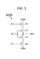
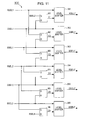
- FIG. 3 shows a circuit diagram of each of the clocked inverters 334 and 335.
- the control signal C1 is supplied to an N-channel transistor N2, and an inverted control signal C1' is supplied to a P-channel transistor P2.
- the inverted control signal C1' is a signal which is obtained by inverting the control signal C1 by the inverter 336. Accordingly, when the control signal C1 becomes active, the transistors P2 and N2 are turned on, so that the clocked inverters 334 and 335 operate, allowing the current to flow.
- the control signal C1 becomes active, the transistors P2 and N2 become turned on, so that transistors P1 and N1 operate to allow the breakthrough current to flow.
- the transistors P2 and N2 are turned off, so that the clocked inverters 334 and 335 do not operate, interrupting the breakthrough current to flow into the clocked inverters 334 and 335.
- the control signal C1 becomes active, TFTs 337 and 339 shown in FIG. 2 are turned on. For this reason, the potential of VSSH is supplied to the gate terminals of the TFTs 341 and 342.
- the common drain Cd has the potential of VDDH, so that the breakthrough current of all TFTs constituting the level shifter 321 does not flow.
- the clocked inverters 334 and 335 and the TFTs 337 and 339 have a function of controlling whether or not the level conversion operation performed based on the control signal C1.
- the R level shifter 321 does not consume power during a period that the level conversion operation is not performed.
- the clocked inverters 334 and 335 and the TFTs 337 and 339 contribute to a reduction in power consumption of the R level shifter 321 in cooperation with the control unit 310 described later.
- the signal level having a differential waveform at one end of each of the capacitors 331 and 332 converges to the voltage Vofs1 or Vofs2.
- a threshold voltage VthP is set to be lower than the voltage Vofs1. Accordingly, when the low-amplitude selection signal RSEL is not inverted for a long time in a circuit that does not have TFTs 338 and 340, the logical level of the low-amplitude selection signal RSEL may be not subjected to transition, whereas the high-amplitude selection signal RSEL' may be inverted.
- the TFTs 338 and 340 thus serve to prevent this erroneous operation.
- the gate potential of the TFT 341 exceeds the threshold value VthP due to the rising edge of the differential waveform, so that the TFT 341 is turned off, while the gate potential of the TFT 342 is larger than the threshold value VthN, so that the TFT 342 is turned on. For this reason, the potential of the common drain Cd becomes the low potential VSSH corresponding to the L level.
- the gate potential of the TFT 342 is maintained at the high potential VDDH, regardless of the offset voltage caused by the clocked inverter 335.
- the gate potential of the TFT 342 is not less than the threshold value VthN.
- the TFT 338 is turned off, so that the gate potential of the TFT 341 is one which has offset the voltage Vofs1 to the differential waveform of the low-amplitude selection signal RSEL.
- the gate potential of the TFT 341 is equal to or less than the threshold value VthP due to the falling edge of the differential waveform, so that the TFT 341 is turned on. Accordingly, the potential of the common drain Cd becomes the high potential VDDH corresponding to the H level.
- the gate potential of the TFT 341 is maintained at the low potential VSSH, regardless of the offset voltage caused by the clocked inverter 334.
- the gate potential of the TFT 341 does not exceed the threshold value VthP.
- the TFT 340 is turned off, so that the gate potential of the TFT 342 is one which has offset the voltage Vofs2 to the differential waveform of the low-amplitude selection signal RSEL. Accordingly, the R level shifter 321 operates stably with no erroneous operation, even when the same logical level covers the long time.
- the R memory Mr1 has a latch circuit composed of inverters 351 and 352, and TFTs 353 and 354.
- a set terminal S is connected to a gate of the TFT 353.
- the signal level of the set terminal is the H level
- the logical level of the control signal C1 is set to the H level.
- a gate of the TFT 354 is connected to a reset terminal R.
- the signal level of the reset terminal R is the H level
- the logical level of the control signal C1 is reset to the L level. That is, the R memory Mr1 serves as an SR flip-flop circuit.
- the low-amplitude selection signals become active cyclically in an order of RSEL, GSEL, BSEL, RSEL, GSEL, BSEL, ⁇ .
- the level shifter does not need to operate continuously, and it may operate only during a period in which the signal to be converted becomes active.
- control unit 310 generates the control signals which permit the operation of the level shifter, to which a corresponding low-amplitude selection signal is supplied, by using a preceding low-amplitude selection signal which precedes the corresponding low-amplitude selection signal and inhibit the operation of the level shifter by using a succeeding low-amplitude selection signal which follows the corresponding low-amplitude selection signal.
- FIG. 4 shows a timing chart of the low-amplitude selection signals and the control signals.
- the low-amplitude selection signal BSEL is supplied to the set terminal S of the R memory Mr1, while the low-amplitude selection signal GSEL is supplied to the reset terminal R of the R memory Mr1. Accordingly, when the low-amplitude selection signal BSEL becomes active at time t3, the control signal C1 becomes the H level, and then, when the low-amplitude selection signal GSEL becomes active at time t5, the control signal C1 becomes the L level. As a result, the control signal C1 becomes active during a period T1 ranging from the time t3 to the time t5, so that the R level shifter operates.
- the period Te during which the low-amplitude selection signal RSEL becomes active is included in the period T1, so that the R level shifter 321 may achieve a desired object.
- control signal C1 becomes inactive during a period in which the low-amplitude selection signal BSEL becomes active at time t6 after time t5, so that the R level shifter 231 does not operate.
- the R level shifter 231 does not operate during a period Tr ranging from time t2 to time t3.
- the breakthrough current is '0' during the period Tr, so that power consumption of the R shift register 321 may be reduced by two thirds as compared to a case in which the R level shifter operates continuously.
- the G level shifter 322 and the B level shifter 323 do not operate during periods Tg and Tb, respectively, so that power consumption may be reduced by two thirds, similarly to the R shift register 321.
- FIG. 5 is a block diagram showing an electrical configuration of essential parts of an electro-optical device according to a second embodiment of the present invention.
- This electro-optical device has the same configuration as that of the first embodiment except that the control unit 310 of the level shift circuit 300 is reset by a master reset signal MRST.
- the timing generating circuit 400 generates the master reset signal MRST which becomes active just after power is supplied.
- the master reset signal MRST preferably becomes active before the low-amplitude selection signals RSEL, GSEL, and BSEL become active.
- FIG. 6 shows a detailed configuration of the level shift circuit 300.
- the level shifters 321 to 323 have the same configuration as that of the first embodiment.
- the R memory Mr2, the G memory Mg2, and the B memory Mb2 differ from the memories Mr1, Mg1, and Mb1 of the first embodiment in that they have the master reset terminal MR.
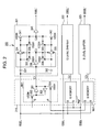
- FIG. 7 is a circuit diagram of the R memory Mr2
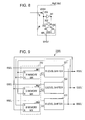
- FIG. 8 is a circuit diagram of the G memory Mg2 and the B memory Mb2.
- a TFT 356 is added parallel to the TFT 354.
- the TFT 356 is turned on when the potential on the master reset terminal MR becomes the H level, thereby making the control signal C1 inactive.
- an initial state of each memory Mr1, Mg1, and Mb1 is indefinite.
- the control signals C1 to C3 are not limited to be generated to permit the operations of the level shifters 321 to 323, respectively. For this reason, there is a case in which all of the control signals C1 to C3 become inactive when power is supplied. In this case, the level conversion is not performed even though the low-amplitude selection signals RSEL, GSEL, and BSEL become active.
- the levels of the set terminals S of the memories Mr1, Mg1, and Mb1 become sequentially the H level, so that the level shifters return to normal operations.
- the master reset signal MRST is supplied to the control unit 310. Then, the stored content in the R memory Mr2 is set to the operation permission state, and the stored contents in the G memory Mg2 and the B memory Mb2 are reset to the operation inhibition state.
- the low-amplitude selection signal which becomes active for the first time after power is supplied is RSEL. Accordingly, just after power is supplied, the level shifters 321 to 323 can be stable operated. As a result, the disturbance of the display image can be prevented from occurring.
- the Y transmission start pulse DY may be supplied as the master reset signal MRST. As described above, the Y transmission start pulse DY becomes active at the beginning of the vertical scanning period. In addition, the low-amplitude selection signals RSEL, GSEL, and BSEL become active after the active period of the Y transmission start pulse DY ends in each vertical scanning period. Accordingly, stable operation can be realized by using the Y transmission start pulse DY as the master reset signal MRST. In addition, the timing generating circuit 400 does not need to generate the master reset signal MRST separately from the Y transmission start pulse DY, so that the configuration of the timing generating circuit 400 may be simplified. In addition, the X transmission start pulse DX may be used as the master reset signal MRST.
- the X transmission start pulse DX is the signal which becomes active at the beginning of the horizontal scanning period, and the low-amplitude selection signals RSEL, GSEL, and BSEL become active after the X transmission start pulse DX become inactive in each horizontal scanning period. Accordingly, stable operation can be realized even when the X transmission start pulse DX is used as the master reset signal MRST, so that the configuration of the timing generating circuit 400 can be simplified.
- the control unit 310 generates the control signals C1 to C3 based on the low-amplitude selection signals RSEL, GSEL, and BSEL.
- the control unit 310 may generate the control signals C1 to C3 based on the high-amplitude selection signals RSEL', GSEL', and BSEL'.
- a level shift circuit 300A shown in FIG. 9 may be used instead of the level shift circuit 300.
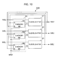
- a level shift circuit 300B shown in FIG. 10 may be used instead of the level shift circuit 300.
- the magnification may be 3 or more.
- the data line driving circuit 200 is provided outside the liquid crystal panel AA, it is necessary to provide input terminals at the end of the liquid crystal panel AA in order to supply the image signals x1, x2, ⁇ .
- the above-mentioned level shift circuit can reduce power consumption as the number of the selection signals increases.
- FIG. 11 is a block diagram showing a level shift circuit 300C corresponding to the demultiplxer having one input and six outputs.
- Memories M1 to M6 shown in FIG. 11 have the same configuration as that of the R memory Mr1 shown in FIG. 2, and level shifters 361 to 366 have the same configuration as that of the R level shifter 321 shown in FIG. 2.
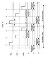
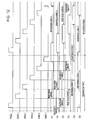
- FIG. 12 shows a timing chart of the level shift circuit 300C.
- the low-amplitude selection signals become active in an order of RSEL1, GSEL1, BSEL1, RSEL2, GSEL2, and BSEL2, and this cycle is repeated.
- the low-amplitude signal RSEL1 is supplied to the set terminal S of the memory M2 corresponding to the level shifter 332 and the low-amplitude selection signal BSEL1 is supplied to the reset terminal R thereof.
- the control signal C2 becomes active when the low-amplitude selection signal RSEL1 becomes the H level at time t1 and becomes inactive when the low-amplitude selection signal BSEL1 becomes the H level at time t3.
- control signal C2 maintains inactive until the low-amplitude selection signal RSEL1 becomes active again at time t2.
- the operation of the level shifter 332 is interrupted during a period in which the control signal C2 becomes inactive, so that the breakthrough current is '0'. Accordingly, power consumption of the level shifter 332 is reduced by one thirds as compared to a case in which the level shifter operates continuously.
- the low-amplitude selection signal for example, RSEL1 which becomes active just before a corresponding low-amplitude selection signal (for example, GSEL1) becomes active is used to store the operation permission state in the memory
- the low-amplitude selection signal for example, BSEL1 which becomes active just after the corresponding low-amplitude selection signal becomes active is used to store the operation inhibition state in the memory, so that the operation of the level shifter to which the corresponding low-amplitude selection signal is supplied according to the stored content in the memory is controlled.
- the low-amplitude selection signal which precedes or succeeds two low-amplitude selection signals may be used to rewrite the stored content in the memory.
- a preceding selection signal which precedes a corresponding low-amplitude selection signal is used to store the operation permission state in the memory
- a succeeding selection signal which succeeds the corresponding low-amplitude selection signal is used to store the operation inhibition state in the memory, so that the operation of the level shifter to which the corresponding low-amplitude selection signal is supplied may be controlled according to the stored content in the memory.
- the effect of reducing power consumption becomes maximized in the case of using the low-amplitude selection signal just before or just after the corresponding low-amplitude selection signal becomes active.
- the low-amplitude selection signal which precedes and succeeds two low-amplitude selection signals is used, the above-described effect of reducing power consumption is lowered because the stop period of the breakthrough current is shortened.
- the memories M1 to M6 may have the above-described master reset terminal, and in this case, the Y transmission start pulse DY or the X transmission start pulse DX may also be used as the master reset signal MRST. Furthermore, the high-amplitude selection signals may be supplied to the set terminals S and the reset terminals R of the memories M1 to M6, similarly to the above-described application.
- FIG. 13 shows a configuration of a mobile personal computer to which the electro-optical device according to each of the above-described embodiments is applied.
- the personal computer 2000 has an electro-optical device 1 as a display unit and a main body 2010.
- a power switch 2001 and a keyboard 2002 are installed in the main body 2010. This electro-optical device operates with reduced power consumption.
- FIG. 14 shows a configuration of a cellular phone to which the electro-optical device according to each of the above-described embodiments is applied.
- the cellular phone 3000 has a plurality of operating buttons 3001, scroll buttons 3002, and an electro-optical device as a display unit. By operating the scroll buttons 3002, a screen displayed on the electro-optical device is scrolled. According to the cellular phone 3000, power consumption of the electro-optical device is reduced, so that it may operate for a long time between charging operations.
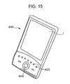
- FIG. 15 shows a configuration of a personal digital assistant (PDA) to which the electro-optical device according to each of the above-described embodiments is applied.
- the PDA 4000 has a plurality of operating buttons 4001, a power switch 4002, and an electro-optical device as a display unit.
- the power switch 4002 When the power switch 4002 is operated, a variety of information such as an address list or a schedule list is displayed on the electro-optical device.
- an electronic apparatus to which the electro-optical device according to the present invention is applied may include a digital still camera, a liquid crystal television, a viewfinder-type or monitor-direct-view-type video tape recorder, a car navigation device, a pager, an electronic organizer, an electronic calculator, a word processor, a workstation, a videophone, a POS (point of sale) terminal, an apparatus having a touch panel, and so on.
Landscapes
- Engineering & Computer Science (AREA)
- General Engineering & Computer Science (AREA)
- Mechanical Engineering (AREA)
- Chemical & Material Sciences (AREA)
- Crystallography & Structural Chemistry (AREA)
- Physics & Mathematics (AREA)
- Computer Hardware Design (AREA)
- General Physics & Mathematics (AREA)
- Theoretical Computer Science (AREA)
- Control Of Indicators Other Than Cathode Ray Tubes (AREA)
- Liquid Crystal Display Device Control (AREA)
- Logic Circuits (AREA)
- Liquid Crystal (AREA)
- Shift Register Type Memory (AREA)
Abstract
ÄObjectÜ To provide a level shift circuit which has reduced power consumption. <??>ÄSolving MeansÜ A level shift circuit 300 includes level shifters 321 to 323 and a control unit 310. The control unit 310 generates control signals C1 to C3 for controlling operation states of the level shifters 321 to 323, respectively. The control unit 321 has an R memory Mr1, a G memory Mgl, and a B memory Mb1. The G memory Mg1 has a stored content which is set to an operation permission state by means of a low-amplitude selection signal RSEL and which is reset to an operation inhibition state by means of a low-amplitude selection signal BSEL. Accordingly, during a period from the time when the low-amplitude selection signal BSEL becomes active up to the time when the low-amplitude selection signal RSEL becomes active, the operation of the level shifter 323 stops. As a result, power consumption decreases. <IMAGE>
Description
The present invention relates to a level shifter, a
level shift circuit, an electro-optical device, and to an
electronic apparatus which can reduce power consumption.
In recent years, electro-optical devices having an
electro-optical element such as a liquid crystal or an
organic light-emitting diode have been widely spread,
instead of a display device having a cathode ray tube. The
electro-optical devices are broadly classified as either a
passive matrix type or an active matrix type. The active
matrix type electro-optical device has scanning lines each
extending in a row direction, data lines each extending in a
column direction, and pixel electrodes provided
corresponding to intersections of the scanning lines and the
data lines. Furthermore, thin film transistors are provided
between the data lines and the pixel electrodes at the
intersections, which are turned on and off according to
scanning signals supplied to the scanning lines. In
addition, a counter electrode is provided corresponding to
the pixel electrodes, and an electro-optical material is
interposed between the pixel electrodes and the counter
electrode.
In order to drive the electro-optical material or the
thin film transistors, a relatively high voltage is needed.
On the other hand, an external control circuit which
supplies a clock signal, a control signal, and so on for
driving to the electro-optical device typically has CMOS
(Complementary Metal Oxide Semiconductor) circuits, and the
amplitude of a logical signal is in a range of from 3 to 5
V. Accordingly, the electro-optical device generally
converts a low-amplitude logical signal into a high-amplitude
logical signal by using an amplitude conversion
(hereinafter, simply referred to as a 'level shifter').
As the level shifter, a level shifter in which an input
signal is input via an alternating current (AC) coupling is
known (for example, see Patent Document 1).
[Patent Document 1] Japanese Unexamined Patent Application Publication No. 2003-110420 (Claim 1 and
Abstract)
[Patent Document 1] Japanese Unexamined Patent Application Publication No. 2003-110420 (
The level shifter converts the signal level, but it is
not necessary to operate continuously according to an action
of the signal to be converted. For example, in an electro-optical
device for color display, there is a case in which a
demultiplexer is used to output multiplexed data line
signals corresponding to respective colors of R, G, and B
from the data line driving circuit via one output terminal
and distribute the multiplexed data line signals to data
lines for R, G, and B. The demultiplexer outputs the data
line signals to the data lines of the respective colors
according to color selection signals of R, G, and B which
become exclusively active. In this case, it is common
practice to convert the signal levels of the color selection
signals by means of the level shifter. As such, the level
shifter is not needed to continuously operate, and it may
operate only during a period in which the input color
selection signal becomes active.
On the other hand, in a conventional level shifter,
when a power is supplied, some of the transistors are not
completely turned off, so that a small current flows between
a source and a drain of the transistor. For this reason,
there is a problem in that power is consumed during a period
in which it is not necessary to operate originally.
Accordingly, the present invention has been made in
consideration of the above-mentioned problems, and it is an
object of the present invention to provide a level shifter,
a level shift circuit, an electro-optical device, and an
electronic apparatus having reduced power consumption.
There is provided a level shift circuit according to
the present invention comprising a plurality of level
shifters being supplied with a plurality of selection
signals which become exclusively and sequentially active,
respectively, and converting signal levels of the selection
signals to output the converted signals; and a plurality of
control circuits, each supplying control signals, which
control an operation state of each of the level shifters, to
the corresponding level shifter. Each of the control
circuits generates the control signal indicating an
operation permission state by using an activated preceding
selection signal before the selection signal supplied to the
corresponding level shifter becomes active and the control
signal indicating an operation inhibition state by using an
activated succeeding selection signal after the selection
signal becomes active, and supplies the control signals to
the corresponding level shifter.
The plurality of selection signals become sequentially
active, so that the level shifter is not needed to
continuously operate and it may operate only during a period
in which the input selection signal becomes active.
According to the present invention, with a selection signal
as a reference, the control circuit permits the operation of
the level shifter by using a preceding selection signal to
the reference selection signal and inhibits the operation of
the level shifter by using a succeeding selection signal to
the reference selection signal. Accordingly, the level
shifter operates only during a necessary period and does not
operate during an unnecessary period. Thus, power
consumption can be reduced as compared to the case in which
the level shifter continuously operates.
In this case, the preceding selection signal preferably
becomes active just before the selection signal supplied to
the corresponding level shifter becomes active, and the
succeeding selection signal preferably becomes active just
after the selection signal supplied to the corresponding
level shifter becomes active. As a result, power
consumption can be most effectively reduced.
In addition, the control circuit may generate the
control signal by using the selection signal supplied to the
level shifter, or it may generate the control signal by
using the selection signal output from the level shifter.
It is necessary for the control circuit to specify the
period in which the corresponding level shifter operates,
and thus any selection signals before or after the level
conversion may be used to specify the timing.
In addition, in the above-described level shift
circuit, each of the control circuits preferably has a
memory circuit for storing the operation state, and the
memory circuit preferably stores the operation permission
state when the preceding selection signal becomes active and
the operation inhibition state when the succeeding selection
signal becomes active and outputs signals according to the
stored content as the control signals. In this case, the
operation state of the level shifter may be stored in the
memory, and thus the level shifter can be controlled.
In this case, the level shift circuit may further
comprise initializing means which executes an initialization
operation by setting the stored content of a predetermined
memory circuit to the operation permission state and by
resetting the stored content of other memory circuits to the
operation inhibition state, among the memory circuits. Just
after power is supplied to the level shift circuit, the
stored content of the memory circuit cannot be uniquely
determined, and thus the stored contents of all of the
memory circuits may indicate the operation inhibition state.
In this case, the operations of all of the level shifters
are inhibited, and thus the level conversion is not
performed even when the selection signal becomes active.
According to the present invention, the level shift circuit
has the initializing means, and thus the above-described
problem can be solved. Furthermore, the initializing means
sets only the stored content of the predetermined memory
circuit to an operation permission state and operate only
the level shifter corresponding to the predetermined memory
circuit and stop other level shifters. The selection
signals becomes sequentially active, so that the
predetermined memory circuit may be set to operate the level
shifter which is supplied with the selection signal active
for the first time after power is supplied. Accordingly,
power consumption can be reduced and an erroneous operation
can be prevented from being caused when power is supplied.
Next, there is provided a level shifter according to
the present invention which converts a signal level of an
input signal and outputs the converted signal as an output
signal. The level shifter comprises a first capacitive
element one end of which is supplied with the input signal;
a second capacitive element one end of which is connected to
the one end of the first capacitive element; a first
transistor whose gate is connected to the other end of the
first capacitive element and whose source is connected to a
high-potential supply line; a second transistor whose gate
is connected to the other end of the second capacitive
element, whose source is connected to a low-potential supply
line, and whose drain is connected to a drain of the first
transistor; a first clocked inverter to which power is
supplied from the high-potential supply line and the low-potential
supply line, the power supply being controlled
based on a control signal, and an input terminal and an
output terminal of which are connected to the gate of the
first transistor; a second clocked inverter to which power
is supplied from the high-potential supply line and the low-potential
supply line, the power supply being controlled
based on a control signal, and an input terminal and an
output terminal of which are connected to the gate of the
second transistor; and an inverter an input terminal of
which is connected to the drains of the first transistor and
the second transistor and which outputs the output signal
via an output terminal.
According to this level shifter, the first clocked
inverter serves as a means for supplying an offset voltage
(a bias voltage) to the gate of the first transistor, and
the second clocked inverter serves as a means for supplying
an offset voltage (a bias voltage) to the gate of the second
transistor. Further, as for the first and second clocked
inverters, the power supply is controlled based on the
control signal. Accordingly, the power supply can be
controlled by means of the control signal which is supplied
from an exterior. When the power supply is interrupted, the
first and second clocked inverters stop to operate, so that
the offset voltage is not supplied. Thus, the first and
second transistors stop to operate, and also the inverter
stops to operate. As a result, a breakthrough current does
not flow through the level shifter. According to the level
shifter, the operation state may be externally controlled,
so that it may operate during the necessary period, thereby
reducing power consumption. Moreover, in the above-described
level shift circuit, it is preferable to use the
level shifter.
Next, there is an electro-optical device according to
the present invention, the electro-optical device
comprising: the above-described level shift circuit; a
plurality of scanning lines; a plurality of data lines; a
plurality of electro-optical elements provided corresponding
to intersections of the scanning lines and the data lines; a
scanning line driving circuit for supplying scanning signals
to the plurality of scanning lines, respectively; a data
line driving circuit for generating a data signal which is
supplied to the plurality of data lines; and a plurality of
demultiplexing circuits provided for every predetermined
number of data lines. Each of the demultiplexing circuits
outputs the data signal to one data line selected among the
predetermined number of data lines based on a plurality of
selection signals output from the level shift circuit.
According to the present invention, the signal level of
the selection signal is converted by means of the level
shift circuit, and the converted selection signal is output
to the demultiplexer. The level shifter constituting the
level shift circuit can reduce the breakthrough current of
the level shifter during the period in which each of the
plurality of selection signals becomes inactive, so that
power consumption of the electro-optical device can be
reduced. In particular, when the data line driving circuit
is provided outside the electro-optical panel (for example,
a liquid crystal panel), at one end of the electro-optical
panel, it is necessary to form input terminals to which an
output signal of the data line driving circuit is input.
The number of the required input terminals increases as the
number of the data lines increases. On the other hand, in
order to prevent an electrical short between the input
terminals, it is preferable to reduce the number of the
input terminals. To this end, it is necessary to increase
the number of the selection signals by increasing the
magnification of the demultiplexer. According to the
present invention, the level shift circuit which can reduce
power consumption is adopted, and thus power consumption of
the electro-optical device can be drastically reduced when
the magnification of the demultiplexer increases.
Further, there is provided an electro-optical device
according to the present invention, the electro-optical
device comprising: the above-described level shift circuit
having the initializing means; a plurality of scanning
lines; a plurality of data lines; a plurality of electro-optical
elements provided corresponding to intersections of
the scanning lines and the data lines; a scanning line
driving circuit for supplying scanning signals to the
plurality of scanning lines, respectively; a data line
driving circuit for generating a data signal which is
supplied to the plurality of data lines; a plurality of
demultiplexing circuits provided for every predetermined
number of data lines; and timing generating means of
generating the plurality of selection signals which are
supplied to the level shift circuit. Each of the
demultiplexing circuits may output the data signal to one
data line selected among the predetermined number of data
lines based on the plurality of selection signals output
from the level shift circuit, the timing generating means
may generate an initialization signal and supplies it to the
initializing means prior to the generation of the plurality
of the selection signals after power is supplied, and the
initializing means may execute the initialization operation
based on the initialization signal.
According to the present invention, the timing
generating means generates the initialization signal prior
to the generation of the plurality of selection signals
after power is supplied, so that the selection signals can
be normally generated just after power is supplied. As a
result, disturbance on an image can be removed when power is
supplied.
Further, the timing generating means may generate a
first start signal which becomes active at a beginning of a
vertical scanning period and supply it to the scanning line
driving circuit, may generate a second start signal which
becomes active at a beginning of a horizontal scanning
period and supply it to the data line driving circuit, and
may supply the first start signal or the second start signal
to the initializing means, instead of generating the
initialization signal and supplying it to the initializing
means. In addition, the initializing means may execute the
initialization operation based on the first start signal or
the second start signal supplied from the timing generating
means. According to the present invention, the timing
generating means is needed to generate the initialization
signal, and thus the configuration can be simplified.
Next, an electronic apparatus according to the present
invention has the above-described electro-optical device.
In this case, power consumption of the electronic apparatus
can be reduced. Such an electronic apparatus may include,
for example, a personal computer, a cellular phone, a PDA
(personal digital assistant), and so on.
FIG. 1 is a block diagram showing an electrical
configuration of an electro-optical device according to a
first embodiment of the present invention. The electro-optical
device uses a liquid crystal as an electro-optical
material, and has a liquid crystal panel AA, a timing
generating circuit 400, and an image processing circuit 500.
In the liquid crystal panel AA, an element substrate on
which thin film transistors (hereinafter, referred to as
'TFTs') are formed and a counter substrate are bonded by a
constant interval so that electrode forming surfaces of the
respective substrates face each other, and a liquid crystal
is interposed therebetween. On the element substrate of the
liquid crystal panel AA, an image display region A, a
scanning line driving circuit 100, a data line driving
circuit 200, a level shift circuit 300, and demultiplexers
DMP1 to DMPn are formed.
Input image data Din supplied to the electro-optical
device has, for example, a three-bit parallel format. The
timing generating circuit 400 generates a Y clock signal
YCK, an inverted Y clock signal YCKB, and a Y transmission
start pulse DY in synchronization with input image data Din
and supplies them to the scanning line driving circuit 100.
In addition, the timing generating circuit 400 generates an
X clock signal XCK, an inverted X clock signal XCKB, and an
X transmission start pulse DX in synchronization with input
image data Din and supplies them to the data line driving
circuit 200. The Y transmission start pulse DY is a pulse
of a vertical scanning period and becomes active only during
a predetermined period from the beginning of the vertical
scanning period. On the other hand, the X transmission
start pulse DX is a pulse of a horizontal scanning period
and becomes active only during a predetermined period from
the beginning of the horizontal scanning period.
The scanning line driving circuit 100 has shift
registers and sequentially transmits the Y transmission
start pulse DY in synchronization with the Y clock signal
YCK and the inverted Y clock signal YCKB and sequentially
generates scanning signals Y1, Y2, ···, and Ym.
The image processing circuit 500 performs gamma
correction or the like on input image data Din to improve
light transmission characteristics of the liquid crystal
panel AA, generates output image data Dout, and supplies it
to the data line driving circuit 200. The data line driving
circuit 200 has shift registers, latch circuits, and DA
(Digital-to-Analog) conversion circuits. The shift
registers sequentially transmit the X transmission start
pulse DX in synchronization with the X clock signal XCK and
the inverted Y clock signal YCKB and generates latch pulses.
The latch circuits latch output image data Dout by using the
latch pulses. The DA conversion circuits convert the output
signals of the latch circuits by using the DA conversion to
generate image signals x1, x2, ···, xn, respectively. The
signals for R, B, and G are multiplexed on each of the image
signals x1, x2, ···, xn in a time-division manner.
Each of the demultiplexers DMP1 to DMPn has three
switches SW1, SW2, and SW3, each being composed of the TFT.
High-amplitude selection signals RSEL', GSEL', and BSEL' are
supplied to the switch SW1, SW2, and SW3, respectively.
The level shift circuit 300 converts the signal levels
of low-amplitude selection signals RSEL, GSEL, and BSEL from
a low amplitude to a high amplitude to generate the high-amplitude
selection signals RSEL', GSEL', and BSEL',
respectively. L and H levels of the low-amplitude selection
signals RSEL, GSEL, and BSEL are VSSL and VDDL,
respectively, and L and H levels of the high-amplitude
selection signals RSEL', GSEL', and BSEL' are VSSH and VDDH,
respectively. The details of the level shift circuit 300
will be described later.
Next, in the image display region A, m scanning lines 2
(where m is a natural number of 2 or more) are arranged
parallel to an X direction and 3n data lines 3 (where n is a
natural number of 2 or more) are arranged parallel to a Y
direction. In a vicinity of each intersection of the
scanning lines 2 and the data lines 3, a gate of a TFT 50 is
connected to the scanning line 2, a source of the TFT 50 is
connected to the data line 3, and a drain of the TFT 50 is
connected to a pixel electrode 6. Then, each pixel is
composed of the pixel electrode 6, a counter electrode
formed on a counter substrate, and a liquid crystal
interposed between these two electrodes. As a result, the
pixels are arranged in a matrix shape to correspond to the
intersections of the scanning lines 2 and the data lines 3.
In addition, pulsed scanning signals Y1, Y2, ..., and
Ym are line-sequentially applied to the scanning lines 2 to
each of which the gate of the TFT 50 is connected. For this
reason, if the scanning signal is supplied to the scanning
line 2, the TFT 50 connected to the corresponding scanning
line 2 is turned on, so that data line signals X1, X2, ···,
and X3n supplied from the data lines 3 at the predetermined
timing are sequentially written onto the corresponding
pixels and stored for a predetermined period.
The orientation and order of liquid crystal molecules
change according to a potential level applied to each pixel,
so that a gray-scale display resulting from the optical
modulation can be realized. For example, while the amount
of light passing through the liquid crystal is limited as
the applied potential increases in a normally white mode, it
is mitigated as the applied potential increases in a
normally-black mode. And thus, light having a contrast
according to the image signal is emitted for each pixel in
the entire liquid crystal display device. For this reason,
a predetermined display can be realized.
Next, the details of the level shift circuit 300 will
be described. The level shift circuit 300 has an R level
shifter 321, a G level shifter 322, a B level shifter 323,
and a control unit 310 for controlling the operations of the
level shifters 321 to 323, as shown in FIG. 1. The control
unit 310 generates control signals C1, C2, and C3 for
controlling the operations of the level shifters 321 to 323,
respectively.
FIG. 2 shows a detailed configuration of the level
shift circuit 300. The G level shifter 322 and the B level
shifter 323 have the same configuration as that of the R
level shifter 321. In addition, the control unit 310 has an
R memory Mr1, a G memory Mg1, and a B memory Mb1 that
correspond to the level shifters 321 to 323, respectively.
Each of the G memory Mg and the B memory Mb1 has the same
configuration as that of the R memory Mr1 and has a set
terminal S and a reset terminal R. These memories serve as
control circuits which control the corresponding level
shifters.
The low-amplitude selection signal RSEL is supplied to
one end of each of capacitors (capacitance) 331 and 332 in
the R level shifter 321. On the other hand, the other end
of the capacitor 331 is connected to a gate of a P-channel
TFT 341, and the other end of the capacitor 332 is connected
to a gate of an N-channel TFT 342.
Next, a source of the TFT 341 is connected to a power
supply line of the high potential VDDH, a source of the TFT
342 is connected to a power supply line of the low potential
VSSH, and drains of the TFTs 341 and 342 are connected to
each other in common. In this case, the common drain of the
TFTs 341 and 342 is represented by reference numeral Cd.
The common drain Cd of the TFTs 341 and 342 is connected to
an input terminal of the inverter 343. From an output
terminal of the inverter 343, the high-amplitude selection
signal RSEL' is output.
A voltage Vofs1 is offset by a clocked inverter 334
constituting a first offset circuit to the other end of the
capacitor 331, that is, the gate of the TFT 341. Similarly,
a voltage Vofs2 is offset by a clocked inverter 335
constituting a second offset circuit to the other end of the
capacitor 332 (a gate Nin). The voltages Vofs1 and Vofs2
are potentials which change according to the output state of
the level shifter.
FIG. 3 shows a circuit diagram of each of the clocked
inverters 334 and 335. The control signal C1 is supplied to
an N-channel transistor N2, and an inverted control signal
C1' is supplied to a P-channel transistor P2. The inverted
control signal C1' is a signal which is obtained by
inverting the control signal C1 by the inverter 336.
Accordingly, when the control signal C1 becomes active, the
transistors P2 and N2 are turned on, so that the clocked
inverters 334 and 335 operate, allowing the current to flow.
Here, when the control signal C1 becomes active, the
transistors P2 and N2 become turned on, so that transistors
P1 and N1 operate to allow the breakthrough current to flow.
Alternatively, when the control signal C1 becomes inactive,
the transistors P2 and N2 are turned off, so that the
clocked inverters 334 and 335 do not operate, interrupting
the breakthrough current to flow into the clocked inverters
334 and 335. Furthermore, when the control signal C1
becomes active, TFTs 337 and 339 shown in FIG. 2 are turned
on. For this reason, the potential of VSSH is supplied to
the gate terminals of the TFTs 341 and 342. As a result,
the common drain Cd has the potential of VDDH, so that the
breakthrough current of all TFTs constituting the level
shifter 321 does not flow.
As such, the clocked inverters 334 and 335 and the TFTs
337 and 339 have a function of controlling whether or not
the level conversion operation performed based on the
control signal C1. The R level shifter 321 does not consume
power during a period that the level conversion operation is
not performed. The clocked inverters 334 and 335 and the
TFTs 337 and 339 contribute to a reduction in power
consumption of the R level shifter 321 in cooperation with
the control unit 310 described later.
When the low-amplitude selection signal RSEL is not
inverted for a long time, the signal level having a
differential waveform at one end of each of the capacitors
331 and 332 converges to the voltage Vofs1 or Vofs2. As
described above, a threshold voltage VthP is set to be lower
than the voltage Vofs1. Accordingly, when the low-amplitude
selection signal RSEL is not inverted for a long time in a
circuit that does not have TFTs 338 and 340, the logical
level of the low-amplitude selection signal RSEL may be not
subjected to transition, whereas the high-amplitude
selection signal RSEL' may be inverted. The TFTs 338 and
340 thus serve to prevent this erroneous operation.
When the low-amplitude selection signal RSEL is
subjected to the transition from the low potential VSSL to
the high potential VDDL, the gate potential of the TFT 341
exceeds the threshold value VthP due to the rising edge of
the differential waveform, so that the TFT 341 is turned
off, while the gate potential of the TFT 342 is larger than
the threshold value VthN, so that the TFT 342 is turned on.
For this reason, the potential of the common drain Cd
becomes the low potential VSSH corresponding to the L level.
Thus, when the TFT 340 is turned on, the gate potential of
the TFT 342 is maintained at the high potential VDDH,
regardless of the offset voltage caused by the clocked
inverter 335. Then, even when the low-amplitude selection
signal RSEL becomes the high potential VDDL covering the
long time, the gate potential of the TFT 342 is not less
than the threshold value VthN. On the other hand, the TFT
338 is turned off, so that the gate potential of the TFT 341
is one which has offset the voltage Vofs1 to the
differential waveform of the low-amplitude selection signal
RSEL.
In addition, when the low-amplitude selection signal
RSEL is subjected to the transition from the high potential
VDDL to the low potential VSSL, the gate potential of the
TFT 341 is equal to or less than the threshold value VthP
due to the falling edge of the differential waveform, so
that the TFT 341 is turned on. Accordingly, the potential
of the common drain Cd becomes the high potential VDDH
corresponding to the H level. Thus, when the TFT 338 is
turned on, the gate potential of the TFT 341 is maintained
at the low potential VSSH, regardless of the offset voltage
caused by the clocked inverter 334. Then, even when the
low-amplitude selection signal RSEL becomes the low
potential VSSL covering the long time, the gate potential of
the TFT 341 does not exceed the threshold value VthP. On
the other hand, the TFT 340 is turned off, so that the gate
potential of the TFT 342 is one which has offset the voltage
Vofs2 to the differential waveform of the low-amplitude
selection signal RSEL. Accordingly, the R level shifter 321
operates stably with no erroneous operation, even when the
same logical level covers the long time.
Next, the R memory Mr1 as a part of the control unit
310 will be described. Moreover, the G memory Mg1 and the B
memory Mb1 have the same configuration as that of the R
memory Mr1. The R memory Mr1 has a latch circuit composed
of inverters 351 and 352, and TFTs 353 and 354. A set
terminal S is connected to a gate of the TFT 353. When the
signal level of the set terminal is the H level, the logical
level of the control signal C1 is set to the H level. A
gate of the TFT 354 is connected to a reset terminal R.
When the signal level of the reset terminal R is the H
level, the logical level of the control signal C1 is reset
to the L level. That is, the R memory Mr1 serves as an SR
flip-flop circuit.
As described above, the low-amplitude selection signals
become active cyclically in an order of RSEL, GSEL, BSEL,
RSEL, GSEL, BSEL, ···. As such, when converting the signal
level of each signal of a signal group having the cyclically
activated signals in such a manner, the level shifter does
not need to operate continuously, and it may operate only
during a period in which the signal to be converted becomes
active. Accordingly, the control unit 310 generates the
control signals which permit the operation of the level
shifter, to which a corresponding low-amplitude selection
signal is supplied, by using a preceding low-amplitude
selection signal which precedes the corresponding low-amplitude
selection signal and inhibit the operation of the
level shifter by using a succeeding low-amplitude selection
signal which follows the corresponding low-amplitude
selection signal.
FIG. 4 shows a timing chart of the low-amplitude
selection signals and the control signals. The low-amplitude
selection signal BSEL is supplied to the set
terminal S of the R memory Mr1, while the low-amplitude
selection signal GSEL is supplied to the reset terminal R of
the R memory Mr1. Accordingly, when the low-amplitude
selection signal BSEL becomes active at time t3, the control
signal C1 becomes the H level, and then, when the low-amplitude
selection signal GSEL becomes active at time t5,
the control signal C1 becomes the L level. As a result, the
control signal C1 becomes active during a period T1 ranging
from the time t3 to the time t5, so that the R level shifter
operates. The period Te during which the low-amplitude
selection signal RSEL becomes active is included in the
period T1, so that the R level shifter 321 may achieve a
desired object.
On the other hand, the control signal C1 becomes
inactive during a period in which the low-amplitude
selection signal BSEL becomes active at time t6 after time
t5, so that the R level shifter 231 does not operate. In
addition, the R level shifter 231 does not operate during a
period Tr ranging from time t2 to time t3. The breakthrough
current is '0' during the period Tr, so that power
consumption of the R shift register 321 may be reduced by
two thirds as compared to a case in which the R level
shifter operates continuously. In addition, the G level
shifter 322 and the B level shifter 323 do not operate
during periods Tg and Tb, respectively, so that power
consumption may be reduced by two thirds, similarly to the R
shift register 321.
FIG. 5 is a block diagram showing an electrical
configuration of essential parts of an electro-optical
device according to a second embodiment of the present
invention. This electro-optical device has the same
configuration as that of the first embodiment except that
the control unit 310 of the level shift circuit 300 is reset
by a master reset signal MRST. The timing generating
circuit 400 generates the master reset signal MRST which
becomes active just after power is supplied. In addition,
the master reset signal MRST preferably becomes active
before the low-amplitude selection signals RSEL, GSEL, and
BSEL become active.
FIG. 6 shows a detailed configuration of the level
shift circuit 300. The level shifters 321 to 323 have the
same configuration as that of the first embodiment. On the
other hand, the R memory Mr2, the G memory Mg2, and the B
memory Mb2 differ from the memories Mr1, Mg1, and Mb1 of the
first embodiment in that they have the master reset terminal
MR. FIG. 7 is a circuit diagram of the R memory Mr2, and
FIG. 8 is a circuit diagram of the G memory Mg2 and the B
memory Mb2. First, in the R memory Mr2, a TFT 355 is added
parallel to the TFT 353. The TFT 355 is turned on when the
potential on the master reset terminal MR becomes the H
level, thereby making the control signal C1 active. On the
other hand, in each of the G memory Mg2 and the B memory
Mb2, a TFT 356 is added parallel to the TFT 354. The TFT
356 is turned on when the potential on the master reset
terminal MR becomes the H level, thereby making the control
signal C1 inactive.
In the above-described control unit 310 of the first
embodiment, an initial state of each memory Mr1, Mg1, and
Mb1 is indefinite. Specifically, the control signals C1 to
C3 are not limited to be generated to permit the operations
of the level shifters 321 to 323, respectively. For this
reason, there is a case in which all of the control signals
C1 to C3 become inactive when power is supplied. In this
case, the level conversion is not performed even though the
low-amplitude selection signals RSEL, GSEL, and BSEL become
active. When one horizontal scanning period passed,
however, the levels of the set terminals S of the memories
Mr1, Mg1, and Mb1 become sequentially the H level, so that
the level shifters return to normal operations.
According to the present embodiment, the master reset
signal MRST is supplied to the control unit 310. Then, the
stored content in the R memory Mr2 is set to the operation
permission state, and the stored contents in the G memory
Mg2 and the B memory Mb2 are reset to the operation
inhibition state. In this embodiment, the low-amplitude
selection signal which becomes active for the first time
after power is supplied is RSEL. Accordingly, just after
power is supplied, the level shifters 321 to 323 can be
stable operated. As a result, the disturbance of the
display image can be prevented from occurring.
Moreover, the Y transmission start pulse DY may be
supplied as the master reset signal MRST. As described
above, the Y transmission start pulse DY becomes active at
the beginning of the vertical scanning period. In addition,
the low-amplitude selection signals RSEL, GSEL, and BSEL
become active after the active period of the Y transmission
start pulse DY ends in each vertical scanning period.
Accordingly, stable operation can be realized by using the Y
transmission start pulse DY as the master reset signal MRST.
In addition, the timing generating circuit 400 does not need
to generate the master reset signal MRST separately from the
Y transmission start pulse DY, so that the configuration of
the timing generating circuit 400 may be simplified. In
addition, the X transmission start pulse DX may be used as
the master reset signal MRST. The X transmission start
pulse DX is the signal which becomes active at the beginning
of the horizontal scanning period, and the low-amplitude
selection signals RSEL, GSEL, and BSEL become active after
the X transmission start pulse DX become inactive in each
horizontal scanning period. Accordingly, stable operation
can be realized even when the X transmission start pulse DX
is used as the master reset signal MRST, so that the
configuration of the timing generating circuit 400 can be
simplified.
(1) In the above-described first and second
embodiments, the control unit 310 generates the control
signals C1 to C3 based on the low-amplitude selection
signals RSEL, GSEL, and BSEL. However, the control unit 310
may generate the control signals C1 to C3 based on the high-amplitude
selection signals RSEL', GSEL', and BSEL'. For
example, in the electro-optical device of the first
embodiment as shown in FIG. 1, a level shift circuit 300A
shown in FIG. 9 may be used instead of the level shift
circuit 300. In addition, in the electro-optical device of
the second embodiment as shown in FIG. 5, a level shift
circuit 300B shown in FIG. 10 may be used instead of the
level shift circuit 300.
(2) In the above-described first and second embodiments
and the application, a configuration of one input and three
outputs is used for the demultiplexers DMP1 to DMPn,
however, the magnification may be 3 or more. When the data
line driving circuit 200 is provided outside the liquid
crystal panel AA, it is necessary to provide input terminals
at the end of the liquid crystal panel AA in order to supply
the image signals x1, x2, ···. In such a configuration, it
is important to reduce the number of the input terminals in
order to prevent the electrical short between the input
terminals. In this case, it is effective to increase the
magnification of the demultiplexer. However, when the
magnification of the demultiplexer increases, the number of
the selection signals increases, which results in increasing
the number of the level shifters, so that power consumption
increases. The above-mentioned level shift circuit can
reduce power consumption as the number of the selection
signals increases.
For example, it is assumed that a demultiplxer having
one input and six outputs is used. FIG. 11 is a block
diagram showing a level shift circuit 300C corresponding to
the demultiplxer having one input and six outputs. Memories
M1 to M6 shown in FIG. 11 have the same configuration as
that of the R memory Mr1 shown in FIG. 2, and level shifters
361 to 366 have the same configuration as that of the R
level shifter 321 shown in FIG. 2.
FIG. 12 shows a timing chart of the level shift circuit
300C. As shown in FIG. 12, the low-amplitude selection
signals become active in an order of RSEL1, GSEL1, BSEL1,
RSEL2, GSEL2, and BSEL2, and this cycle is repeated. In
this case, in the level shifter 332, the low-amplitude
signal RSEL1 is supplied to the set terminal S of the memory
M2 corresponding to the level shifter 332 and the low-amplitude
selection signal BSEL1 is supplied to the reset
terminal R thereof. Accordingly, the control signal C2
becomes active when the low-amplitude selection signal RSEL1
becomes the H level at time t1 and becomes inactive when the
low-amplitude selection signal BSEL1 becomes the H level at
time t3. Then, the control signal C2 maintains inactive
until the low-amplitude selection signal RSEL1 becomes
active again at time t2. The operation of the level shifter
332 is interrupted during a period in which the control
signal C2 becomes inactive, so that the breakthrough current
is '0'. Accordingly, power consumption of the level shifter
332 is reduced by one thirds as compared to a case in which
the level shifter operates continuously.
In this example, the low-amplitude selection signal
(for example, RSEL1) which becomes active just before a
corresponding low-amplitude selection signal (for example,
GSEL1) becomes active is used to store the operation
permission state in the memory, and the low-amplitude
selection signal (for example, BSEL1) which becomes active
just after the corresponding low-amplitude selection signal
becomes active is used to store the operation inhibition
state in the memory, so that the operation of the level
shifter to which the corresponding low-amplitude selection
signal is supplied according to the stored content in the
memory is controlled. Alternatively, instead of the low-amplitude
selection signal just before or just after the
corresponding low-amplitude selection signal becomes active,
the low-amplitude selection signal which precedes or
succeeds two low-amplitude selection signals may be used to
rewrite the stored content in the memory. In summary, a
preceding selection signal which precedes a corresponding
low-amplitude selection signal is used to store the
operation permission state in the memory, and a succeeding
selection signal which succeeds the corresponding low-amplitude
selection signal is used to store the operation
inhibition state in the memory, so that the operation of the
level shifter to which the corresponding low-amplitude
selection signal is supplied may be controlled according to
the stored content in the memory. Above all things, the
effect of reducing power consumption becomes maximized in
the case of using the low-amplitude selection signal just
before or just after the corresponding low-amplitude
selection signal becomes active. When the low-amplitude
selection signal which precedes and succeeds two low-amplitude
selection signals is used, the above-described
effect of reducing power consumption is lowered because the
stop period of the breakthrough current is shortened.
In this application, the memories M1 to M6 may have the
above-described master reset terminal, and in this case, the
Y transmission start pulse DY or the X transmission start
pulse DX may also be used as the master reset signal MRST.
Furthermore, the high-amplitude selection signals may be
supplied to the set terminals S and the reset terminals R of
the memories M1 to M6, similarly to the above-described
application.
Next, an electronic apparatus to which the electro-optical
device according to the present invention is applied
will be described. FIG. 13 shows a configuration of a
mobile personal computer to which the electro-optical device
according to each of the above-described embodiments is
applied. The personal computer 2000 has an electro-optical
device 1 as a display unit and a main body 2010. A power
switch 2001 and a keyboard 2002 are installed in the main
body 2010. This electro-optical device operates with
reduced power consumption.
FIG. 14 shows a configuration of a cellular phone to
which the electro-optical device according to each of the
above-described embodiments is applied. The cellular phone
3000 has a plurality of operating buttons 3001, scroll
buttons 3002, and an electro-optical device as a display
unit. By operating the scroll buttons 3002, a screen
displayed on the electro-optical device is scrolled.
According to the cellular phone 3000, power consumption of
the electro-optical device is reduced, so that it may
operate for a long time between charging operations.
FIG. 15 shows a configuration of a personal digital
assistant (PDA) to which the electro-optical device
according to each of the above-described embodiments is
applied. The PDA 4000 has a plurality of operating buttons
4001, a power switch 4002, and an electro-optical device as
a display unit. When the power switch 4002 is operated, a
variety of information such as an address list or a schedule
list is displayed on the electro-optical device.
Furthermore, instead of the electronic apparatuses
shown in FIGS. 13 to 15, an electronic apparatus to which
the electro-optical device according to the present
invention is applied may include a digital still camera, a
liquid crystal television, a viewfinder-type or monitor-direct-view-type
video tape recorder, a car navigation
device, a pager, an electronic organizer, an electronic
calculator, a word processor, a workstation, a videophone, a
POS (point of sale) terminal, an apparatus having a touch
panel, and so on.
Claims (11)
- A level shift circuit comprising:wherein each of the control circuits generates the control signal indicating an operation permission state by using an activated preceding selection signal before the selection signal supplied to the corresponding level shifter becomes active and the control signal indicating an operation inhibition state by using an activated succeeding selection signal after the selection signal becomes active, and supplies the control signals to the corresponding level shifter.a plurality of level shifters being supplied with a plurality of selection signals which become exclusively and sequentially active, respectively, and converting signal levels of the selection signals to output the converted signals; anda plurality of control circuits, each supplying control signals, which control an operation state of each of the level shifters, to the corresponding level shifter,
- The level shift circuit according to Claim 1,
wherein the preceding selection signal becomes active just before the selection signal supplied to the corresponding level shifter becomes active, and the succeeding selection signal becomes active just after the selection signal supplied to the corresponding level shifter becomes active. - The level shift circuit according to Claim 1 or 2,
wherein each of the control circuits generates the control signals using the selection signal supplied to the level shifter. - The level shift circuit according to Claim 1 or 2,
wherein the control circuit generates the control signals using the selection signal output from the level shifter. - The level shift circuit according to any one of Claims 1 to 4,
wherein each of the control circuits has a memory circuit for storing the operation state, and the memory circuit stores the operation permission state when the preceding selection signal becomes active and the operation inhibition state when the succeeding selection signal becomes active and outputs signals according to the stored content as the control signals. - The level shift circuit according to Claim 5, further comprising:initializing means which executes an initialization operation by setting the stored content of a predetermined memory circuit to the operation permission state and by resetting the stored content of other memory circuits to the operation inhibition state, among the memory circuits.
- A level shifter which converts a signal level of an input signal and outputs the converted signal as an output signal, the level shifter comprising:a first capacitive element one end of which is supplied with the input signal;a second capacitive element one end of which is connected to the one end of the first capacitive element;a first transistor whose gate is connected to the other end of the first capacitive element and whose source is connected to a high-potential supply line;a second transistor whose gate is connected to the other end of the second capacitive element, whose source is connected to a low-potential supply line, andwhose drain is connected to a drain of the first transistor;a first clocked inverter to which power is supplied from the high-potential supply line and the low-potential supply line, the power supply being controlled based on a control signal, and an input terminal and an output terminal of which are connected to the gate of the first transistor;a second clocked inverter to which power is supplied from the high-potential supply line and the low-potential supply line, the power supply being controlled based on a control signal, and an input terminal and an output terminal of which are connected to the gate of the second transistor; andan inverter of which input terminal is connected to the drains of the first transistor and the second transistor and which outputs the output signal via an output terminal.
- An electro-optical device comprising:wherein each of the demultiplexing circuits outputs the data signal to one data line selected among the predetermined number of data lines based on a plurality of selection signals output from the level shift circuit.a level shift circuit as claimed in any one of Claims 1 to 5;a plurality of scanning lines;a plurality of data lines;a plurality of electro-optical elements provided corresponding to intersections of the scanning lines and the data lines;a scanning line driving circuit for supplying scanning signals to the plurality of scanning lines, respectively;a data line driving circuit for generating a data signal which is supplied to the plurality of data lines; anda plurality of demultiplexing circuits provided for every predetermined number of data lines,
- An electro-optical device comprising:wherein each of the demultiplexing circuits outputs the data signal to one data line selected among the predetermined number of data lines based on the plurality of selection signals output from the level shift circuit,a level shift circuit as claimed in Claim 6;a plurality of scanning lines;a plurality of data lines;a plurality of electro-optical elements provided corresponding to intersections of the scanning lines and the data lines;a scanning line driving circuit for supplying scanning signals to the plurality of scanning lines, respectively;a data line driving circuit for generating a data signal which is supplied to the plurality of data lines;a plurality of demultiplexing circuits provided for every predetermined number of data lines; andtiming generating means of generating the plurality of selection signals which are supplied to the level shift circuit,
the timing generating means generates an initialization signal and supplies it to the initializing means prior to the generation of the plurality of the selection signals after power is supplied, and
the initializing means executes the initialization operation based on the initialization signal. - The electro-optical device according to Claim 9,
wherein the timing generating means generates a first start signal which becomes active at a beginning of a vertical scanning period and supplies it to the scanning line driving circuit, generates a second start signal which becomes active at a beginning of a horizontal scanning period and supplies it to the data line driving circuit, and supplies the first start signal or the second start signal to the initializing means, instead of generating the initialization signal and supplying it to the initializing means, and
the initializing means executes the initialization operation based on the first start signal or the second start signal supplied from the timing generating means. - An electronic apparatus comprising an electro-optical device as claimed in any one of Claims 8 to 10.
Applications Claiming Priority (2)
| Application Number | Priority Date | Filing Date | Title |
|---|---|---|---|
| JP2004109223A JP4127232B2 (en) | 2004-04-01 | 2004-04-01 | Level shifter, level shift circuit, electro-optical device, and electronic apparatus |
| JP2004109223 | 2004-04-01 |
Publications (1)
| Publication Number | Publication Date |
|---|---|
| EP1585103A2 true EP1585103A2 (en) | 2005-10-12 |
Family
ID=34909461
Family Applications (1)
| Application Number | Title | Priority Date | Filing Date |
|---|---|---|---|
| EP05006871A Withdrawn EP1585103A2 (en) | 2004-04-01 | 2005-03-30 | Level shifter, level shift circuit, electro-optical device, and electronic apparatus |
Country Status (6)
| Country | Link |
|---|---|
| US (1) | US7136311B2 (en) |
| EP (1) | EP1585103A2 (en) |
| JP (1) | JP4127232B2 (en) |
| KR (1) | KR100714817B1 (en) |
| CN (1) | CN100525106C (en) |
| TW (1) | TW200604981A (en) |
Families Citing this family (15)
| Publication number | Priority date | Publication date | Assignee | Title |
|---|---|---|---|---|
| TWI344625B (en) | 2005-03-08 | 2011-07-01 | Epson Imaging Devices Corp | Driving circuit of display device, driving circuit of electro-optical device, and electronic apparatus |
| US7830176B2 (en) * | 2006-07-27 | 2010-11-09 | Arm Limited | Controlling signal levels on a signal line within an integrated circuit |
| US20080117190A1 (en) * | 2006-11-22 | 2008-05-22 | Chien-Ru Chen | Method and driver for driving a display |
| KR20090050730A (en) * | 2007-11-16 | 2009-05-20 | 삼성전자주식회사 | Display device and control method |
| JP4674280B2 (en) * | 2008-03-13 | 2011-04-20 | 奇美電子股▲ふん▼有限公司 | Demultiplexer, electronic device using the same, and liquid crystal display device |
| US9270273B2 (en) | 2011-10-28 | 2016-02-23 | Texas Instruments Incorporated | Level shifter |
| US8988960B2 (en) * | 2012-11-29 | 2015-03-24 | Nvidia Corporation | Technique for improving static random-access memory sense amplifier voltage differential |
| JP2014179723A (en) * | 2013-03-14 | 2014-09-25 | Seiko Epson Corp | Level shift circuit, electro-optical device and electronic apparatus |
| CN104253607B (en) * | 2013-06-25 | 2018-01-23 | 英业达科技有限公司 | Level adjusting circuit |
| US9607539B2 (en) * | 2014-12-31 | 2017-03-28 | Shenzhen China Star Optoelectronics Technology Co., Ltd. | Display panel capable of reducing a voltage level changing frequency of a select signal and drive circuit thereof |
| DE102016109114B4 (en) * | 2016-05-18 | 2025-06-18 | Infineon Technologies Ag | Level converter circuit, as well as measuring arrangement and chip with such a level converter circuit |
| DE102016109118A1 (en) | 2016-05-18 | 2017-11-23 | Infineon Technologies Ag | Circuit architecture for a measuring device, a level converter circuit, a charge pumping stage and a charge pump and method for operating these |
| JP6757352B2 (en) * | 2018-03-28 | 2020-09-16 | シャープ株式会社 | Active matrix board and display device |
| CN115188306B (en) * | 2021-04-02 | 2025-07-22 | 格科微电子(上海)有限公司 | Pixel refreshing method and device, storage medium and display |
| CN116564222B (en) * | 2023-07-07 | 2023-11-24 | 惠科股份有限公司 | Display device driving method and display device |
Family Cites Families (15)
| Publication number | Priority date | Publication date | Assignee | Title |
|---|---|---|---|---|
| TW423162B (en) * | 1997-02-27 | 2001-02-21 | Toshiba Corp | Power voltage supplying circuit and semiconductor memory including the same |
| JPH11220380A (en) | 1998-02-03 | 1999-08-10 | Sony Corp | Level shift circuit |
| JP3858486B2 (en) * | 1998-11-26 | 2006-12-13 | セイコーエプソン株式会社 | Shift register circuit, electro-optical device and electronic apparatus |
| JP3473745B2 (en) * | 1999-05-28 | 2003-12-08 | シャープ株式会社 | Shift register and image display device using the same |
| JP3426541B2 (en) * | 1999-07-29 | 2003-07-14 | 株式会社 沖マイクロデザイン | Precharge control signal generation circuit |
| JP3588033B2 (en) * | 2000-04-18 | 2004-11-10 | シャープ株式会社 | Shift register and image display device having the same |
| JP2002175036A (en) * | 2000-12-07 | 2002-06-21 | Sanyo Electric Co Ltd | Active matrix display |
| JP3972735B2 (en) | 2001-06-26 | 2007-09-05 | セイコーエプソン株式会社 | Level shifter and electro-optical device using the same |
| JP3596540B2 (en) * | 2001-06-26 | 2004-12-02 | セイコーエプソン株式会社 | Level shifter and electro-optical device using the same |
| TWI248056B (en) * | 2001-10-19 | 2006-01-21 | Sony Corp | Level converter circuits, display device and portable terminal device |
| JP3813538B2 (en) * | 2001-11-28 | 2006-08-23 | 富士通株式会社 | Level shifter |
| JP3791452B2 (en) * | 2002-05-02 | 2006-06-28 | ソニー株式会社 | Display device, driving method thereof, and portable terminal device |
| JP2004021096A (en) * | 2002-06-19 | 2004-01-22 | Sanyo Electric Co Ltd | Active matrix type display device |
| KR100432652B1 (en) | 2002-08-01 | 2004-05-22 | 삼성에스디아이 주식회사 | Level shifter and flat panel display |
| JP4326215B2 (en) | 2002-12-26 | 2009-09-02 | 株式会社 日立ディスプレイズ | Display device |
-
2004
- 2004-04-01 JP JP2004109223A patent/JP4127232B2/en not_active Expired - Lifetime
-
2005
- 2005-03-14 KR KR1020050020911A patent/KR100714817B1/en not_active Expired - Lifetime
- 2005-03-15 US US11/079,555 patent/US7136311B2/en not_active Expired - Lifetime
- 2005-03-30 EP EP05006871A patent/EP1585103A2/en not_active Withdrawn
- 2005-03-31 TW TW094110345A patent/TW200604981A/en not_active IP Right Cessation
- 2005-04-01 CN CNB2005100626105A patent/CN100525106C/en not_active Expired - Lifetime
Also Published As
| Publication number | Publication date |
|---|---|
| JP4127232B2 (en) | 2008-07-30 |
| CN1677860A (en) | 2005-10-05 |
| JP2005292588A (en) | 2005-10-20 |
| US20050219192A1 (en) | 2005-10-06 |
| KR20060043600A (en) | 2006-05-15 |
| KR100714817B1 (en) | 2007-05-04 |
| US7136311B2 (en) | 2006-11-14 |
| CN100525106C (en) | 2009-08-05 |
| TWI304197B (en) | 2008-12-11 |
| TW200604981A (en) | 2006-02-01 |
Similar Documents
| Publication | Publication Date | Title |
|---|---|---|
| JP5524283B2 (en) | Display device and portable terminal | |
| US8314764B2 (en) | Voltage amplifier and driving device of display device using the voltage amplifier | |
| US7190342B2 (en) | Shift register and display apparatus using same | |
| US8781059B2 (en) | Shift register | |
| CN102792364B (en) | Display device | |
| US7136311B2 (en) | Level shifter, level shift circuit, electro-optical device, and electronic apparatus | |
| CN101276115B (en) | Liquid crystal device, method of driving the same and electronic apparatus | |
| KR20190061356A (en) | OLED Display Panel | |
| US20080150866A1 (en) | Source driver, electro-optical device, and electronic instrument | |
| JP2008140490A (en) | Shift register, scanning line driving circuit, electro-optical device, and electronic apparatus | |
| EP1249822A2 (en) | Display device | |
| US20070159439A1 (en) | Liquid crystal display | |
| US20250201188A1 (en) | Display panel and display device | |
| JP3743505B2 (en) | Line drive circuit, electro-optical device, and display device | |
| JP4943033B2 (en) | Image display device | |
| KR100218985B1 (en) | Liquid crystal device | |
| US7663586B2 (en) | Reference voltage generation circuit, display driver, electro-optical device, and electronic instrument | |
| US7616183B2 (en) | Source driving circuit of display device and source driving method thereof | |
| WO2007083743A1 (en) | Display device and electronic device | |
| US20060198009A1 (en) | Reference voltage generation circuit, display driver, electro-optical device, and electronic instrument | |
| US8243000B2 (en) | Driving IC of liquid crystal display | |
| US20190073956A1 (en) | Display devices | |
| US7948458B2 (en) | Amplifier circuit and display device | |
| US20060028461A1 (en) | Shift register and display panel utilizing same | |
| JP2002311910A (en) | Active matrix type display device |
Legal Events
| Date | Code | Title | Description |
|---|---|---|---|
| PUAI | Public reference made under article 153(3) epc to a published international application that has entered the european phase |
Free format text: ORIGINAL CODE: 0009012 |
|
| AK | Designated contracting states |
Kind code of ref document: A2 Designated state(s): AT BE BG CH CY CZ DE DK EE ES FI FR GB GR HU IE IS IT LI LT LU MC NL PL PT RO SE SI SK TR |
|
| AX | Request for extension of the european patent |
Extension state: AL BA HR LV MK YU |
|
| STAA | Information on the status of an ep patent application or granted ep patent |
Free format text: STATUS: THE APPLICATION HAS BEEN WITHDRAWN |
|
| 18W | Application withdrawn |
Effective date: 20090209 |