EP1585095A2 - Method and apparatus for driving display panel - Google Patents
Method and apparatus for driving display panel Download PDFInfo
- Publication number
- EP1585095A2 EP1585095A2 EP05075346A EP05075346A EP1585095A2 EP 1585095 A2 EP1585095 A2 EP 1585095A2 EP 05075346 A EP05075346 A EP 05075346A EP 05075346 A EP05075346 A EP 05075346A EP 1585095 A2 EP1585095 A2 EP 1585095A2
- Authority
- EP
- European Patent Office
- Prior art keywords
- low level
- scanning
- sustain
- period
- high level
- Prior art date
- Legal status (The legal status is an assumption and is not a legal conclusion. Google has not performed a legal analysis and makes no representation as to the accuracy of the status listed.)
- Withdrawn
Links
Images


Classifications
-
- G—PHYSICS
- G09—EDUCATION; CRYPTOGRAPHY; DISPLAY; ADVERTISING; SEALS
- G09G—ARRANGEMENTS OR CIRCUITS FOR CONTROL OF INDICATING DEVICES USING STATIC MEANS TO PRESENT VARIABLE INFORMATION
- G09G3/00—Control arrangements or circuits, of interest only in connection with visual indicators other than cathode-ray tubes
- G09G3/20—Control arrangements or circuits, of interest only in connection with visual indicators other than cathode-ray tubes for presentation of an assembly of a number of characters, e.g. a page, by composing the assembly by combination of individual elements arranged in a matrix no fixed position being assigned to or needed to be assigned to the individual characters or partial characters
- G09G3/22—Control arrangements or circuits, of interest only in connection with visual indicators other than cathode-ray tubes for presentation of an assembly of a number of characters, e.g. a page, by composing the assembly by combination of individual elements arranged in a matrix no fixed position being assigned to or needed to be assigned to the individual characters or partial characters using controlled light sources
- G09G3/28—Control arrangements or circuits, of interest only in connection with visual indicators other than cathode-ray tubes for presentation of an assembly of a number of characters, e.g. a page, by composing the assembly by combination of individual elements arranged in a matrix no fixed position being assigned to or needed to be assigned to the individual characters or partial characters using controlled light sources using luminous gas-discharge panels, e.g. plasma panels
- G09G3/288—Control arrangements or circuits, of interest only in connection with visual indicators other than cathode-ray tubes for presentation of an assembly of a number of characters, e.g. a page, by composing the assembly by combination of individual elements arranged in a matrix no fixed position being assigned to or needed to be assigned to the individual characters or partial characters using controlled light sources using luminous gas-discharge panels, e.g. plasma panels using AC panels
- G09G3/296—Driving circuits for producing the waveforms applied to the driving electrodes
-
- G—PHYSICS
- G09—EDUCATION; CRYPTOGRAPHY; DISPLAY; ADVERTISING; SEALS
- G09G—ARRANGEMENTS OR CIRCUITS FOR CONTROL OF INDICATING DEVICES USING STATIC MEANS TO PRESENT VARIABLE INFORMATION
- G09G3/00—Control arrangements or circuits, of interest only in connection with visual indicators other than cathode-ray tubes
- G09G3/20—Control arrangements or circuits, of interest only in connection with visual indicators other than cathode-ray tubes for presentation of an assembly of a number of characters, e.g. a page, by composing the assembly by combination of individual elements arranged in a matrix no fixed position being assigned to or needed to be assigned to the individual characters or partial characters
- G09G3/22—Control arrangements or circuits, of interest only in connection with visual indicators other than cathode-ray tubes for presentation of an assembly of a number of characters, e.g. a page, by composing the assembly by combination of individual elements arranged in a matrix no fixed position being assigned to or needed to be assigned to the individual characters or partial characters using controlled light sources
- G09G3/28—Control arrangements or circuits, of interest only in connection with visual indicators other than cathode-ray tubes for presentation of an assembly of a number of characters, e.g. a page, by composing the assembly by combination of individual elements arranged in a matrix no fixed position being assigned to or needed to be assigned to the individual characters or partial characters using controlled light sources using luminous gas-discharge panels, e.g. plasma panels
- G09G3/288—Control arrangements or circuits, of interest only in connection with visual indicators other than cathode-ray tubes for presentation of an assembly of a number of characters, e.g. a page, by composing the assembly by combination of individual elements arranged in a matrix no fixed position being assigned to or needed to be assigned to the individual characters or partial characters using controlled light sources using luminous gas-discharge panels, e.g. plasma panels using AC panels
- G09G3/291—Control arrangements or circuits, of interest only in connection with visual indicators other than cathode-ray tubes for presentation of an assembly of a number of characters, e.g. a page, by composing the assembly by combination of individual elements arranged in a matrix no fixed position being assigned to or needed to be assigned to the individual characters or partial characters using controlled light sources using luminous gas-discharge panels, e.g. plasma panels using AC panels controlling the gas discharge to control a cell condition, e.g. by means of specific pulse shapes
- G09G3/294—Control arrangements or circuits, of interest only in connection with visual indicators other than cathode-ray tubes for presentation of an assembly of a number of characters, e.g. a page, by composing the assembly by combination of individual elements arranged in a matrix no fixed position being assigned to or needed to be assigned to the individual characters or partial characters using controlled light sources using luminous gas-discharge panels, e.g. plasma panels using AC panels controlling the gas discharge to control a cell condition, e.g. by means of specific pulse shapes for lighting or sustain discharge
-
- G—PHYSICS
- G09—EDUCATION; CRYPTOGRAPHY; DISPLAY; ADVERTISING; SEALS
- G09G—ARRANGEMENTS OR CIRCUITS FOR CONTROL OF INDICATING DEVICES USING STATIC MEANS TO PRESENT VARIABLE INFORMATION
- G09G2310/00—Command of the display device
- G09G2310/02—Addressing, scanning or driving the display screen or processing steps related thereto
- G09G2310/0202—Addressing of scan or signal lines
- G09G2310/0216—Interleaved control phases for different scan lines in the same sub-field, e.g. initialization, addressing and sustaining in plasma displays that are not simultaneous for all scan lines
-
- G—PHYSICS
- G09—EDUCATION; CRYPTOGRAPHY; DISPLAY; ADVERTISING; SEALS
- G09G—ARRANGEMENTS OR CIRCUITS FOR CONTROL OF INDICATING DEVICES USING STATIC MEANS TO PRESENT VARIABLE INFORMATION
- G09G2310/00—Command of the display device
- G09G2310/02—Addressing, scanning or driving the display screen or processing steps related thereto
- G09G2310/0202—Addressing of scan or signal lines
- G09G2310/0218—Addressing of scan or signal lines with collection of electrodes in groups for n-dimensional addressing
-
- G—PHYSICS
- G09—EDUCATION; CRYPTOGRAPHY; DISPLAY; ADVERTISING; SEALS
- G09G—ARRANGEMENTS OR CIRCUITS FOR CONTROL OF INDICATING DEVICES USING STATIC MEANS TO PRESENT VARIABLE INFORMATION
- G09G2320/00—Control of display operating conditions
- G09G2320/02—Improving the quality of display appearance
- G09G2320/0228—Increasing the driving margin in plasma displays
-
- G—PHYSICS
- G09—EDUCATION; CRYPTOGRAPHY; DISPLAY; ADVERTISING; SEALS
- G09G—ARRANGEMENTS OR CIRCUITS FOR CONTROL OF INDICATING DEVICES USING STATIC MEANS TO PRESENT VARIABLE INFORMATION
- G09G2330/00—Aspects of power supply; Aspects of display protection and defect management
- G09G2330/02—Details of power systems and of start or stop of display operation
- G09G2330/028—Generation of voltages supplied to electrode drivers in a matrix display other than LCD
-
- G—PHYSICS
- G09—EDUCATION; CRYPTOGRAPHY; DISPLAY; ADVERTISING; SEALS
- G09G—ARRANGEMENTS OR CIRCUITS FOR CONTROL OF INDICATING DEVICES USING STATIC MEANS TO PRESENT VARIABLE INFORMATION
- G09G3/00—Control arrangements or circuits, of interest only in connection with visual indicators other than cathode-ray tubes
- G09G3/20—Control arrangements or circuits, of interest only in connection with visual indicators other than cathode-ray tubes for presentation of an assembly of a number of characters, e.g. a page, by composing the assembly by combination of individual elements arranged in a matrix no fixed position being assigned to or needed to be assigned to the individual characters or partial characters
- G09G3/2007—Display of intermediate tones
- G09G3/2018—Display of intermediate tones by time modulation using two or more time intervals
- G09G3/2022—Display of intermediate tones by time modulation using two or more time intervals using sub-frames
-
- G—PHYSICS
- G09—EDUCATION; CRYPTOGRAPHY; DISPLAY; ADVERTISING; SEALS
- G09G—ARRANGEMENTS OR CIRCUITS FOR CONTROL OF INDICATING DEVICES USING STATIC MEANS TO PRESENT VARIABLE INFORMATION
- G09G3/00—Control arrangements or circuits, of interest only in connection with visual indicators other than cathode-ray tubes
- G09G3/20—Control arrangements or circuits, of interest only in connection with visual indicators other than cathode-ray tubes for presentation of an assembly of a number of characters, e.g. a page, by composing the assembly by combination of individual elements arranged in a matrix no fixed position being assigned to or needed to be assigned to the individual characters or partial characters
- G09G3/22—Control arrangements or circuits, of interest only in connection with visual indicators other than cathode-ray tubes for presentation of an assembly of a number of characters, e.g. a page, by composing the assembly by combination of individual elements arranged in a matrix no fixed position being assigned to or needed to be assigned to the individual characters or partial characters using controlled light sources
- G09G3/28—Control arrangements or circuits, of interest only in connection with visual indicators other than cathode-ray tubes for presentation of an assembly of a number of characters, e.g. a page, by composing the assembly by combination of individual elements arranged in a matrix no fixed position being assigned to or needed to be assigned to the individual characters or partial characters using controlled light sources using luminous gas-discharge panels, e.g. plasma panels
- G09G3/288—Control arrangements or circuits, of interest only in connection with visual indicators other than cathode-ray tubes for presentation of an assembly of a number of characters, e.g. a page, by composing the assembly by combination of individual elements arranged in a matrix no fixed position being assigned to or needed to be assigned to the individual characters or partial characters using controlled light sources using luminous gas-discharge panels, e.g. plasma panels using AC panels
- G09G3/291—Control arrangements or circuits, of interest only in connection with visual indicators other than cathode-ray tubes for presentation of an assembly of a number of characters, e.g. a page, by composing the assembly by combination of individual elements arranged in a matrix no fixed position being assigned to or needed to be assigned to the individual characters or partial characters using controlled light sources using luminous gas-discharge panels, e.g. plasma panels using AC panels controlling the gas discharge to control a cell condition, e.g. by means of specific pulse shapes
- G09G3/294—Control arrangements or circuits, of interest only in connection with visual indicators other than cathode-ray tubes for presentation of an assembly of a number of characters, e.g. a page, by composing the assembly by combination of individual elements arranged in a matrix no fixed position being assigned to or needed to be assigned to the individual characters or partial characters using controlled light sources using luminous gas-discharge panels, e.g. plasma panels using AC panels controlling the gas discharge to control a cell condition, e.g. by means of specific pulse shapes for lighting or sustain discharge
- G09G3/2948—Control arrangements or circuits, of interest only in connection with visual indicators other than cathode-ray tubes for presentation of an assembly of a number of characters, e.g. a page, by composing the assembly by combination of individual elements arranged in a matrix no fixed position being assigned to or needed to be assigned to the individual characters or partial characters using controlled light sources using luminous gas-discharge panels, e.g. plasma panels using AC panels controlling the gas discharge to control a cell condition, e.g. by means of specific pulse shapes for lighting or sustain discharge by increasing the total sustaining time with respect to other times in the frame
Landscapes
- Engineering & Computer Science (AREA)
- Physics & Mathematics (AREA)
- Power Engineering (AREA)
- Plasma & Fusion (AREA)
- Computer Hardware Design (AREA)
- General Physics & Mathematics (AREA)
- Theoretical Computer Science (AREA)
- Control Of Indicators Other Than Cathode Ray Tubes (AREA)
- Control Of Gas Discharge Display Tubes (AREA)
- Transforming Electric Information Into Light Information (AREA)
Abstract
Description
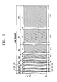
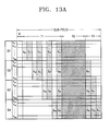
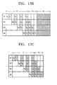
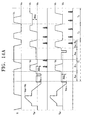
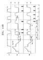
Comparing the potential levels of the sustain discharge signal shown in FIGS. 9A and 94B with those of the sustain discharge signal shown in FIG. 6, the high levels of both the sustain discharge signals are the same as VS \. However, the first low level of the sustain discharge signal of FIG. 11 is VL1 and the first low level of the sustain discharge signal of FIG. 9A is VG. Also, the second low level of the sustain discharge signal of FIG. 6 is VL2 and the second low level of the sustain discharge signal of FIG. 9A is ΔVSC. The second low level of the sustain discharge signal of FIG. 6 is VL2 and the second low level of the sustain discharge signal of FIG. 9B is ΔVSC.At this time, if a potential difference formed between the scanning electrode and the common electrode is greater than a discharge start voltage, a discharge is carried out. Otherwise, no discharge is carried out.
Claims (34)
- A display panel driving method comprising the steps of:wherein in at least one sustain period, the high level potentials of the sustain discharge signal applied to the scanning electrode are the same in all the groups and the high level potentials of the sustain discharge signal are applied at the same time to all the groups; andgrouping display cells included in scanning electrodes and common electrodes into a plurality of groups;dividing and driving a frame into a plurality of sub-fields for each group, wherein, each of the plurality of sub-fields includes an address period and a sustain period;in the address period, selecting cells to be displayed; andin the sustain period, applying high levels and low levels of a sustain discharge signal alternately to the scanning electrodes and the common electrodes so to perform a sustain discharge;
low level potentials of the sustain discharge signal applied to the scanning electrodes include a first low level potential and a second low level potential higher than the first low level potential. - The method of claim 1, wherein the first low level and the second low level potentials are applied to each of the groups at different times.
- The method of claim 1, wherein a discharge is carried out during an overlapping period of the first low level of the scanning electrode and a high level of the common electrode.
- The method of claim 1, wherein no discharge is carried out during an overlapping period of the second low level potential of the scanning electrode and the high level potential of the common electrode.
- The method of claim 1, wherein the second low level potential is equal to a potential difference between a high level potential and a low level potential of the scanning pulse applied to the scanning electrodes in the address period.
- A display panel driving method comprising the steps of:in at least one of the plurality of sub-fields, sequentially performing the address period and the sustain period to each group in a manner that:grouping display cells included in scanning electrodes and common electrodes into a plurality of groups;dividing a frame into a plurality of sub-fields for each group, wherein,each of the plurality of sub-fields includes an address period and a sustain period; andwherein in at least one sustain period, high level potentials of the sustain discharge signal applied to the scanning electrode are the same in all the groups and the high level potentials of the sustain discharge signal are applied at the same time to all the groups; anda) addressing of each group is performed and then the sustain period is performed in cells of each group subjected to addressing;b) the addressing of cells of an unaddressed group is performed after the sustain period ends for a previous group; andc) the sustain period is performed selectively in the cells of the unaddressed group subjected to addressing while the sustain period is performed in cells of that group,
low level potentials of the sustain discharge signal are applied to the scanning electrodes include a first low level potential and a second low level potential, where the second low level potential is higher than the first low level potential. - The method of claim 6, wherein the first low level and the second low level potentials are applied to each of the groups in different timings.
- The method of claim 6, wherein a discharge is carried out during an overlapping period of the first low level potential of the scanning electrode and a high level potential of the common electrode.
- The method of claim 6, wherein no discharge is carried out during an overlapping period of the second low level potential of the scanning electrode and the high level potential of the common electrode.
- The method of claim 6, wherein the second low level potential is equal to a potential difference between a high level potential and a low level potential of the scanning pulse applied to the scanning electrodes in the address period.
- The method of claim 6, wherein the sustain period further includes a common period for performing sustain discharges at the same time in all groups during a predetermined time.
- The method of claim 6, wherein the sustain period further includes a compensation period for performing an additional sustain discharge selectively for each of the groups so that each of the groups satisfies a predetermined gray-scale.
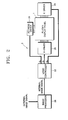
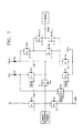
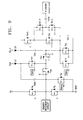
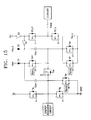
- A display panel driving apparatus which applies a scanning signal and a sustain discharge signal to a scanning electrode line of a display panel, the apparatus comprising:a first node;a sustain driving unit connected to the first node;a scanning signal high level applying unit connected to the first node;a scanning signal low level applying unit connected to the first node;a first switch, having one end connected to the scanning signal high level applying unit;a second low level applying unit, which applies a second low level of a sustain discharge signal;a second switch connected between another end of the first switch and the second low level applying unit;a high level scanning switch connected between the other end of the first switch and the scanning electrode line; anda low level scanning switch connected between the scanning electrode line and the scanning signal low level applying unit.
- The apparatus of claim 13, wherein the first switch and the second switch are toggled to each other.
- The apparatus of claim 13, wherein the sustain driving unit comprises:a high level power source for providing a high level of the sustain discharge signal;a high level switch connected between the high level source and the first node;a first low level power source for providing a first low level of the sustain discharge signal; anda low level switch connected between the first low level source of the sustain discharge signal and the first node.
- The apparatus of claim 13, wherein the scanning signal high level applying unit comprises:wherein the first switch is connected to a node located between the high level scanning source and the scanning capacitor.a high level scanning power source; anda scanning capacitor connected between the first node and the high level scanning source,
- The apparatus of claim 13, wherein the scanning signal low level applying unit comprises,
a low level scanning source; and
a control switch connected between the first node and the low level scanning source. - A computer-readable medium having embodied thereon a computer program for executing a display panel driving method, the medium comprising:wherein in at least one sustain period, the high level potentials of the sustain discharge signal applied to the scanning electrode are the same in all the groups and the high level potentials of the sustain discharge signal are applied at the same time to all the groups; andcode for grouping display cells included in scanning electrodes and common electrodes into a plurality of groups;code for dividing and driving a frame into a plurality of sub-fields for each group, wherein, each of the plurality of sub-fields includes an address period and a sustain period;code for, in the address period, selecting cells to be displayed; andcode for, in the sustain period, applying high levels and low levels of a sustain discharge signal alternately to the scanning electrodes and the common electrodes so to perform a sustain discharge;
low level potentials of the sustain discharge signal applied to the scanning electrodes include a first low level potential and a second low level potential higher than the first low level potential. - The medium of claim 18, wherein the first low level and the second low level potentials are applied to each of the groups at different times.
- The medium of claim 18, wherein a discharge is carried out during an overlapping period of the first low level of the scanning electrode and a high level of the common electrode.
- The medium of claim 18, wherein no discharge is carried out during an overlapping period of the second low level potential of the scanning electrode and the high level potential of the common electrode.
- The medium of claim 18, wherein the second low level potential is equal to a potential difference between a high level potential and a low level potential of the scanning pulse applied to the scanning electrodes in the address period.
- A computer-readable medium having embodied thereon a computer program for executing a display panel driving method, the medium comprising:wherein in at least one sustain period, high level potentials of the sustain discharge signal applied to the scanning electrode are the same in all the groups and the high level potentials of the sustain discharge signal are applied at the same time to all the groups; andcode for grouping display cells included in scanning electrodes and common electrodes into a plurality of groups;code for dividing a frame into a plurality of sub-fields for each group, wherein,each of the plurality of sub-fields includes an address period and a sustain period; andcode for, in at least one of the plurality of sub-fields, sequentially performing the address period and the sustain period to each group in a manner that:a) addressing of each group is performed and then the sustain period is performed in cells of each group subjected to addressing;b) addressing of cells of a different group is performed after the sustain period ends; andc) the sustain period is performed selectively in the cells of the different group subjected to addressing while the sustain period is performed in cells of a group,
low level potentials of the sustain discharge signal are applied to the scanning electrodes include a first low level potential and a second low level potential, where the second low level potential is higher than the first low level potential. - The medium of claim 23, wherein the first low level and the second low level potentials are applied to each of the groups in different timings.
- The medium of claim 23, wherein a discharge is carried out during an overlapping period of the first low level potential of the scanning electrode and a high level potential of the common electrode.
- The medium of claim 23, wherein no discharge is carried out during an overlapping period of the second low level potential of the scanning electrode and the high level potential of the common electrode.
- The medium of claim 23, wherein the second low level potential is equal to a potential difference between a high level potential and a low level potential of the scanning pulse applied to the scanning electrodes in the address period.
- The medium of claim 23, wherein the sustain period further includes a common period for performing sustain discharges at the same time in all groups during a predetermined time.
- A display panel driving apparatus which applies a scanning signal and a sustain discharge signal to a scanning electrode line of a display panel, the apparatus comprising:a first mode;a means for driving a sustain signal connected to the first mode;a means for apply a high level scanning signal connected to the first mode;a means for applying a low level scanning signal connected to the first mode;a means for switching having one end connected to the means for applying a high level scanning signal;a means for applying a low level scanning discharge signal;a second means for switching connected between another end of the first means for switching and the means for applying a low level scanning discharge signal;a third means for switching connected between another end of the first means for switching and the scanning electrode line; anda fourth means for switching connected between the scanning electrode line and the means for applying the low level scanning signal.
- A display panel driving method comprising the steps of:in the address period, selecting cells to be displayed; anddriving a frame into a plurality of sub-fields, wherein, each of the plurality of sub-fields includes an address period and a sustain period;
in the sustain period, applying high levels and low levels of a sustain discharge signal alternately to scanning electrodes and common electrodes so to perform a sustain discharge;
wherein in at least one sustain period, the high level potentials of the sustain discharge signal applied to the scanning electrode are the same and the high level potentials of the sustain discharge signal are applied at the same time; and
low level potentials of the sustain discharge signal applied to the scanning electrodes include a first low level potential and a second low level potential higher than the first low level potential. - The method of claim 30, wherein the first low level and the second low level potentials are applied at different times.
- The method of claim 30, wherein a discharge is carried out during an overlapping period of the first low level of the scanning electrode and a high level of the common electrode.
- The method of claim 30, wherein no discharge is carried out during an overlapping period of the second low level potential of the scanning electrode and the high level potential of the common electrode.
- The method of claim 30, wherein the second low level potential is equal to a potential difference between a high level potential and a low level potential of the scanning pulse applied to the scanning electrodes in the address period.
Applications Claiming Priority (2)
| Application Number | Priority Date | Filing Date | Title |
|---|---|---|---|
| KR1020040021551A KR100509609B1 (en) | 2004-03-30 | 2004-03-30 | Method and apparatus for display panel |
| KR2004021551 | 2004-03-30 |
Publications (2)
| Publication Number | Publication Date |
|---|---|
| EP1585095A2 true EP1585095A2 (en) | 2005-10-12 |
| EP1585095A3 EP1585095A3 (en) | 2008-03-12 |
Family
ID=34910079
Family Applications (1)
| Application Number | Title | Priority Date | Filing Date |
|---|---|---|---|
| EP05075346A Withdrawn EP1585095A3 (en) | 2004-03-30 | 2005-02-09 | Method and apparatus for driving display panel |
Country Status (5)
| Country | Link |
|---|---|
| US (1) | US20050219157A1 (en) |
| EP (1) | EP1585095A3 (en) |
| JP (1) | JP4188898B2 (en) |
| KR (1) | KR100509609B1 (en) |
| CN (1) | CN1677461A (en) |
Cited By (1)
| Publication number | Priority date | Publication date | Assignee | Title |
|---|---|---|---|---|
| EP1801771A1 (en) * | 2005-12-21 | 2007-06-27 | Samsung SDI Co., Ltd. | Apparatus and method for driving display panel |
Families Citing this family (8)
| Publication number | Priority date | Publication date | Assignee | Title |
|---|---|---|---|---|
| KR100719597B1 (en) * | 2006-02-07 | 2007-05-17 | 삼성에스디아이 주식회사 | Driving method of plasma display panel |
| US7719491B2 (en) * | 2006-02-13 | 2010-05-18 | Chunghwa Picture Tubes, Ltd. | Method for driving a plasma display panel |
| KR100740094B1 (en) | 2006-02-28 | 2007-07-16 | 삼성에스디아이 주식회사 | Plasma display device and driving method thereof |
| KR100786876B1 (en) | 2006-12-27 | 2007-12-20 | 삼성에스디아이 주식회사 | Plasma display and driving method thereof |
| WO2008090700A1 (en) * | 2007-01-24 | 2008-07-31 | Panasonic Corporation | Plasma display panel drive circuit and plasma display device |
| KR100908719B1 (en) * | 2007-03-13 | 2009-07-22 | 삼성에스디아이 주식회사 | Plasma Display and Driving Device |
| KR100839386B1 (en) * | 2007-03-26 | 2008-06-20 | 삼성에스디아이 주식회사 | Plasma display and driving method thereof |
| CN107818760B (en) * | 2016-09-14 | 2019-11-19 | 上海和辉光电有限公司 | Display methods, display panel and the display device of display device |
Citations (4)
| Publication number | Priority date | Publication date | Assignee | Title |
|---|---|---|---|---|
| US5670974A (en) | 1994-09-28 | 1997-09-23 | Nec Corporation | Energy recovery driver for a dot matrix AC plasma display panel with a parallel resonant circuit allowing power reduction |
| US5684499A (en) | 1993-11-29 | 1997-11-04 | Nec Corporation | Method of driving plasma display panel having improved operational margin |
| US6710755B1 (en) | 1999-10-12 | 2004-03-23 | Pioneer Corporation | Method for driving plasma display panel |
| EP1424677A2 (en) | 2002-11-26 | 2004-06-02 | Samsung SDI Co., Ltd. | Method and apparatus for driving plasma panels by performing mixed address period and sustain period |
Family Cites Families (7)
| Publication number | Priority date | Publication date | Assignee | Title |
|---|---|---|---|---|
| US4866349A (en) * | 1986-09-25 | 1989-09-12 | The Board Of Trustees Of The University Of Illinois | Power efficient sustain drivers and address drivers for plasma panel |
| JP3259253B2 (en) * | 1990-11-28 | 2002-02-25 | 富士通株式会社 | Gray scale driving method and gray scale driving apparatus for flat display device |
| JP3499058B2 (en) * | 1995-09-13 | 2004-02-23 | 富士通株式会社 | Driving method of plasma display and plasma display device |
| US6262160B1 (en) * | 1999-02-10 | 2001-07-17 | Nippon Bee Chemical Co., Ltd | Water base adhesion promotor for polypropylene and method for coating to polypropylene materials using the promotor |
| EP1172787A1 (en) * | 2000-07-13 | 2002-01-16 | Deutsche Thomson-Brandt Gmbh | Gradation control of a matrix display |
| JP4945033B2 (en) * | 2001-06-27 | 2012-06-06 | 日立プラズマディスプレイ株式会社 | Plasma display device |
| US6903515B2 (en) * | 2002-06-21 | 2005-06-07 | Lg Electronics Inc. | Sustain driving apparatus and method for plasma display panel |
-
2004
- 2004-03-30 KR KR1020040021551A patent/KR100509609B1/en not_active IP Right Cessation
- 2004-09-30 JP JP2004288334A patent/JP4188898B2/en not_active Expired - Fee Related
-
2005
- 2005-01-07 US US11/030,202 patent/US20050219157A1/en not_active Abandoned
- 2005-02-09 EP EP05075346A patent/EP1585095A3/en not_active Withdrawn
- 2005-02-21 CN CNA2005100526018A patent/CN1677461A/en active Pending
Patent Citations (4)
| Publication number | Priority date | Publication date | Assignee | Title |
|---|---|---|---|---|
| US5684499A (en) | 1993-11-29 | 1997-11-04 | Nec Corporation | Method of driving plasma display panel having improved operational margin |
| US5670974A (en) | 1994-09-28 | 1997-09-23 | Nec Corporation | Energy recovery driver for a dot matrix AC plasma display panel with a parallel resonant circuit allowing power reduction |
| US6710755B1 (en) | 1999-10-12 | 2004-03-23 | Pioneer Corporation | Method for driving plasma display panel |
| EP1424677A2 (en) | 2002-11-26 | 2004-06-02 | Samsung SDI Co., Ltd. | Method and apparatus for driving plasma panels by performing mixed address period and sustain period |
Cited By (1)
| Publication number | Priority date | Publication date | Assignee | Title |
|---|---|---|---|---|
| EP1801771A1 (en) * | 2005-12-21 | 2007-06-27 | Samsung SDI Co., Ltd. | Apparatus and method for driving display panel |
Also Published As
| Publication number | Publication date |
|---|---|
| EP1585095A3 (en) | 2008-03-12 |
| CN1677461A (en) | 2005-10-05 |
| JP4188898B2 (en) | 2008-12-03 |
| KR100509609B1 (en) | 2005-08-22 |
| JP2005284249A (en) | 2005-10-13 |
| US20050219157A1 (en) | 2005-10-06 |
Similar Documents
| Publication | Publication Date | Title |
|---|---|---|
| JP3511475B2 (en) | Display panel driving method and integrated circuit device | |
| KR100354678B1 (en) | Drive method of plasma display and drive device thereof | |
| EP1585095A2 (en) | Method and apparatus for driving display panel | |
| JPH09311661A (en) | Plasma display panel driving method and plasma display apparatus employing the same | |
| KR19980079336A (en) | Plasma Display Panel, Plasma Display Device and Plasma Display Panel Driving Method | |
| JP2002215086A (en) | Method for driving plasma display device, and plasma display device | |
| JP2004029412A (en) | Method of driving plasma display panel | |
| KR100626017B1 (en) | Method of driving plasma a display panel and driver thereof | |
| KR100774875B1 (en) | Driving Method for Plasma Display Panel | |
| KR100524306B1 (en) | Reset method and apparatus of plasma display panel | |
| KR100627416B1 (en) | Driving method of plasma display device | |
| KR100680709B1 (en) | Driving Device for Plasma Display Panel | |
| JP2002023689A (en) | Plasma display device | |
| JP4198125B2 (en) | Plasma display device | |
| KR100524311B1 (en) | Method and apparatus for driving plasma display panel | |
| JP2002108278A (en) | Plasma display device and driving method therefor | |
| KR100747169B1 (en) | Plasma Display Apparatus and Driving Method for Plasma Display Apparatus | |
| KR20060091202A (en) | Apparatus for driving plasma display panel | |
| KR100524304B1 (en) | Method and apparatus driving of plasma display panel | |
| KR100740109B1 (en) | Driving method of plasma display | |
| KR100631122B1 (en) | Plasma display and driving method thereof | |
| KR100667321B1 (en) | Plasma display apparatus and driving method thereof | |
| KR100646319B1 (en) | Plasma Display Apparatus and Driving Method thereof | |
| KR100667558B1 (en) | Plasma Display Apparatus and Driving Method of the Same | |
| KR100778506B1 (en) | Plasma display device and driving method thereof |
Legal Events
| Date | Code | Title | Description |
|---|---|---|---|
| PUAI | Public reference made under article 153(3) epc to a published international application that has entered the european phase |
Free format text: ORIGINAL CODE: 0009012 |
|
| AK | Designated contracting states |
Kind code of ref document: A2 Designated state(s): AT BE BG CH CY CZ DE DK EE ES FI FR GB GR HU IE IS IT LI LT LU MC NL PL PT RO SE SI SK TR |
|
| AX | Request for extension of the european patent |
Extension state: AL BA HR LV MK YU |
|
| RIN1 | Information on inventor provided before grant (corrected) |
Inventor name: LEE, JOO-YULLEGAL & IP TEAM, SAMSUNG SDI CO. L |
|
| PUAL | Search report despatched |
Free format text: ORIGINAL CODE: 0009013 |
|
| AK | Designated contracting states |
Kind code of ref document: A3 Designated state(s): AT BE BG CH CY CZ DE DK EE ES FI FR GB GR HU IE IS IT LI LT LU MC NL PL PT RO SE SI SK TR |
|
| AX | Request for extension of the european patent |
Extension state: AL BA HR LV MK YU |
|
| 17P | Request for examination filed |
Effective date: 20080905 |
|
| AKX | Designation fees paid |
Designated state(s): DE FR GB IT NL |
|
| STAA | Information on the status of an ep patent application or granted ep patent |
Free format text: STATUS: THE APPLICATION HAS BEEN WITHDRAWN |
|
| 18W | Application withdrawn |
Effective date: 20091019 |