EP1580890A1 - Treiber für eine niedrige Betriebsspannung - Google Patents
Treiber für eine niedrige Betriebsspannung Download PDFInfo
- Publication number
- EP1580890A1 EP1580890A1 EP05447057A EP05447057A EP1580890A1 EP 1580890 A1 EP1580890 A1 EP 1580890A1 EP 05447057 A EP05447057 A EP 05447057A EP 05447057 A EP05447057 A EP 05447057A EP 1580890 A1 EP1580890 A1 EP 1580890A1
- Authority
- EP
- European Patent Office
- Prior art keywords
- switch
- voltage
- driver circuit
- feedback arrangement
- current
- Prior art date
- Legal status (The legal status is an assumption and is not a legal conclusion. Google has not performed a legal analysis and makes no representation as to the accuracy of the status listed.)
- Granted
Links
- 238000005516 engineering process Methods 0.000 claims abstract description 11
- 239000003990 capacitor Substances 0.000 claims description 8
- XUIMIQQOPSSXEZ-UHFFFAOYSA-N Silicon Chemical compound [Si] XUIMIQQOPSSXEZ-UHFFFAOYSA-N 0.000 description 3
- 230000008859 change Effects 0.000 description 3
- 230000000630 rising effect Effects 0.000 description 3
- 229910052710 silicon Inorganic materials 0.000 description 3
- 239000010703 silicon Substances 0.000 description 3
- 230000001052 transient effect Effects 0.000 description 3
- 238000010586 diagram Methods 0.000 description 2
- 230000008713 feedback mechanism Effects 0.000 description 2
- 230000007246 mechanism Effects 0.000 description 2
- 238000000034 method Methods 0.000 description 2
- 238000004088 simulation Methods 0.000 description 2
- 230000009471 action Effects 0.000 description 1
- 230000008901 benefit Effects 0.000 description 1
- 230000015556 catabolic process Effects 0.000 description 1
- 230000003247 decreasing effect Effects 0.000 description 1
- 230000009977 dual effect Effects 0.000 description 1
- 230000001939 inductive effect Effects 0.000 description 1
- 239000002184 metal Substances 0.000 description 1
- 238000012544 monitoring process Methods 0.000 description 1
- 230000003071 parasitic effect Effects 0.000 description 1
- 230000003449 preventive effect Effects 0.000 description 1
- 230000008569 process Effects 0.000 description 1
- 230000009897 systematic effect Effects 0.000 description 1
- 230000007704 transition Effects 0.000 description 1
- 230000001960 triggered effect Effects 0.000 description 1
Images

Classifications
-
- H—ELECTRICITY
- H03—ELECTRONIC CIRCUITRY
- H03K—PULSE TECHNIQUE
- H03K19/00—Logic circuits, i.e. having at least two inputs acting on one output; Inverting circuits
- H03K19/003—Modifications for increasing the reliability for protection
- H03K19/00315—Modifications for increasing the reliability for protection in field-effect transistor circuits
-
- H—ELECTRICITY
- H03—ELECTRONIC CIRCUITRY
- H03K—PULSE TECHNIQUE
- H03K19/00—Logic circuits, i.e. having at least two inputs acting on one output; Inverting circuits
- H03K19/0175—Coupling arrangements; Interface arrangements
- H03K19/0185—Coupling arrangements; Interface arrangements using field effect transistors only
- H03K19/018507—Interface arrangements
Definitions
- the present invention is related to a low voltage driver circuit.
- a low voltage driver implemented as an open drain output essentially contains just a switch to ground. This switch can be either on or off.
- the load is a coil (which is the driving coil of a relais).
- a flyback mechanism must be implemented to control the behaviour (i.e. to control the pin voltage).
- EP 0627818 a circuit for reducing the transition delay of an output power transistor is disclosed.
- the integrating stage controlling the slew rate is not able to keep the output voltage below a predefined maximum.
- Neither patent document US2002/0181180 A1 relating to an over-current protection circuit, is suited for keeping the voltage range within a given range.
- the present invention aims to provide a low voltage driver, implemented in a low-voltage CMOS, technology that provides flyback protection, over-current protection and slope control.
- the invention relates to a driver circuit comprising an input, an output and at least one low-ohmic switch.
- This switch is provided with an input terminal and two output terminals.
- the driver circuit further comprises a first feedback arrangement in a low-voltage CMOS technology, inputting the voltage of one output terminal of the switch. Said first feedback arrangement steers the input terminal of said switch to keep the voltage of said one output terminal within a predefined range, which is characterised by a threshold value.
- the first feedback arrangement is operative only when the voltage of said one output terminal reaches said threshold value.
- the first feedback arrangement advantageously comprises an active component.
- the first feedback arrangement comprises an asymmetric operational amplifier, whereby a first input of the operational amplifier is connected to the voltage of said one output terminal and whereby the output of the operational amplifier steers the input terminal of the switch.
- the first feedback arrangement comprises means for providing a voltage reference, which is used for setting said threshold value.
- said means are connected to a second input of the operational amplifier.
- the low-ohmic switch preferably is made in a low-voltage CMOS technology.
- the driver circuit further comprises a second feedback arrangement inputting the voltage of the one output terminal of the switch and steering the input terminal of the switch to keep the voltage slope at the output terminal in absolute value below a predefined maximum.
- the second feedback arrangement typically is passive. It can for example comprise a capacitor.
- the second feedback arrangement further comprises a resistor.
- a current source can perform the function of loading the capacitor.
- the driver circuit further comprises a third feedback arrangement steering the input terminal of the switch to keep the current through the switch within a predefined range.
- the third feedback arrangement further comprises a logical circuit driving the input terminal of the switch into a low-current state when the driver circuit input and the voltage of the one output terminal indicate a current through said switch outside said predefined range.
- the latter 'and' is to be understood as a logical 'and'.
- the third feedback arrangement reuses the above-mentioned resistor.
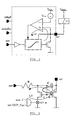
- Fig. 1 represents a general block diagram of a low voltage driver according to the invention.
- Fig. 2 represents a scheme showing the over-current protection principle.
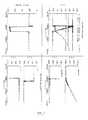
- Fig. 3 represents some simulation results showing the driver behaviour in case it is switched on.
- Fig. 4 represents some simulation results showing the driver behaviour in case it is switched off.
- the current through the driver is mainly set by the coil (11) series resistance R L .
- the switch-on resistance R S including all pin-to-pin parasitic series resistances, is significantly less than R L .
- the driver circuit performs a slope control function.
- a maximum pin voltage slope is required in order to limit the generated EMI (ElectroMagnetic Interference).
- the pin voltage slope further provides the advantage that, as it is finite, it leaves some time for the flyback feedback circuit to become active when the switch is switched off.
- the voltage slope at pin out (in absolute value) is kept below said maximum, independently of the applied load.
- the pin voltage slope is realised in the following way.
- a capacitance C is put between the drain (this is the pin or the driver output) and the switch transistor gate.
- a series resistance R is inserted between the transistor gate and the driving (digital) buffer.
- the drain voltage i.e. the pin
- the drain voltage can only change with a rate that is equal to the rate with which the capacitor's voltage changes, and this change is set by the current through the resistor R and charging the capacitor C.
- the circuit of Fig.2 comprises a capacitive voltage feedback mechanism from drain to gate. E.g., when the switch goes off, the pin voltage will rise, driven by the free-wheeling coil. But due to the capacitor this will also pull up the gate of the switch, again switching on the switch. This will counter the pin voltage rise.
- a negative feedback mechanism This constitutes a feedback loop L2 (see Fig.2).
- the pin voltage can only change when the voltage across the capacitor C changes.
- the pin slope (in V/s) equals I/C, I being the current through the resistor and flowing into (i.e. charging) the feedback capacitor C.
- I is equal to V/R, V being the voltage across the gate series resistor R.
- I L current I L of 30 mA
- the driver also needs an over-current protection (OCP). Indeed, when the switch is on and the output pin is shorted to V DD , excessive current and power can result (potentially damaging the chip) if no preventive measures are taken.
- OCP over-current protection
- OCP_I over-current limit
- Fig. 2 schematically shows the principle. One recognises the two ' aan equals 1' states:
- OCP_V TH should not be set too low: in the normal-on state with a coil as load, the pin (DC) voltage should never reach this threshold. In a worst case the pin DC voltage can be rather high.
- the AND gate in Fig.2 is not required. This condition for enabling the OCP_sw switch is required for the following reason. Suppose a coil is connected and the driver goes off (and there are no shorts). The pin voltage will rise fast (but slope-controlled) to V DD and the current will decay slowly. Hence a big current and a high pin voltage will, temporarily, result. This is just as if there were over-current (or better, over-power). But this is normal and has to be like that, as this situation does not last long. Without the ' aan equals 1' condition, the OCP circuit would be activated. However, limiting the switch current is certainly not allowed during this transient.
- the OCP circuit would even compete with the flyback circuit (which keeps the coil current flowing through the switch during this transient). With the condition included: because aan is '0', the OCP circuit will not (and should not) be triggered. The condition hence is required to avoid problems during normal transient. Or a different, but equivalent view: aan acts immediately through the AND, while action through the resistor R and the flyback circuit would take a significant time.
- the lower-right graph of Fig.4 shows the AND inputs.
- the switch is loaded with the external coil.
- the switch goes off, the coil will free-wheel.
- the pin voltage rises, the pin capacitance being charged by current delivered by the coil.
- pin voltage slope control is built in.
- the switch will not abruptly go off, it will still take some of the coil current and hence the pin voltage will rise less fast.
- the pin voltage will surpass V DD .
- the voltage will go on rising until a mechanism is encountered that stops the increase. If nothing is done, this will be at voltage breakdown of the weakest structure. Clearly this must be avoided or, better, this has to happen in a controlled way.
- the coil current itself will start to decrease as soon as the pin voltage starts to rise. However, the current will not at all have been decreased to zero when the pin voltage surpasses V DD .
- the purpose of the implemented flyback circuit is to limit the pin voltage to V DD +V FB , V DD being the on-chip supply and V FB a controlled voltage value (see Fig.1).
- V FB is on the order of 100 mV. It has to be that low in order to limit the pin voltage to a value slightly above V DD . Indeed, the maximum supply for this design turns out to be equal to the silicon technology maximum (which of course is no coincidence). A 100 mV violation however is to be acceptable. Note that the flyback feedback loop L1 is much more sensitive than that for the overcurrent protection.
- V DD + V FB the switch is again activated, sinking the coil current and by doing so stopping the pin voltage rise.
- the loop actually will regulate the pin voltage to be equal to (V DD + V FB ).
- V FB is actually implemented by giving the opamp a systematic offset (which is equal to V FB ).
- V FB hence does not exist explicitly.
- the opamp (see Fig.1) has the important feature that when the pin voltage is lower than (V DD + V FB ), the feedback loop is open, i.e. the loop will not try to put the switch off when he is to be on.
- V FB is rather small, typical value is 100 mV.
- ⁇ L the discharge occurs with a time constant ⁇ L . If V FB had been higher, the discharge occurs with the same ⁇ L but the zero current state would be reached significantly faster.
- V DDR this is the external V DD to which the relais are connected (see Fig.1), should not be more than V FB Volt higher than the chip V DD . Otherwise, in the switch off, zero current state the flyback circuit would activate the switch in order to try to lower the pin voltage. Some margin is taken with respect to the absolute maximum, which is V FB . For the same reason, a dedicated (i.e. only used for that purpose) on-chip metal track is used to connect the chip V DD pad (or pin) to the inputs of the flyback opamp.
Landscapes
- Engineering & Computer Science (AREA)
- Computer Hardware Design (AREA)
- Physics & Mathematics (AREA)
- Computing Systems (AREA)
- General Engineering & Computer Science (AREA)
- Mathematical Physics (AREA)
- Electronic Switches (AREA)
Priority Applications (1)
| Application Number | Priority Date | Filing Date | Title |
|---|---|---|---|
| EP05447057A EP1580890B1 (de) | 2004-03-18 | 2005-03-18 | Treiber für eine niedrige Betriebsspannung |
Applications Claiming Priority (3)
| Application Number | Priority Date | Filing Date | Title |
|---|---|---|---|
| EP04447067 | 2004-03-18 | ||
| EP04447067A EP1578018A1 (de) | 2004-03-18 | 2004-03-18 | Treiber für eine niedrige Betriebsspannung |
| EP05447057A EP1580890B1 (de) | 2004-03-18 | 2005-03-18 | Treiber für eine niedrige Betriebsspannung |
Publications (2)
| Publication Number | Publication Date |
|---|---|
| EP1580890A1 true EP1580890A1 (de) | 2005-09-28 |
| EP1580890B1 EP1580890B1 (de) | 2007-05-09 |
Family
ID=34863135
Family Applications (1)
| Application Number | Title | Priority Date | Filing Date |
|---|---|---|---|
| EP05447057A Expired - Lifetime EP1580890B1 (de) | 2004-03-18 | 2005-03-18 | Treiber für eine niedrige Betriebsspannung |
Country Status (1)
| Country | Link |
|---|---|
| EP (1) | EP1580890B1 (de) |
Citations (4)
| Publication number | Priority date | Publication date | Assignee | Title |
|---|---|---|---|---|
| US4622482A (en) * | 1985-08-30 | 1986-11-11 | Motorola, Inc. | Slew rate limited driver circuit which minimizes crossover distortion |
| EP0627818A1 (de) * | 1993-05-31 | 1994-12-07 | STMicroelectronics S.r.l. | Verringerung der Übergangszeit eines Ausgangsleistungstransistors |
| US6281730B1 (en) * | 1999-05-13 | 2001-08-28 | National Semiconductor Corporation | Controlled slew rate driver |
| US20020181180A1 (en) * | 2001-04-19 | 2002-12-05 | Texas Instruments Incorporated | Over-current protection circuit and method |
-
2005
- 2005-03-18 EP EP05447057A patent/EP1580890B1/de not_active Expired - Lifetime
Patent Citations (4)
| Publication number | Priority date | Publication date | Assignee | Title |
|---|---|---|---|---|
| US4622482A (en) * | 1985-08-30 | 1986-11-11 | Motorola, Inc. | Slew rate limited driver circuit which minimizes crossover distortion |
| EP0627818A1 (de) * | 1993-05-31 | 1994-12-07 | STMicroelectronics S.r.l. | Verringerung der Übergangszeit eines Ausgangsleistungstransistors |
| US6281730B1 (en) * | 1999-05-13 | 2001-08-28 | National Semiconductor Corporation | Controlled slew rate driver |
| US20020181180A1 (en) * | 2001-04-19 | 2002-12-05 | Texas Instruments Incorporated | Over-current protection circuit and method |
Also Published As
| Publication number | Publication date |
|---|---|
| EP1580890B1 (de) | 2007-05-09 |
Similar Documents
| Publication | Publication Date | Title |
|---|---|---|
| TWI568179B (zh) | 高壓閘極驅動電路 | |
| US7276888B2 (en) | Precharge circuit for DC/DC boost converter startup | |
| US6542344B1 (en) | Switching regulator | |
| JP5135214B2 (ja) | ソフトスタート回路を備えた突入電流制御システムおよび方法 | |
| US20090154035A1 (en) | ESD Protection Circuit | |
| WO2007074828A1 (ja) | 電力供給制御装置及びその閾値変更方法 | |
| EP4441893B1 (de) | Gate-treiber für grosse spannungen mit transistoren mit niedrigem gate-oxid-gehalt | |
| US6373296B1 (en) | Circuit configuration for driving a semiconductor switch | |
| US12231032B2 (en) | Pass gate driver | |
| US12155376B2 (en) | Driver discharge circuit | |
| JP7518247B2 (ja) | 出力トランジスタの駆動回路、半導体装置、自動車 | |
| US20100014202A1 (en) | Control Circuit for a Power Field-Effect Transistor and Method for Configuring a Control Circuit for a Power Field-Effect Transistor | |
| EP1580890B1 (de) | Treiber für eine niedrige Betriebsspannung | |
| US11196243B2 (en) | Pin-short detection circuits | |
| EP1578018A1 (de) | Treiber für eine niedrige Betriebsspannung | |
| US20230308089A1 (en) | High-side semiconductor switch with over-current protection | |
| CN119866594A (zh) | 切换电压转换器中的反向恢复保护 | |
| CN100426502C (zh) | 形成半导体器件及其结构的方法 | |
| CN114115408A (zh) | 调节器用半导体集成电路 | |
| WO2002084874A1 (en) | A multiple-stage control circuit to control rush current in a mosfet load switch | |
| US7994759B2 (en) | System and method for driving a power supply device in an initial activation stage | |
| US7994767B2 (en) | Control device for transient recovery of DC-DC converters | |
| US12273099B2 (en) | Driver with adaptive drive strength | |
| US20240364337A1 (en) | Excessive current protection for bootstrap capacitor charging | |
| US12149236B2 (en) | Pre-biased dual current sensing |
Legal Events
| Date | Code | Title | Description |
|---|---|---|---|
| PUAI | Public reference made under article 153(3) epc to a published international application that has entered the european phase |
Free format text: ORIGINAL CODE: 0009012 |
|
| AK | Designated contracting states |
Kind code of ref document: A1 Designated state(s): AT BE BG CH CY CZ DE DK EE ES FI FR GB GR HU IE IS IT LI LT LU MC NL PL PT RO SE SI SK TR |
|
| AX | Request for extension of the european patent |
Extension state: AL BA HR LV MK YU |
|
| 17P | Request for examination filed |
Effective date: 20051107 |
|
| AKX | Designation fees paid |
Designated state(s): AT BE BG CH CY CZ DE DK EE ES FI FR GB GR HU IE IS IT LI LT LU MC NL PL PT RO SE SI SK TR |
|
| GRAP | Despatch of communication of intention to grant a patent |
Free format text: ORIGINAL CODE: EPIDOSNIGR1 |
|
| GRAS | Grant fee paid |
Free format text: ORIGINAL CODE: EPIDOSNIGR3 |
|
| GRAA | (expected) grant |
Free format text: ORIGINAL CODE: 0009210 |
|
| AK | Designated contracting states |
Kind code of ref document: B1 Designated state(s): AT BE BG CH CY CZ DE DK EE ES FI FR GB GR HU IE IS IT LI LT LU MC NL PL PT RO SE SI SK TR |
|
| PG25 | Lapsed in a contracting state [announced via postgrant information from national office to epo] |
Ref country code: FI Free format text: LAPSE BECAUSE OF FAILURE TO SUBMIT A TRANSLATION OF THE DESCRIPTION OR TO PAY THE FEE WITHIN THE PRESCRIBED TIME-LIMIT Effective date: 20070509 Ref country code: CH Free format text: LAPSE BECAUSE OF FAILURE TO SUBMIT A TRANSLATION OF THE DESCRIPTION OR TO PAY THE FEE WITHIN THE PRESCRIBED TIME-LIMIT Effective date: 20070509 Ref country code: LI Free format text: LAPSE BECAUSE OF FAILURE TO SUBMIT A TRANSLATION OF THE DESCRIPTION OR TO PAY THE FEE WITHIN THE PRESCRIBED TIME-LIMIT Effective date: 20070509 |
|
| REG | Reference to a national code |
Ref country code: GB Ref legal event code: FG4D |
|
| REG | Reference to a national code |
Ref country code: CH Ref legal event code: EP |
|
| REG | Reference to a national code |
Ref country code: IE Ref legal event code: FG4D |
|
| REF | Corresponds to: |
Ref document number: 602005001071 Country of ref document: DE Date of ref document: 20070621 Kind code of ref document: P |
|
| PG25 | Lapsed in a contracting state [announced via postgrant information from national office to epo] |
Ref country code: SE Free format text: LAPSE BECAUSE OF FAILURE TO SUBMIT A TRANSLATION OF THE DESCRIPTION OR TO PAY THE FEE WITHIN THE PRESCRIBED TIME-LIMIT Effective date: 20070809 |
|
| PG25 | Lapsed in a contracting state [announced via postgrant information from national office to epo] |
Ref country code: ES Free format text: LAPSE BECAUSE OF FAILURE TO SUBMIT A TRANSLATION OF THE DESCRIPTION OR TO PAY THE FEE WITHIN THE PRESCRIBED TIME-LIMIT Effective date: 20070820 |
|
| RAP2 | Party data changed (patent owner data changed or rights of a patent transferred) |
Owner name: LEA ABC Owner name: INTERUNIVERSITAIR MICROELEKTRONICA CENTRUM ( IMEC) |
|
| PG25 | Lapsed in a contracting state [announced via postgrant information from national office to epo] |
Ref country code: IS Free format text: LAPSE BECAUSE OF FAILURE TO SUBMIT A TRANSLATION OF THE DESCRIPTION OR TO PAY THE FEE WITHIN THE PRESCRIBED TIME-LIMIT Effective date: 20070909 |
|
| NLT2 | Nl: modifications (of names), taken from the european patent patent bulletin |
Owner name: INTERUNIVERSITAIR MICROELEKTRONICA CENTRUM ( IMEC) Effective date: 20070829 |
|
| NLV1 | Nl: lapsed or annulled due to failure to fulfill the requirements of art. 29p and 29m of the patents act | ||
| REG | Reference to a national code |
Ref country code: CH Ref legal event code: PL |
|
| ET | Fr: translation filed | ||
| PG25 | Lapsed in a contracting state [announced via postgrant information from national office to epo] |
Ref country code: PL Free format text: LAPSE BECAUSE OF FAILURE TO SUBMIT A TRANSLATION OF THE DESCRIPTION OR TO PAY THE FEE WITHIN THE PRESCRIBED TIME-LIMIT Effective date: 20070509 Ref country code: AT Free format text: LAPSE BECAUSE OF FAILURE TO SUBMIT A TRANSLATION OF THE DESCRIPTION OR TO PAY THE FEE WITHIN THE PRESCRIBED TIME-LIMIT Effective date: 20070509 |
|
| PG25 | Lapsed in a contracting state [announced via postgrant information from national office to epo] |
Ref country code: BE Free format text: LAPSE BECAUSE OF FAILURE TO SUBMIT A TRANSLATION OF THE DESCRIPTION OR TO PAY THE FEE WITHIN THE PRESCRIBED TIME-LIMIT Effective date: 20070509 |
|
| PG25 | Lapsed in a contracting state [announced via postgrant information from national office to epo] |
Ref country code: BG Free format text: LAPSE BECAUSE OF FAILURE TO SUBMIT A TRANSLATION OF THE DESCRIPTION OR TO PAY THE FEE WITHIN THE PRESCRIBED TIME-LIMIT Effective date: 20070809 Ref country code: DK Free format text: LAPSE BECAUSE OF FAILURE TO SUBMIT A TRANSLATION OF THE DESCRIPTION OR TO PAY THE FEE WITHIN THE PRESCRIBED TIME-LIMIT Effective date: 20070509 Ref country code: NL Free format text: LAPSE BECAUSE OF FAILURE TO SUBMIT A TRANSLATION OF THE DESCRIPTION OR TO PAY THE FEE WITHIN THE PRESCRIBED TIME-LIMIT Effective date: 20070509 Ref country code: PT Free format text: LAPSE BECAUSE OF FAILURE TO SUBMIT A TRANSLATION OF THE DESCRIPTION OR TO PAY THE FEE WITHIN THE PRESCRIBED TIME-LIMIT Effective date: 20071009 Ref country code: SI Free format text: LAPSE BECAUSE OF FAILURE TO SUBMIT A TRANSLATION OF THE DESCRIPTION OR TO PAY THE FEE WITHIN THE PRESCRIBED TIME-LIMIT Effective date: 20070509 Ref country code: CZ Free format text: LAPSE BECAUSE OF FAILURE TO SUBMIT A TRANSLATION OF THE DESCRIPTION OR TO PAY THE FEE WITHIN THE PRESCRIBED TIME-LIMIT Effective date: 20070509 |
|
| PG25 | Lapsed in a contracting state [announced via postgrant information from national office to epo] |
Ref country code: LT Free format text: LAPSE BECAUSE OF FAILURE TO SUBMIT A TRANSLATION OF THE DESCRIPTION OR TO PAY THE FEE WITHIN THE PRESCRIBED TIME-LIMIT Effective date: 20070509 Ref country code: SK Free format text: LAPSE BECAUSE OF FAILURE TO SUBMIT A TRANSLATION OF THE DESCRIPTION OR TO PAY THE FEE WITHIN THE PRESCRIBED TIME-LIMIT Effective date: 20070509 |
|
| PLBE | No opposition filed within time limit |
Free format text: ORIGINAL CODE: 0009261 |
|
| STAA | Information on the status of an ep patent application or granted ep patent |
Free format text: STATUS: NO OPPOSITION FILED WITHIN TIME LIMIT |
|
| 26N | No opposition filed |
Effective date: 20080212 |
|
| PG25 | Lapsed in a contracting state [announced via postgrant information from national office to epo] |
Ref country code: GR Free format text: LAPSE BECAUSE OF FAILURE TO SUBMIT A TRANSLATION OF THE DESCRIPTION OR TO PAY THE FEE WITHIN THE PRESCRIBED TIME-LIMIT Effective date: 20070810 Ref country code: IT Free format text: LAPSE BECAUSE OF FAILURE TO SUBMIT A TRANSLATION OF THE DESCRIPTION OR TO PAY THE FEE WITHIN THE PRESCRIBED TIME-LIMIT Effective date: 20070509 |
|
| PG25 | Lapsed in a contracting state [announced via postgrant information from national office to epo] |
Ref country code: RO Free format text: LAPSE BECAUSE OF FAILURE TO SUBMIT A TRANSLATION OF THE DESCRIPTION OR TO PAY THE FEE WITHIN THE PRESCRIBED TIME-LIMIT Effective date: 20070509 |
|
| PG25 | Lapsed in a contracting state [announced via postgrant information from national office to epo] |
Ref country code: MC Free format text: LAPSE BECAUSE OF NON-PAYMENT OF DUE FEES Effective date: 20080331 |
|
| PG25 | Lapsed in a contracting state [announced via postgrant information from national office to epo] |
Ref country code: IE Free format text: LAPSE BECAUSE OF NON-PAYMENT OF DUE FEES Effective date: 20080318 Ref country code: EE Free format text: LAPSE BECAUSE OF FAILURE TO SUBMIT A TRANSLATION OF THE DESCRIPTION OR TO PAY THE FEE WITHIN THE PRESCRIBED TIME-LIMIT Effective date: 20070509 |
|
| PG25 | Lapsed in a contracting state [announced via postgrant information from national office to epo] |
Ref country code: CY Free format text: LAPSE BECAUSE OF FAILURE TO SUBMIT A TRANSLATION OF THE DESCRIPTION OR TO PAY THE FEE WITHIN THE PRESCRIBED TIME-LIMIT Effective date: 20070509 |
|
| PG25 | Lapsed in a contracting state [announced via postgrant information from national office to epo] |
Ref country code: LU Free format text: LAPSE BECAUSE OF NON-PAYMENT OF DUE FEES Effective date: 20080318 Ref country code: HU Free format text: LAPSE BECAUSE OF FAILURE TO SUBMIT A TRANSLATION OF THE DESCRIPTION OR TO PAY THE FEE WITHIN THE PRESCRIBED TIME-LIMIT Effective date: 20071110 |
|
| PG25 | Lapsed in a contracting state [announced via postgrant information from national office to epo] |
Ref country code: TR Free format text: LAPSE BECAUSE OF FAILURE TO SUBMIT A TRANSLATION OF THE DESCRIPTION OR TO PAY THE FEE WITHIN THE PRESCRIBED TIME-LIMIT Effective date: 20070509 |
|
| REG | Reference to a national code |
Ref country code: FR Ref legal event code: PLFP Year of fee payment: 12 |
|
| REG | Reference to a national code |
Ref country code: FR Ref legal event code: PLFP Year of fee payment: 13 |
|
| REG | Reference to a national code |
Ref country code: FR Ref legal event code: PLFP Year of fee payment: 14 |
|
| PGFP | Annual fee paid to national office [announced via postgrant information from national office to epo] |
Ref country code: FR Payment date: 20210218 Year of fee payment: 17 |
|
| PGFP | Annual fee paid to national office [announced via postgrant information from national office to epo] |
Ref country code: DE Payment date: 20210217 Year of fee payment: 17 Ref country code: GB Payment date: 20210219 Year of fee payment: 17 |
|
| REG | Reference to a national code |
Ref country code: DE Ref legal event code: R119 Ref document number: 602005001071 Country of ref document: DE |
|
| GBPC | Gb: european patent ceased through non-payment of renewal fee |
Effective date: 20220318 |
|
| PG25 | Lapsed in a contracting state [announced via postgrant information from national office to epo] |
Ref country code: GB Free format text: LAPSE BECAUSE OF NON-PAYMENT OF DUE FEES Effective date: 20220318 Ref country code: FR Free format text: LAPSE BECAUSE OF NON-PAYMENT OF DUE FEES Effective date: 20220331 Ref country code: DE Free format text: LAPSE BECAUSE OF NON-PAYMENT OF DUE FEES Effective date: 20221001 |