EP1580864B1 - Mobile devices having an image sensor for charging a battery - Google Patents
Mobile devices having an image sensor for charging a battery Download PDFInfo
- Publication number
- EP1580864B1 EP1580864B1 EP05251035A EP05251035A EP1580864B1 EP 1580864 B1 EP1580864 B1 EP 1580864B1 EP 05251035 A EP05251035 A EP 05251035A EP 05251035 A EP05251035 A EP 05251035A EP 1580864 B1 EP1580864 B1 EP 1580864B1
- Authority
- EP
- European Patent Office
- Prior art keywords
- pixels
- image sensor
- battery
- image
- switch
- Prior art date
- Legal status (The legal status is an assumption and is not a legal conclusion. Google has not performed a legal analysis and makes no representation as to the accuracy of the status listed.)
- Expired - Lifetime
Links
Images
Classifications
-
- H—ELECTRICITY
- H02—GENERATION; CONVERSION OR DISTRIBUTION OF ELECTRIC POWER
- H02J—ELECTRIC POWER NETWORKS; CIRCUIT ARRANGEMENTS OR SYSTEMS FOR SUPPLYING OR DISTRIBUTING ELECTRIC POWER; SYSTEMS FOR STORING ELECTRIC ENERGY
- H02J7/00—Circuit arrangements for charging or discharging batteries or for supplying loads from batteries
-
- H—ELECTRICITY
- H04—ELECTRIC COMMUNICATION TECHNIQUE
- H04N—PICTORIAL COMMUNICATION, e.g. TELEVISION
- H04N25/00—Circuitry of solid-state image sensors [SSIS]; Control thereof
- H04N25/70—SSIS architectures; Circuits associated therewith
- H04N25/709—Circuitry for control of the power supply
-
- H—ELECTRICITY
- H02—GENERATION; CONVERSION OR DISTRIBUTION OF ELECTRIC POWER
- H02J—ELECTRIC POWER NETWORKS; CIRCUIT ARRANGEMENTS OR SYSTEMS FOR SUPPLYING OR DISTRIBUTING ELECTRIC POWER; SYSTEMS FOR STORING ELECTRIC ENERGY
- H02J2207/00—Details of circuit arrangements for charging or discharging batteries or supplying loads from batteries
- H02J2207/40—Details of circuit arrangements for charging or discharging batteries or supplying loads from batteries adapted for charging from various sources, e.g. AC, DC or multivoltage
Definitions
- the present invention relates to mobile devices with image sensors, and more particularly, to image sensors that selectively charge the battery in the mobile device.
- CMOS image sensors have proved to be less expensive to manufacture than CCD imaging devices.
- CMOS devices are superior in performance.
- the necessary signal processing logic on a CMOS image sensor can be integrated alongside the imaging circuitry, thus allowing for a single integrated chip to form a complete stand-alone imaging device.
- CCD imaging devices still have some advantages.
- Image sensors are used to produce an image representing an object.
- the primary building block for an image formed by an image sensor is a pixel.
- Image sensors typically include a two-dimensional array of pixels arranged in rows and columns. The number, size, and spacing of the pixels determine the resolution of the image generated by the imaging device.
- the pixels of an image sensor are semiconductor devices that transform incident light photons into current signals. The photosignals are proportional to the amount of light reflected from an object to be imaged.
- pixels belonging to the same column are usually connected at a common output node.
- a column readout circuit reads out and amplifies the photosignals from each pixel in the individual column.
- the pixels are read out row-by-row by asserting a row select signal to each pixel of the selected row.
- the signals are processed by signal processing circuitry to create an image representing the object.
- PDAs Personal digital assistants
- digital cameras digital cameras, cell phones, and other portable electronic devices often include camera units with image sensors to capture images.
- These mobile devices include a battery to power the image sensor and other components of the device.
- CMOS imager sensors consume less power than CCD image sensors, both types of image sensors drain the battery.
- Power consumption is an issue in portable electronic devices because the charge in a typical battery lasts for a relatively short time.
- the device is generally coupled to an AC outlet or another power source.
- the mobility of the device is reduced during charging. Accordingly, a need exists to reduce the frequency with which the battery of a mobile device must be recharged.
- JP-A-2003008958 describes a digital camera that includes an image sensor, a storage battery and a solar battery. The solar battery is located on the surface of the camera body and is connected to the storage battery to store power generated by the solar battery.
- the present invention provides a mobile device according to claim 1.
- the mobile devices can be cellular phones, personal digital assistants (PDAs), video game consoles, digital cameras, digital camcorders, computing devices, wireless communication devices, and/or other portable electronic devices.
- the image sensor is configured to capture images as well as provide current to charge the battery.
- the mobile device may further include a housing, with the battery, battery charger, and image sensor contained within the housing.
- Another aspect of the invention is directed to methods for operating mobile devices as defined in claim 6. Charging the battery can occur before and/or after capturing the image.
- capturing the image includes powering the image sensor with the battery.
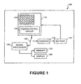
- FIG. 1 is a schematic representation of a mobile device 100 including an image sensor 110 in accordance with one embodiment of the invention.
- the mobile device 100 can be a cellular phone, a personal digital assistant (PDA), a video game console, a digital camera, a digital camcorder, a computing device, a wireless communication device, or another portable electronic device.
- the image sensor 110 is configured to selectively capture images of desired objects and provide current to recharge a battery in the mobile device 100.
- the illustrated mobile device 100 includes a signal processor 160, memory 170 electrically coupled to the signal processor 160, and a display 180 electrically coupled to the signal processor 160.
- the signal processor 160 is operably coupled to the image sensor 110 for processing signals generated by an array of pixels 120 on the image sensor 110. For example, when the image sensor 110 captures an image, the signal processor 160 can compress the signals (using image compression schemes such as JPEG, M-JPEG or MPEG) to reduce the data size and route the compressed signals to the memory 170. Moreover, the signal processor 160 can condition the signals from the image sensor 110 so that they are compatible with the display 180.
- the signal processor 160 can include one or more image encoders and decoders, memory, processor, microcontrollers, buffer, routers, timing circuitry, analog-to-digital converters, calibration circuitry, control circuitry, image processing circuitry (such as chromaticity), luminance signal processing circuitry, and/or other circuitry to process signals generated by the image sensor 110.
- the memory 170 can include volatile memory and/or non-volatile memory for storing signals from the signal processor 160.
- the display 180 can be attached, embedded, or otherwise native to the mobile device 100 to display signals from the signal processor 160.
- the display 180 can be one of a variety of display types suitable for mobile devices, such as liquid crystal display (LCD) or touchscreen.
- the display 180 can be a monochrome or color display.
- the mobile device 100 may also include a transceiver configured to transmit and receive wireless signals to and from another wireless device, and the signal processor 160 can compress and/or condition the signals for transmission to another device.
- the components of the mobile device 100 may be embodied as hardware, firmware, and/or software.
- the image sensor 110 and the signal processor 160 may comprise one chip, and the memory 170 may comprise yet another chip.
- the functionality of two or more chips may be embodied in a single chip such as a system-on-chip (SOC).
- SOC system-on-chip
- one or more components illustrated in Figure 1 may be omitted depending on the mobile device.
- more than one memory unit or a detachable or swappable memory unit may be included in the mobile device 100.
- the illustrated mobile device 100 further includes a battery 150 and a battery charger 152 both of which are contained within the housing of the device 100.
- the battery 150 powers the image sensor 110 and the other components of the device 100, and the battery charger 152 is operably coupled to the image sensor 110 to selectively charge the battery 150. More specifically, when the image sensor 110 is not capturing an image, the pixels 120 can provide signals or current to the battery charger 152 for charging the battery 150.
- the mobile device 100 includes a switch 140 movable between a first position (shown in Figure 1) and a second position (not shown).
- the switch 140 directs current from the image sensor 110 to the signal processor 160 so that the mobile device 100 can capture images.
- the switch 140 directs current from the image sensor 110 to the battery charger 152 for charging the battery 150.
- the switch 140 can be operably coupled to an actuatable switch (not shown) on the mobile device 100 that a user actuates to capture an image. In this case, the switch 140 moves from the second position to the first position when the user actuates the switch. After the image is captured, the switch 140 can move back to the second position.
- the image sensor 110 can be a single-chip color CMOS image sensor, such as those manufactured by Omnivision Technologies, Inc. of Sunnyvale, California, the assignee of the present invention.
- CMOS image sensors provide advantages over image sensors that use charge-coupled devices (CCDs), in that CCD image sensors have large sizes and power consumption that are not well suited for mobile devices.
- CCDs charge-coupled devices
- the image sensor can be a CCD.
- the illustrated image sensor 110 includes an array of pixels 120 and a timing/control circuit 130 operably coupled to the pixels 120.
- the timing/control circuit 130 operates the pixels 120 so that the pixels 120 produce signals either (a) in a sequence for the signal processor 160 to process, or (b) continuously and simultaneously for use in charging the battery 150.
- the timing/control circuit 130 can be operably coupled to the switch 140 and/or the actuatable switch discussed above so that the current from the pixels 120 is provided to the signal processor 160 or battery charger 152.
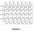
- Figure 2 is an enlarged schematic representation of the two-dimensional array of pixels 120 of Figure 1.
- the pixels 120 are arranged in columns 122 and rows 123, and although the illustrated embodiment includes seven columns 122 and four rows 123, other embodiments may include a different number of rows and columns.
- the individual pixels 120 are configured to convert incident light into an electrical signal, with the strength of the signal corresponding to the amount of light impinging on the pixel 120. These electrical signals can be used to charge the battery 150 ( Figure 1) or produce a digital image of the object reflecting light towards the pixels 120.
- the individual pixels 120 include a photodiode for generating an electrical signal and a transistor for controlling when the signal is output.
- Each pixel 120 in an individual column 122 outputs the electrical signal to a column signal line 124, which in turn transmits the signal to a column readout circuit 125.
- the column readout circuits 125 are shown at the "bottom" of Figure 2 for convenience purposes, the column readout circuits 125 can be placed almost anywhere on the integrated circuit relative to the array of pixels 120.
- the photodiodes when the image sensor 110 is used to capture an image of an object, the photodiodes generate electrical signals corresponding to the amount of light striking the pixels 120.
- the timing/control circuit 130 operates the pixels 120 so that the electrical signals of the pixels 120 are read out sequentially row-by-row. More specifically, one pixel 120 in each column 122 transmits its signal to the column readout circuit 125 at a single time. After the signals from one row 123 of pixels 120 are transmitted and read out at the column readout circuit 125, a subsequent row 123 of pixels 120 transmits signals to the column readout circuit 125. These signals are in turn transmitted from the column readout circuits 125 to the signal processor 160.
- the timing/control circuit 130 operates the pixels 120 so that the electrical signals from most, if not all, of the pixels 120 are transmitted simultaneously to the corresponding column readout circuits 125. Accordingly, more than one pixel 120 in each column 122 simultaneously transmits signals to the corresponding column readout circuit 125. Moreover, the pixels 120 continuously transmit signals to provide continuous current. The current from the pixels 120 is provided to the battery charger 152 to charge the battery 150.
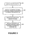
- FIG. 3 is a flow diagram illustrating the operation of the mobile device 100 in accordance with one method of an invention.
- the user actuates a switch to capture an image of an object.
- the switch 140 moves to the first position and the pixels 120 provide signals sequentially row-by-row to the column readout circuits 125 and, in turn, to the signal processor 160.
- the signal processor 160 provides image data to the display 180 and/or the memory 170.
- the switch 140 moves from the first position to the second position and the pixels 120 simultaneously provide continuous current to the charger 152 for charging the battery 150.
- the image sensor 110 is configured to capture images and provide current to charge the battery 150. As such, the image sensor 110 can provide current from the pixels 120 to the battery charger 152 when the image sensor 110 is not capturing an image.
- An advantage of this feature is that the frequency with which the mobile device 100 must be plugged into an AC power outlet to recharge the battery 150 is reduced.
Landscapes
- Engineering & Computer Science (AREA)
- Multimedia (AREA)
- Signal Processing (AREA)
- Power Engineering (AREA)
- Charge And Discharge Circuits For Batteries Or The Like (AREA)
- Transforming Light Signals Into Electric Signals (AREA)
- Secondary Cells (AREA)
- Studio Devices (AREA)
Abstract
Description
- The present invention relates to mobile devices with image sensors, and more particularly, to image sensors that selectively charge the battery in the mobile device.
- Integrated circuit technology has revolutionized various fields including computers, control systems, telecommunications, and imaging. In the imaging field, for example, CMOS image sensors have proved to be less expensive to manufacture than CCD imaging devices. Moreover, for certain applications, CMOS devices are superior in performance. Furthermore, the necessary signal processing logic on a CMOS image sensor can be integrated alongside the imaging circuitry, thus allowing for a single integrated chip to form a complete stand-alone imaging device. In other applications, however, CCD imaging devices still have some advantages.
- Image sensors are used to produce an image representing an object. The primary building block for an image formed by an image sensor is a pixel. Image sensors typically include a two-dimensional array of pixels arranged in rows and columns. The number, size, and spacing of the pixels determine the resolution of the image generated by the imaging device. The pixels of an image sensor are semiconductor devices that transform incident light photons into current signals. The photosignals are proportional to the amount of light reflected from an object to be imaged.
- In the array, pixels belonging to the same column (also referred to as bit line) are usually connected at a common output node. At the output node, a column readout circuit reads out and amplifies the photosignals from each pixel in the individual column. Typically, the pixels are read out row-by-row by asserting a row select signal to each pixel of the selected row. After the photosignals are read out, the signals are processed by signal processing circuitry to create an image representing the object.
- Personal digital assistants (PDAs), digital cameras, cell phones, and other portable electronic devices often include camera units with image sensors to capture images. These mobile devices include a battery to power the image sensor and other components of the device. Although CMOS imager sensors consume less power than CCD image sensors, both types of image sensors drain the battery. Power consumption is an issue in portable electronic devices because the charge in a typical battery lasts for a relatively short time. To recharge the battery, the device is generally coupled to an AC outlet or another power source. As such, the mobility of the device is reduced during charging. Accordingly, a need exists to reduce the frequency with which the battery of a mobile device must be recharged.
JP-A-2003008958 - The present invention provides a mobile device according to claim 1.
- The mobile devices can be cellular phones, personal digital assistants (PDAs), video game consoles, digital cameras, digital camcorders, computing devices, wireless communication devices, and/or other portable electronic devices. In one embodiment, the image sensor is configured to capture images as well as provide current to charge the battery. The mobile device may further include a housing, with the battery, battery charger, and image sensor contained within the housing.
- Another aspect of the invention is directed to methods for operating mobile devices as defined in claim 6. Charging the battery can occur before and/or after capturing the image. In one aspect of this embodiment, capturing the image includes powering the image sensor with the battery.
-
- Figure 1 is a schematic representation of a mobile device including an image sensor in accordance with one embodiment of the invention.
- Figure 2 is an enlarged schematic representation of a pixel array in the image sensor of Figure 1.
- Figure 3 is a flow diagram illustrating the operation of the mobile device of Figure 1 in accordance with one embodiment of the invention.
- Sizes of components are not drawn to scale, and various components may be enlarged or reduced to improve drawing legibility. Component details have been abstracted in the Figures to exclude details such as the position of components and the precise connections between such components when such details are unnecessary to the invention.
- In the following description, numerous specific details are provided, such as the identification of various components of mobile devices, to provide a thorough understanding of embodiments of the invention. One skilled in the art will recognize, however, that the invention can be practiced without one or more of the specific details, or with other methods, components, materials, etc. In still other instances, well-known structures, materials, or operations are not shown or described in detail to avoid obscuring aspects of various embodiments of the invention.
- Reference throughout this specification to "one embodiment" or "an embodiment" means that a particular feature, structure, or characteristic described in connection with the embodiment is included in at least one embodiment of the present invention. Thus, the appearance of the phrases "in one embodiment" or "in an embodiment" in various places throughout this specification are not necessarily all referring to the same embodiment. Furthermore, the particular features, structures, or characteristics may be combined in any suitable manner in one or more embodiments.
- Figure 1 is a schematic representation of a
mobile device 100 including animage sensor 110 in accordance with one embodiment of the invention. Themobile device 100 can be a cellular phone, a personal digital assistant (PDA), a video game console, a digital camera, a digital camcorder, a computing device, a wireless communication device, or another portable electronic device. As described in greater detail below, theimage sensor 110 is configured to selectively capture images of desired objects and provide current to recharge a battery in themobile device 100. - The illustrated
mobile device 100 includes asignal processor 160,memory 170 electrically coupled to thesignal processor 160, and adisplay 180 electrically coupled to thesignal processor 160. Thesignal processor 160 is operably coupled to theimage sensor 110 for processing signals generated by an array ofpixels 120 on theimage sensor 110. For example, when theimage sensor 110 captures an image, thesignal processor 160 can compress the signals (using image compression schemes such as JPEG, M-JPEG or MPEG) to reduce the data size and route the compressed signals to thememory 170. Moreover, thesignal processor 160 can condition the signals from theimage sensor 110 so that they are compatible with thedisplay 180. Accordingly, thesignal processor 160 can include one or more image encoders and decoders, memory, processor, microcontrollers, buffer, routers, timing circuitry, analog-to-digital converters, calibration circuitry, control circuitry, image processing circuitry (such as chromaticity), luminance signal processing circuitry, and/or other circuitry to process signals generated by theimage sensor 110. - The
memory 170 can include volatile memory and/or non-volatile memory for storing signals from thesignal processor 160. Thedisplay 180 can be attached, embedded, or otherwise native to themobile device 100 to display signals from thesignal processor 160. Thedisplay 180 can be one of a variety of display types suitable for mobile devices, such as liquid crystal display (LCD) or touchscreen. Moreover, thedisplay 180 can be a monochrome or color display. In other embodiments, themobile device 100 may also include a transceiver configured to transmit and receive wireless signals to and from another wireless device, and thesignal processor 160 can compress and/or condition the signals for transmission to another device. - The components of the
mobile device 100 may be embodied as hardware, firmware, and/or software. For example, theimage sensor 110 and thesignal processor 160 may comprise one chip, and thememory 170 may comprise yet another chip. Alternatively, the functionality of two or more chips may be embodied in a single chip such as a system-on-chip (SOC). It should also be understood that one or more components illustrated in Figure 1 may be omitted depending on the mobile device. Moreover, if themobile device 100 is used primarily for capturing images/video, then more than one memory unit or a detachable or swappable memory unit, may be included in themobile device 100. - The illustrated
mobile device 100 further includes abattery 150 and abattery charger 152 both of which are contained within the housing of thedevice 100. Thebattery 150 powers theimage sensor 110 and the other components of thedevice 100, and thebattery charger 152 is operably coupled to theimage sensor 110 to selectively charge thebattery 150. More specifically, when theimage sensor 110 is not capturing an image, thepixels 120 can provide signals or current to thebattery charger 152 for charging thebattery 150. - In one embodiment, the
mobile device 100 includes aswitch 140 movable between a first position (shown in Figure 1) and a second position (not shown). In the first position, theswitch 140 directs current from theimage sensor 110 to thesignal processor 160 so that themobile device 100 can capture images. In the second position, theswitch 140 directs current from theimage sensor 110 to thebattery charger 152 for charging thebattery 150. Theswitch 140 can be operably coupled to an actuatable switch (not shown) on themobile device 100 that a user actuates to capture an image. In this case, theswitch 140 moves from the second position to the first position when the user actuates the switch. After the image is captured, theswitch 140 can move back to the second position. - The
image sensor 110 can be a single-chip color CMOS image sensor, such as those manufactured by Omnivision Technologies, Inc. of Sunnyvale, California, the assignee of the present invention. Such CMOS image sensors provide advantages over image sensors that use charge-coupled devices (CCDs), in that CCD image sensors have large sizes and power consumption that are not well suited for mobile devices. In additional embodiments, however, the image sensor can be a CCD. - The illustrated
image sensor 110 includes an array ofpixels 120 and a timing/control circuit 130 operably coupled to thepixels 120. The timing/control circuit 130 operates thepixels 120 so that thepixels 120 produce signals either (a) in a sequence for thesignal processor 160 to process, or (b) continuously and simultaneously for use in charging thebattery 150. As such, the timing/control circuit 130 can be operably coupled to theswitch 140 and/or the actuatable switch discussed above so that the current from thepixels 120 is provided to thesignal processor 160 orbattery charger 152. - Figure 2 is an enlarged schematic representation of the two-dimensional array of
pixels 120 of Figure 1. Thepixels 120 are arranged incolumns 122 androws 123, and although the illustrated embodiment includes sevencolumns 122 and fourrows 123, other embodiments may include a different number of rows and columns. Theindividual pixels 120 are configured to convert incident light into an electrical signal, with the strength of the signal corresponding to the amount of light impinging on thepixel 120. These electrical signals can be used to charge the battery 150 (Figure 1) or produce a digital image of the object reflecting light towards thepixels 120. - In one embodiment, the
individual pixels 120 include a photodiode for generating an electrical signal and a transistor for controlling when the signal is output. Eachpixel 120 in anindividual column 122 outputs the electrical signal to acolumn signal line 124, which in turn transmits the signal to acolumn readout circuit 125. Although thecolumn readout circuits 125 are shown at the "bottom" of Figure 2 for convenience purposes, thecolumn readout circuits 125 can be placed almost anywhere on the integrated circuit relative to the array ofpixels 120. - Referring to both Figures 1 and 2, when the
image sensor 110 is used to capture an image of an object, the photodiodes generate electrical signals corresponding to the amount of light striking thepixels 120. The timing/control circuit 130 operates thepixels 120 so that the electrical signals of thepixels 120 are read out sequentially row-by-row. More specifically, onepixel 120 in eachcolumn 122 transmits its signal to thecolumn readout circuit 125 at a single time. After the signals from onerow 123 ofpixels 120 are transmitted and read out at thecolumn readout circuit 125, asubsequent row 123 ofpixels 120 transmits signals to thecolumn readout circuit 125. These signals are in turn transmitted from thecolumn readout circuits 125 to thesignal processor 160. - When the
image sensor 110 is used to charge thebattery 150, the timing/control circuit 130 operates thepixels 120 so that the electrical signals from most, if not all, of thepixels 120 are transmitted simultaneously to the correspondingcolumn readout circuits 125. Accordingly, more than onepixel 120 in eachcolumn 122 simultaneously transmits signals to the correspondingcolumn readout circuit 125. Moreover, thepixels 120 continuously transmit signals to provide continuous current. The current from thepixels 120 is provided to thebattery charger 152 to charge thebattery 150. - Figure 3 is a flow diagram illustrating the operation of the
mobile device 100 in accordance with one method of an invention. Referring to Figures 1-3, atblock 200, the user actuates a switch to capture an image of an object. Atblock 202, theswitch 140 moves to the first position and thepixels 120 provide signals sequentially row-by-row to thecolumn readout circuits 125 and, in turn, to thesignal processor 160. Atblock 204, thesignal processor 160 provides image data to thedisplay 180 and/or thememory 170. Atblock 206, theswitch 140 moves from the first position to the second position and thepixels 120 simultaneously provide continuous current to thecharger 152 for charging thebattery 150. - One feature of the
mobile device 100 illustrated in Figures 1 and 2 is that theimage sensor 110 is configured to capture images and provide current to charge thebattery 150. As such, theimage sensor 110 can provide current from thepixels 120 to thebattery charger 152 when theimage sensor 110 is not capturing an image. An advantage of this feature is that the frequency with which themobile device 100 must be plugged into an AC power outlet to recharge thebattery 150 is reduced. - Unless the context clearly requires otherwise, throughout the description and the claims, the words "comprise," "comprising" and the like are to be construed in an inclusive sense as opposed to an exclusive or exhaustive sense; that is to say, in a sense of "including, but not limited to." Words using the singular or plural number also include the plural or singular number, respectively. Additionally, the words "herein," "above," "below," and words of similar import, when used in this application, shall refer to this application as a whole and not to any particular portion of this application. When the claims use the words "or" in reference to a list of two or more items, that word covers all of the following interpretations of the word: any of the items in the list, all of the items in the list, and any combination of the items in the list.
- From the foregoing, it will be appreciated that specific embodiments of the invention have been described herein for purposes of illustration, but that various modifications may be made without deviating from the scope of the invention. Accordingly, the invention is not limited except as by the appended claims.
Claims (8)
- A mobile device, comprising:a battery (150);a battery charger (152) electrically coupled to the battery (150); anda signal processor (160);an image sensor (110) operably coupled to the battery charger to selectively charge the battery (150), wherein the image sensor (110) comprises an array of pixels (120); andcharacterised in that:the mobile device further comprises a switch (140) to(a) direct current from the pixels (120) to the signal processor (160) when the image sensor captures images, and(b) direct current from the pixels (120) to the battery charger (152) when the battery charger charges the battery;the image sensor comprises a timing/control circuit (130) for controlling the pixels to selectively provide constant current from the pixels to the battery charger and the array of pixels is arranged in columns (120), wherein the timing/control circuit selectively controls the pixels so that multiple pixels in an individual column provide current to the battery charger simultaneously;the image sensor comprises a color complimentary metal oxide semiconductor (CMOS) image sensor; andthe mobile device further comprises a user-actuatable switch for actuation by a user to capture an image, the user-actuatable switch being operably coupled to the switch (140) so that current is directed by the switch (140) from the pixels to the signal processor (160) when a user actuates the user-actuatable switch to capture an image and current is - directed by the switch (140) from the pixels to the battery charger (152) after the image is captured.
- The mobile device of claim 1 wherein:the image sensor is configured to capture images; andthe image sensor is configured to provide current for charging the battery before and/or after capturing images.
- The mobile device of claim 1 wherein:the image sensor is configured to capture images; andthe battery powers the image sensor when the image sensor captures images.
- The mobile device of claim 1, further comprising a housing, wherein the battery, battery charger, and image sensor are contained within the housing.
- The mobile device of claim 1, further comprising a camera unit including the image sensor.
- A method for operating a mobile device having an image sensor (110) comprising an array of pixels (120), a battery (150), a battery charger (152) and a signal processor (160), wherein:the mobile device further comprises a switch (140) to(a) direct current from the pixels (120) to the signal processor (160) when the image sensor captures images, and(b) direct current from the pixels (120) to the battery charger (152) when the battery charger charges the battery;the image sensor comprises a timing/control (130) for controlling the pixels and the array of pixels is arranged in columns;the image sensor comprises a color complimentary metal oxide semiconductor (CMOS) image sensor; andthe mobile device further comprises a user-actuatable switch for actuation by a user to capture an image, the user-actuatable switch being operably coupled to the switch (140) so that current is directed by the switch (140) from the pixels to the signal processor (160) when a user actuates the user-actuatable switch to capture an image and current is directed by the switch (140) from the pixels to the battery charger (152) after the image is captured;the method comprising:capturing an image with an image sensor by directing current from the pixels to the signal processor,characterised in that the method includes:charging the battery (150) with the image sensor by directing current from the pixels (120) to the battery charger (152), wherein charging the battery comprises providing constant current from the pixels to the battery charger and controlling the pixels with the timing/control circuit so that multiple pixels in an individual column provide current to the battery charger simultaneously; andactuation of the user-actuatable switch by a user to capture an image wherein current is directed by the switch (140) from the pixels to the signal processor when the user actuates the user-actuatable switch to capture the image and current is directed by the switch (140) from the pixels to the battery charger after the image is captured.
- The method of claim 6 wherein charging the battery occurs before and/or after capturing the image.
- The method of claim 6 wherein capturing the image comprises powering the image sensor with the battery.
Applications Claiming Priority (2)
| Application Number | Priority Date | Filing Date | Title |
|---|---|---|---|
| US10/808,655 US7405763B2 (en) | 2004-03-24 | 2004-03-24 | Mobile devices having an image sensor for charging a battery |
| US808655 | 2004-03-24 |
Publications (2)
| Publication Number | Publication Date |
|---|---|
| EP1580864A1 EP1580864A1 (en) | 2005-09-28 |
| EP1580864B1 true EP1580864B1 (en) | 2007-11-28 |
Family
ID=34862074
Family Applications (1)
| Application Number | Title | Priority Date | Filing Date |
|---|---|---|---|
| EP05251035A Expired - Lifetime EP1580864B1 (en) | 2004-03-24 | 2005-02-23 | Mobile devices having an image sensor for charging a battery |
Country Status (6)
| Country | Link |
|---|---|
| US (2) | US7405763B2 (en) |
| EP (1) | EP1580864B1 (en) |
| CN (1) | CN100394640C (en) |
| AT (1) | ATE379868T1 (en) |
| DE (1) | DE602005003497T2 (en) |
| TW (1) | TWI305698B (en) |
Families Citing this family (15)
| Publication number | Priority date | Publication date | Assignee | Title |
|---|---|---|---|---|
| US7405763B2 (en) * | 2004-03-24 | 2008-07-29 | Omnivision Technologies, Inc. | Mobile devices having an image sensor for charging a battery |
| DE102008034279B4 (en) * | 2008-07-22 | 2012-04-26 | Fraunhofer-Gesellschaft zur Förderung der angewandten Forschung e.V. | A method for energy self-sufficient operation of a device and a self-powered device with one or more photosensitive sensor elements |
| US8629386B2 (en) * | 2009-02-27 | 2014-01-14 | The Hong Kong University Of Science And Technology | Method and apparatus for energy harvesting using CMOS sensor |
| KR101070612B1 (en) * | 2009-09-29 | 2011-10-10 | 한국과학기술원 | Image sensor, method for operating the image sensor, and image pick-up device having the image sensor |
| CA2835870A1 (en) | 2011-05-12 | 2012-11-15 | Olive Medical Corporation | Pixel array area optimization using stacking scheme for hybrid image sensor with minimal vertical interconnects |
| US9105538B2 (en) * | 2011-06-14 | 2015-08-11 | Moon J. Kim | Dynamically configurable photovoltaic cell array |
| TWI568134B (en) * | 2011-10-24 | 2017-01-21 | 仁寶電腦工業股份有限公司 | Charging control method |
| MX344146B (en) | 2012-07-26 | 2016-12-07 | Depuy Synthes Products Inc | Camera system with minimal area monolithic cmos image sensor. |
| AU2014223163A1 (en) | 2013-02-28 | 2015-08-20 | Olive Medical Corporation | Videostroboscopy of vocal chords with CMOS sensors |
| US10750933B2 (en) | 2013-03-15 | 2020-08-25 | DePuy Synthes Products, Inc. | Minimize image sensor I/O and conductor counts in endoscope applications |
| CN105246394B (en) | 2013-03-15 | 2018-01-12 | 德普伊新特斯产品公司 | It is synchronous without the imaging sensor of input clock and data transfer clock |
| WO2016112204A1 (en) | 2015-01-07 | 2016-07-14 | Nayar Shree K | Circuits for self-powered image sensors |
| US9407845B1 (en) * | 2015-03-26 | 2016-08-02 | Amazon Technologies, Inc. | Self powering camera |
| US10403656B2 (en) * | 2016-07-14 | 2019-09-03 | Purdue Research Foundation | Energy harvesting configurable image sensor |
| WO2019165288A1 (en) | 2018-02-23 | 2019-08-29 | The Regents Of The University Of Michigan | Imaging sensor and pixel structure for simultaneous imaging and energy harvesting |
Family Cites Families (23)
| Publication number | Priority date | Publication date | Assignee | Title |
|---|---|---|---|---|
| JPH026330A (en) | 1988-03-07 | 1990-01-10 | Sanyo Electric Co Ltd | Production of superconducting material and superconducting single crystal |
| JPH0263330A (en) | 1988-08-30 | 1990-03-02 | Ricoh Co Ltd | Photoelectric converter |
| GB9524483D0 (en) * | 1995-11-30 | 1996-01-31 | Philips Electronics Nv | Light sensing array device and apparatus incorporating such |
| US6721008B2 (en) * | 1998-01-22 | 2004-04-13 | Eastman Kodak Company | Integrated CMOS active pixel digital camera |
| JP2000050132A (en) * | 1998-07-29 | 2000-02-18 | Fuji Photo Film Co Ltd | Electronic camera and method for controlling its operation |
| WO2000038415A1 (en) | 1998-12-22 | 2000-06-29 | California Institute Of Technology | Highly miniaturized, battery operated, digital wireless camera |
| US6778212B1 (en) * | 2000-02-22 | 2004-08-17 | Pixim, Inc. | Digital image sensor with on -chip programmable logic |
| JP2002094873A (en) * | 2000-09-14 | 2002-03-29 | Fuji Photo Film Co Ltd | Digital camera |
| US6803553B1 (en) * | 2001-05-23 | 2004-10-12 | Pixim, Inc. | Image sensor with charge recycling |
| CA2351025A1 (en) * | 2001-06-19 | 2002-12-19 | Symagery Microsystems Inc. | Method and apparatus for controlling power consumption in an active pixel sensor array |
| JP2003008958A (en) | 2001-06-21 | 2003-01-10 | Fuji Film Microdevices Co Ltd | Image pickup device |
| US6914227B2 (en) * | 2001-06-25 | 2005-07-05 | Canon Kabushiki Kaisha | Image sensing apparatus capable of outputting image by converting resolution by adding and reading out a plurality of pixels, its control method, and image sensing system |
| JP3539414B2 (en) * | 2001-09-25 | 2004-07-07 | 株式会社日立製作所 | Information recording device |
| US6734413B2 (en) * | 2001-11-06 | 2004-05-11 | Omnivision Technologies, Inc. | Zero DC current readout circuit for CMOS image sensor using a precharge capacitor |
| JP2003179820A (en) * | 2001-12-11 | 2003-06-27 | Hitachi Ltd | Imaging system and imaging apparatus using CMOS solid-state imaging device |
| US7068319B2 (en) * | 2002-02-01 | 2006-06-27 | Micron Technology, Inc. | CMOS image sensor with a low-power architecture |
| US6730900B2 (en) * | 2002-02-05 | 2004-05-04 | E-Phocus, Inc. | Camera with MOS or CMOS sensor array |
| JP2004112422A (en) * | 2002-09-19 | 2004-04-08 | Canon Inc | Imaging device |
| US7782377B2 (en) * | 2003-02-26 | 2010-08-24 | Canon Kabushiki Kaisha | Image sensing apparatus, control method therefor, storage medium, and program to create correction data |
| US20040257463A1 (en) * | 2003-06-17 | 2004-12-23 | Goris Andrew C. | User interface for digital camera having nonvolatile memory for storing intermediate data for advanced processing and capable of slowing, delaying and/or suspending advanced processing during low battery conditions |
| US7405763B2 (en) * | 2004-03-24 | 2008-07-29 | Omnivision Technologies, Inc. | Mobile devices having an image sensor for charging a battery |
| US7605398B2 (en) * | 2005-08-26 | 2009-10-20 | National Chung Cheng University | Apparatus of high dynamic-range CMOS image sensor and method thereof |
| US8629386B2 (en) * | 2009-02-27 | 2014-01-14 | The Hong Kong University Of Science And Technology | Method and apparatus for energy harvesting using CMOS sensor |
-
2004
- 2004-03-24 US US10/808,655 patent/US7405763B2/en not_active Expired - Lifetime
-
2005
- 2005-02-04 TW TW094103710A patent/TWI305698B/en not_active IP Right Cessation
- 2005-02-23 EP EP05251035A patent/EP1580864B1/en not_active Expired - Lifetime
- 2005-02-23 AT AT05251035T patent/ATE379868T1/en not_active IP Right Cessation
- 2005-02-23 DE DE602005003497T patent/DE602005003497T2/en not_active Expired - Fee Related
- 2005-03-23 CN CNB2005100601042A patent/CN100394640C/en not_active Expired - Lifetime
-
2008
- 2008-05-27 US US12/127,158 patent/US7936394B2/en not_active Expired - Lifetime
Also Published As
| Publication number | Publication date |
|---|---|
| ATE379868T1 (en) | 2007-12-15 |
| TWI305698B (en) | 2009-01-21 |
| DE602005003497T2 (en) | 2008-10-16 |
| EP1580864A1 (en) | 2005-09-28 |
| CN100394640C (en) | 2008-06-11 |
| US20050212957A1 (en) | 2005-09-29 |
| TW200601663A (en) | 2006-01-01 |
| US7405763B2 (en) | 2008-07-29 |
| CN1674349A (en) | 2005-09-28 |
| US20080225160A1 (en) | 2008-09-18 |
| DE602005003497D1 (en) | 2008-01-10 |
| US7936394B2 (en) | 2011-05-03 |
Similar Documents
| Publication | Publication Date | Title |
|---|---|---|
| US7936394B2 (en) | Mobile devices having an image sensor for charging a battery | |
| US7286170B2 (en) | Solid-state image sensor, camera using the same, camera control system, and signal output device | |
| CN101193216B (en) | Solid-state imaging device and imaging device | |
| CN106341628B (en) | Image sensor with wide dynamic range, pixel circuit and method of operation | |
| CN102124566B (en) | High-gain readout circuitry for 3D composite pixels | |
| CN108270981B (en) | Pixel unit, imaging method and imaging device thereof | |
| US10623673B2 (en) | Imaging device, imaging method, and imaging program | |
| US6946636B2 (en) | Image pickup apparatus providing a bias between different pixel areas during signal accumulation | |
| US20090237540A1 (en) | Imager method and apparatus having combined gate signals | |
| US20130214125A1 (en) | Method and apparatus for ambient light detection | |
| US20030160883A1 (en) | Single chip cmos image sensor system with video compression | |
| WO2022268216A1 (en) | Pixel structure, image sensor, control method and apparatus, and electronic device | |
| US12363446B2 (en) | Image sensor processing merged image and image processing system comprising the same | |
| US11637963B2 (en) | Image sensor and image processing system comprising the same | |
| US10075686B2 (en) | Color-image-data contamination correction device and imaging device, and method for controlling operation thereof | |
| US7019774B2 (en) | Imaging apparatus and mobile terminal incorporating same | |
| WO2018055948A1 (en) | Imaging device, operation method for imaging device, and operation program for imaging device | |
| CN111108743B (en) | Imaging control device, imaging device, imaging control method, and recording medium | |
| JP2021044623A (en) | Imaging apparatus and control method for the same | |
| US20050068435A1 (en) | Imaging device and imaging method | |
| US20170366771A1 (en) | Comparing circuit and an image sensor including a current stabilization circuit | |
| JP2008236634A (en) | Solid-state imaging device and imaging device | |
| KR20200122824A (en) | Light sensing circuit and image sensor comprising the same | |
| Kawahito et al. | A CMOS smart image sensor LSI for focal-plane compression | |
| US7060958B1 (en) | Compact-size image-sensing device and image-sensing element thereof |
Legal Events
| Date | Code | Title | Description |
|---|---|---|---|
| PUAI | Public reference made under article 153(3) epc to a published international application that has entered the european phase |
Free format text: ORIGINAL CODE: 0009012 |
|
| AK | Designated contracting states |
Kind code of ref document: A1 Designated state(s): AT BE BG CH CY CZ DE DK EE ES FI FR GB GR HU IE IS IT LI LT LU MC NL PL PT RO SE SI SK TR |
|
| AX | Request for extension of the european patent |
Extension state: AL BA HR LV MK YU |
|
| 17P | Request for examination filed |
Effective date: 20051014 |
|
| AKX | Designation fees paid |
Designated state(s): AT BE BG CH CY CZ DE DK EE ES FI FR GB GR HU IE IS IT LI LT LU MC NL PL PT RO SE SI SK TR |
|
| GRAP | Despatch of communication of intention to grant a patent |
Free format text: ORIGINAL CODE: EPIDOSNIGR1 |
|
| GRAS | Grant fee paid |
Free format text: ORIGINAL CODE: EPIDOSNIGR3 |
|
| GRAA | (expected) grant |
Free format text: ORIGINAL CODE: 0009210 |
|
| AK | Designated contracting states |
Kind code of ref document: B1 Designated state(s): AT BE BG CH CY CZ DE DK EE ES FI FR GB GR HU IE IS IT LI LT LU MC NL PL PT RO SE SI SK TR |
|
| REG | Reference to a national code |
Ref country code: GB Ref legal event code: FG4D |
|
| REG | Reference to a national code |
Ref country code: IE Ref legal event code: FG4D |
|
| REG | Reference to a national code |
Ref country code: CH Ref legal event code: EP |
|
| REF | Corresponds to: |
Ref document number: 602005003497 Country of ref document: DE Date of ref document: 20080110 Kind code of ref document: P |
|
| PG25 | Lapsed in a contracting state [announced via postgrant information from national office to epo] |
Ref country code: ES Free format text: LAPSE BECAUSE OF FAILURE TO SUBMIT A TRANSLATION OF THE DESCRIPTION OR TO PAY THE FEE WITHIN THE PRESCRIBED TIME-LIMIT Effective date: 20080311 Ref country code: CH Free format text: LAPSE BECAUSE OF FAILURE TO SUBMIT A TRANSLATION OF THE DESCRIPTION OR TO PAY THE FEE WITHIN THE PRESCRIBED TIME-LIMIT Effective date: 20071128 Ref country code: SE Free format text: LAPSE BECAUSE OF FAILURE TO SUBMIT A TRANSLATION OF THE DESCRIPTION OR TO PAY THE FEE WITHIN THE PRESCRIBED TIME-LIMIT Effective date: 20080228 Ref country code: NL Free format text: LAPSE BECAUSE OF FAILURE TO SUBMIT A TRANSLATION OF THE DESCRIPTION OR TO PAY THE FEE WITHIN THE PRESCRIBED TIME-LIMIT Effective date: 20071128 Ref country code: LI Free format text: LAPSE BECAUSE OF FAILURE TO SUBMIT A TRANSLATION OF THE DESCRIPTION OR TO PAY THE FEE WITHIN THE PRESCRIBED TIME-LIMIT Effective date: 20071128 |
|
| NLV1 | Nl: lapsed or annulled due to failure to fulfill the requirements of art. 29p and 29m of the patents act | ||
| PG25 | Lapsed in a contracting state [announced via postgrant information from national office to epo] |
Ref country code: PL Free format text: LAPSE BECAUSE OF FAILURE TO SUBMIT A TRANSLATION OF THE DESCRIPTION OR TO PAY THE FEE WITHIN THE PRESCRIBED TIME-LIMIT Effective date: 20071128 Ref country code: BG Free format text: LAPSE BECAUSE OF FAILURE TO SUBMIT A TRANSLATION OF THE DESCRIPTION OR TO PAY THE FEE WITHIN THE PRESCRIBED TIME-LIMIT Effective date: 20080228 Ref country code: LT Free format text: LAPSE BECAUSE OF FAILURE TO SUBMIT A TRANSLATION OF THE DESCRIPTION OR TO PAY THE FEE WITHIN THE PRESCRIBED TIME-LIMIT Effective date: 20071128 Ref country code: FI Free format text: LAPSE BECAUSE OF FAILURE TO SUBMIT A TRANSLATION OF THE DESCRIPTION OR TO PAY THE FEE WITHIN THE PRESCRIBED TIME-LIMIT Effective date: 20071128 Ref country code: SI Free format text: LAPSE BECAUSE OF FAILURE TO SUBMIT A TRANSLATION OF THE DESCRIPTION OR TO PAY THE FEE WITHIN THE PRESCRIBED TIME-LIMIT Effective date: 20071128 Ref country code: IS Free format text: LAPSE BECAUSE OF FAILURE TO SUBMIT A TRANSLATION OF THE DESCRIPTION OR TO PAY THE FEE WITHIN THE PRESCRIBED TIME-LIMIT Effective date: 20080328 |
|
| PGFP | Annual fee paid to national office [announced via postgrant information from national office to epo] |
Ref country code: DE Payment date: 20080313 Year of fee payment: 4 |
|
| REG | Reference to a national code |
Ref country code: CH Ref legal event code: PL |
|
| PG25 | Lapsed in a contracting state [announced via postgrant information from national office to epo] |
Ref country code: AT Free format text: LAPSE BECAUSE OF FAILURE TO SUBMIT A TRANSLATION OF THE DESCRIPTION OR TO PAY THE FEE WITHIN THE PRESCRIBED TIME-LIMIT Effective date: 20071128 |
|
| ET | Fr: translation filed | ||
| PG25 | Lapsed in a contracting state [announced via postgrant information from national office to epo] |
Ref country code: CZ Free format text: LAPSE BECAUSE OF FAILURE TO SUBMIT A TRANSLATION OF THE DESCRIPTION OR TO PAY THE FEE WITHIN THE PRESCRIBED TIME-LIMIT Effective date: 20071128 Ref country code: DK Free format text: LAPSE BECAUSE OF FAILURE TO SUBMIT A TRANSLATION OF THE DESCRIPTION OR TO PAY THE FEE WITHIN THE PRESCRIBED TIME-LIMIT Effective date: 20071128 |
|
| PG25 | Lapsed in a contracting state [announced via postgrant information from national office to epo] |
Ref country code: SK Free format text: LAPSE BECAUSE OF FAILURE TO SUBMIT A TRANSLATION OF THE DESCRIPTION OR TO PAY THE FEE WITHIN THE PRESCRIBED TIME-LIMIT Effective date: 20071128 Ref country code: BE Free format text: LAPSE BECAUSE OF FAILURE TO SUBMIT A TRANSLATION OF THE DESCRIPTION OR TO PAY THE FEE WITHIN THE PRESCRIBED TIME-LIMIT Effective date: 20071128 Ref country code: RO Free format text: LAPSE BECAUSE OF FAILURE TO SUBMIT A TRANSLATION OF THE DESCRIPTION OR TO PAY THE FEE WITHIN THE PRESCRIBED TIME-LIMIT Effective date: 20071128 |
|
| PG25 | Lapsed in a contracting state [announced via postgrant information from national office to epo] |
Ref country code: PT Free format text: LAPSE BECAUSE OF FAILURE TO SUBMIT A TRANSLATION OF THE DESCRIPTION OR TO PAY THE FEE WITHIN THE PRESCRIBED TIME-LIMIT Effective date: 20080428 |
|
| PLBE | No opposition filed within time limit |
Free format text: ORIGINAL CODE: 0009261 |
|
| STAA | Information on the status of an ep patent application or granted ep patent |
Free format text: STATUS: NO OPPOSITION FILED WITHIN TIME LIMIT |
|
| PG25 | Lapsed in a contracting state [announced via postgrant information from national office to epo] |
Ref country code: MC Free format text: LAPSE BECAUSE OF NON-PAYMENT OF DUE FEES Effective date: 20080228 |
|
| PGFP | Annual fee paid to national office [announced via postgrant information from national office to epo] |
Ref country code: IE Payment date: 20080520 Year of fee payment: 4 |
|
| 26N | No opposition filed |
Effective date: 20080829 |
|
| PGFP | Annual fee paid to national office [announced via postgrant information from national office to epo] |
Ref country code: FR Payment date: 20080327 Year of fee payment: 4 |
|
| PG25 | Lapsed in a contracting state [announced via postgrant information from national office to epo] |
Ref country code: GR Free format text: LAPSE BECAUSE OF FAILURE TO SUBMIT A TRANSLATION OF THE DESCRIPTION OR TO PAY THE FEE WITHIN THE PRESCRIBED TIME-LIMIT Effective date: 20080229 Ref country code: EE Free format text: LAPSE BECAUSE OF FAILURE TO SUBMIT A TRANSLATION OF THE DESCRIPTION OR TO PAY THE FEE WITHIN THE PRESCRIBED TIME-LIMIT Effective date: 20071128 |
|
| PG25 | Lapsed in a contracting state [announced via postgrant information from national office to epo] |
Ref country code: CY Free format text: LAPSE BECAUSE OF FAILURE TO SUBMIT A TRANSLATION OF THE DESCRIPTION OR TO PAY THE FEE WITHIN THE PRESCRIBED TIME-LIMIT Effective date: 20071128 |
|
| GBPC | Gb: european patent ceased through non-payment of renewal fee |
Effective date: 20090223 |
|
| REG | Reference to a national code |
Ref country code: FR Ref legal event code: ST Effective date: 20091030 |
|
| PG25 | Lapsed in a contracting state [announced via postgrant information from national office to epo] |
Ref country code: DE Free format text: LAPSE BECAUSE OF NON-PAYMENT OF DUE FEES Effective date: 20090901 Ref country code: IE Free format text: LAPSE BECAUSE OF NON-PAYMENT OF DUE FEES Effective date: 20090223 |
|
| PG25 | Lapsed in a contracting state [announced via postgrant information from national office to epo] |
Ref country code: GB Free format text: LAPSE BECAUSE OF NON-PAYMENT OF DUE FEES Effective date: 20090223 Ref country code: FR Free format text: LAPSE BECAUSE OF NON-PAYMENT OF DUE FEES Effective date: 20090302 |
|
| PG25 | Lapsed in a contracting state [announced via postgrant information from national office to epo] |
Ref country code: HU Free format text: LAPSE BECAUSE OF FAILURE TO SUBMIT A TRANSLATION OF THE DESCRIPTION OR TO PAY THE FEE WITHIN THE PRESCRIBED TIME-LIMIT Effective date: 20080529 Ref country code: LU Free format text: LAPSE BECAUSE OF NON-PAYMENT OF DUE FEES Effective date: 20080223 |
|
| PG25 | Lapsed in a contracting state [announced via postgrant information from national office to epo] |
Ref country code: TR Free format text: LAPSE BECAUSE OF FAILURE TO SUBMIT A TRANSLATION OF THE DESCRIPTION OR TO PAY THE FEE WITHIN THE PRESCRIBED TIME-LIMIT Effective date: 20071128 |
|
| PG25 | Lapsed in a contracting state [announced via postgrant information from national office to epo] |
Ref country code: IT Free format text: LAPSE BECAUSE OF NON-PAYMENT OF DUE FEES Effective date: 20080229 |