EP1580647A2 - Mechanism for providing measured power management transitions in a microprocessor - Google Patents
Mechanism for providing measured power management transitions in a microprocessor Download PDFInfo
- Publication number
- EP1580647A2 EP1580647A2 EP04255567A EP04255567A EP1580647A2 EP 1580647 A2 EP1580647 A2 EP 1580647A2 EP 04255567 A EP04255567 A EP 04255567A EP 04255567 A EP04255567 A EP 04255567A EP 1580647 A2 EP1580647 A2 EP 1580647A2
- Authority
- EP
- European Patent Office
- Prior art keywords
- logic
- computing device
- recited
- power
- clock
- Prior art date
- Legal status (The legal status is an assumption and is not a legal conclusion. Google has not performed a legal analysis and makes no representation as to the accuracy of the status listed.)
- Ceased
Links
Images

Classifications
-
- G—PHYSICS
- G06—COMPUTING OR CALCULATING; COUNTING
- G06F—ELECTRIC DIGITAL DATA PROCESSING
- G06F1/00—Details not covered by groups G06F3/00 - G06F13/00 and G06F21/00
- G06F1/26—Power supply means, e.g. regulation thereof
- G06F1/32—Means for saving power
- G06F1/3203—Power management, i.e. event-based initiation of a power-saving mode
- G06F1/3234—Power saving characterised by the action undertaken
- G06F1/3237—Power saving characterised by the action undertaken by disabling clock generation or distribution
-
- G—PHYSICS
- G06—COMPUTING OR CALCULATING; COUNTING
- G06F—ELECTRIC DIGITAL DATA PROCESSING
- G06F1/00—Details not covered by groups G06F3/00 - G06F13/00 and G06F21/00
- G06F1/26—Power supply means, e.g. regulation thereof
- G06F1/32—Means for saving power
- G06F1/3203—Power management, i.e. event-based initiation of a power-saving mode
-
- Y—GENERAL TAGGING OF NEW TECHNOLOGICAL DEVELOPMENTS; GENERAL TAGGING OF CROSS-SECTIONAL TECHNOLOGIES SPANNING OVER SEVERAL SECTIONS OF THE IPC; TECHNICAL SUBJECTS COVERED BY FORMER USPC CROSS-REFERENCE ART COLLECTIONS [XRACs] AND DIGESTS
- Y02—TECHNOLOGIES OR APPLICATIONS FOR MITIGATION OR ADAPTATION AGAINST CLIMATE CHANGE
- Y02D—CLIMATE CHANGE MITIGATION TECHNOLOGIES IN INFORMATION AND COMMUNICATION TECHNOLOGIES [ICT], I.E. INFORMATION AND COMMUNICATION TECHNOLOGIES AIMING AT THE REDUCTION OF THEIR OWN ENERGY USE
- Y02D10/00—Energy efficient computing, e.g. low power processors, power management or thermal management
Definitions
- This invention relates in general to the field of microelectronics, and more particularly to a mechanism for providing measured power management transitions in a computing device.
- Most present day computing devices provide some form of a low power state that is entered as a result of asserting an external signal, or executing a special-purpose instruction, or encountering a fatal error condition.
- stop grant and auto halt where the internal clock signals to most of the functional logic blocks on the microprocessor are stopped. Stopping the internal clock signals to these logic blocks significantly reduces the amount of power that is being consumed by the microprocessor. However, not all clock signals are stopped. Those which are provided to a small number of logic blocks (e.g., bus snoop logic, interrupt logic) must remain enabled to allow certain processor events to be handled, but for all intents and purposes, the microprocessor is essentially powered down.
- logic blocks e.g., bus snoop logic, interrupt logic
- the stop grant state is invoked by asserting the STPCLK# pin on the microprocessor.
- the auto halt state is invoked by executing a HALT instruction.
- an x86-compatible microprocessor is required to stop the clock signals to the appropriate logic elements on the chip.
- Other microprocessors enter their corresponding low power state via different mechanisms, but the manner by which they "power down" functional logic blocks is the same, that is, by stopping the clock signals that are provided to those functional logic blocks.
- a present day microprocessor will stop all of the clock signals that are routed to the logic elements that must be powered down. And the clock signals are all stopped during a single clock cycle. To exit from the low power state, the microprocessor will start all of the clock signal during a single clock cycle as well.
- surge compensation and voltage filtering components are indeed effective, yet the present inventors have observed that most of the components are required solely to handle the drastic reduction (or increase) in current that is incurred when a computing device enter (or exits) a low power state within a single clock cycle.
- the present inventors have also noted that entry into or exit from a low power state within a single clock cycle is entirely unnecessary from the standpoint of any application that is being executed on a computing device.
- the drastic change in current requirements of a particular computing device results in a significant compression of its own operating voltage as a consequence of on-die voltage drop due to parasitic loop inductance (i.e., package effect). For example, following packaging of a particular computing device, it is tested and "binned" according to its maximum operating frequency. Because the speed at which a transistor switches is based largely upon its supplied operating voltage, this significant drop in on-chip operating voltage forces designers to operate the computing device at a lower frequency in order to produce correct results.
- a method is desirable that would enable entry into or exit from a low power state that does not impose unnecessary surge compensation requirements on a power source.
- the present invention is directed to solving the above-noted problems and addresses other problems, disadvantages, and limitations of the prior art.
- the present invention provides a superior technique for enabling measured and graceful power management transitions in a computing device that allows for less stringent voltage surge compensation mechanisms to be employed in an associated power supply and within the computing device itself, resulting in systems that are less costly than have heretofore been provided.
- an apparatus for providing measured power transitions in a computing device is envisioned.
- the apparatus includes power control logic that is configured to determine if the computing device is to enter a low power state.
- the power control logic has a plurality of stop signals, each sequentially indicating that a corresponding clock signal be stopped.
- the corresponding clock signal is operatively coupled to a corresponding sector logic element within the computing device.
- the power transition management mechanism has interval logic and power control logic.
- the interval logic provides one or more programmable numbers of clock cycles.
- the power control logic is coupled to the interval logic.
- the power control logic receives the one or more programmable numbers, and employs the one or more programmable numbers to sequentially stop each of a plurality of clock signals that are coupled to each of a corresponding plurality of sector logic elements.
- Another aspect of the present invention comprehends a method for providing measured power transitions in a computing device.
- the method includes determining if the computing device is to enter a low power state, and sequentially stopping clock signals that are coupled to each of a plurality of sector logic elements.
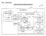
- FIGURE 1 is a block diagram illustrating how power is distributed in a present day computing device
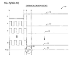
- FIGURE 2 is a timing diagram depicting how the computing device of FIGURE 1 enters a low power state
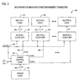
- FIGURE 3 is a block diagram featuring the mechanism for providing measured power management transitions according to the present invention.
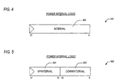
- FIGURE 4 is a block diagram showing one embodiment of power interval logic according to the present invention.
- FIGURE 5 is a block diagram illustrating another embodiment of power interval logic according to the present invention.
- FIGURE 6 is a timing diagram detailing how a computing device according to the present invention enters a low power state
- FIGURE 7 is a flow chart showing the method according to the present invention for providing measured power management transitions in a computing device.
- FIGURES 1 and 2 that more specifically describe the limitations of and problems associated with current techniques for taking a computing device to a low power state. Following this, a discussion of the present invention will be presented with reference to FIGURES 3-7.
- the present invention overcomes the limitations of present day power transition techniques by providing apparatus and methods for sequentially stopping the clocks provided to the functional logic elements within a computing device, thereby reducing the rate of current change that an associated power supply is currently required to support and consequently reducing the requirements to filter and/or suppress voltage transients.
- FIG. 1 a block diagram 100 is presented illustrating how power is distributed within a present day computing device 107.
- the block diagram 100 shows a power source 102 that provides power to the computing device 107 via a power bus PSVDD 104 and a return bus PSGND 105.
- the computing device 107 is coupled to the PSVDD bus 104 and the PSGND bus 105 via one or more pins (or leads) 108 on its package.
- the power bus 104 and return bus 105 are provided to some form of power distribution 109 that receives and filters the power, and that distributes the power to all logic devices 112, 115, 116 within the computing device 107 via a voltage bus VDD 110 and a ground bus 111.
- the power distribution 109 is no more than a distribution network of metal traces on a die.
- the computing device 107 also includes clock distribution logic 115 that distributes clock signals C1:CN 117 to a plurality of sector logic elements 116.
- Power state logic 112 is coupled to one or more external pins 108 and to a low power sense bus HALT 114. The power state logic 112 provides a low power signal LO 113 to the clock distribution logic 115.
- both the computing device 107 and the power source 102 are provided on a motherboard 101.
- the computing device 107 may be one of a number of different devices that distribute clock signals 117 to various sector logic elements 116 for the purpose of performing operations within the sector logic elements 116.
- the computing device 107 may be embodied as but not limited to any number of sequential logic devices, a graphics controller, logic within a chipset, a co-processor, a microcontroller, or a microprocessor.
- a graphics controller logic within a chipset
- a co-processor a co-processor
- a microcontroller or a microprocessor.
- the computing device 107 is embodied as a microprocessor 107 because the architecture of such is so widely known.
- the present inventors note however, that the scope and spirit of the present invention is not limited to embodiment of the computing device 107 solely as a microprocessor.
- Integrated computing devices 107 are configured as a plurality of sector logic elements 116.
- sector logic elements 116 are also referred to as functional units 116.
- a functional unit 116 is logic, circuits, devices, or microcode, or a combination of logic, circuits, devices, or microcode, or equivalent elements that are employed to perform an associated function within the microprocessor 107.
- the elements employed to perform the associated function may be shared with other circuits, microcode, etc., that are employed to perform other functions within the microprocessor 107.
- microcode is a term employed to refer to one or more micro instructions.
- a micro instruction (also referred to as a native instruction) is an instruction at the level that a functional unit 116 executes.
- micro instructions are directly executed by a reduced instruction set computer (RISC) microprocessor 107.
- RISC reduced instruction set computer
- CISC complex instruction set computer
- the sector 1 logic 116 could be an L1 data cache within the microprocessor 107.
- the sector 2 logic 116 could be an L2 cache within the microprocessor 107.
- Other sector logic elements 116 could be a branch prediction unit, a floating point execution unit, and integer execution unit, a register file, and so on.
- a present day computing device could conceivably comprise hundreds of sector logic elements 116.
- each of the sector logic elements 116 within the computing device 107 perform work as directed in synchronization with a provided clock signal 117. If the clock signal 117 is stopped, the work within a corresponding sector logic element 116 ceases. And since virtually all present day logic elements 116 are CMOS devices, one skilled in the art will appreciate that a given sector logic element 116 is drawing little or no current from the internal power buses 110, 111 when its corresponding clock signal 117 is stopped.
- the power source 102 is often embodied as a voltage regulator 102 mounted to the motherboard 101.
- the power source supplies a power voltage, such as 3.3 volts, over the power bus PSVDD 104 to power pins 108 on the microprocessor 107.
- the PSGNG bus 105 typically supplies a return voltage to which the GND bus 111 within the microprocessor 107 is referenced.
- the power distribution 109 filters the voltage supplied from the power source 102 and directly distributes this voltage to the sector logic elements 116. Alternatively, the power distribution 109 may translate the supplied voltage into a core voltage, such as a 1.5-volt core voltage, and then distribute the core voltage to the logic elements 116 over the VDD bus 110.
- any number of events, signals, or circumstances may transpire which would cause a computing device 107 that is operating in one power mode to transition to a low power mode and to exit from that low power mode to a different operating mode.
- the low power mode i.e., stop grant state
- STPCLK# an external signal that directs the computing device 107 to enter its low power state
- signal STOPCLK 106 which is received through a pin 108 and which is routed to the power state logic 112.
- signal HALT 114 which is provided to the power state logic 112.
- Signal HALT 114 is asserted when an instruction or event other than an external signal assertion directs the computing device 107 to enter its low power state. And whether directed by external signal STOPCLK 106 or by internal signal HALT 114, it is assumed for purposes of teaching the present invention that the low power state for the computing device 107 is entered by stopping the clock signals 117 to designated sector logic elements 116 and the low power state is exited by starting the clock signals 117 to designated sector logic elements 116.
- One skilled in the art will appreciate that a given computing device 107 may have more than one low power state where different combinations of sector logic elements 116 are powered down by stopping their respective clock signals 117. The present invention, as described below, comprehends such a configuration.
- the power state logic 112 when directed to enter the low power state, directs the clock distribution logic 115 to stop designated clock signals 117 to their corresponding sector logic elements 116 by asserting signal LO 113. In turn, the clock distribution logic 115 stops the designated clock signals 117 typically within a single clock cycle.
- This drastic reduction in current over the VDD and GND buses 110, 111 is translated to the PSVDD and PSGND buses 104, 105 such that a significant stress is placed upon the power source 102 to suppress voltage transients that would otherwise be seen on the external supply buses 104, 104 and internal power buses 110, 111.
- Present day power sources 102 consequently provide a power transient filter 103 to suppress voltage transients resulting from rapid current changes.
- a present day computing device 107 will provide numerous on-chip transient suppression devices (i.e., capacitive devices) (not shown) to suppress both low and high frequency voltage transients. Moreover, a present day computing device 107 will be limited in its upper operating frequency as a result of the on-chip voltage drop that is incurred from parasitic loop inductance when operating current rapidly changes. The effects of a rapid reduction in current within the computing device 107 through entering a low power state will now be discussed more specifically with reference to FIGURE 2.
- FIGURE 2 a timing diagram 200 is shown depicting how the computing device 107 of FIGURE 1 enters its low power state.
- the timing diagram 200 depicts signal LO 113 that is asserted at time T1, directing the clock distribution logic 115 to stop designated clock signals 117, thus causing the computing device 107 to enter the low power state.
- all of the clock signals C1:CN 117 are stopped for entry into the low power state.
- the clock distribution logic 115 stops clock signals C1:CN one clock cycle later at time T2. Because the current requirements of the computing device 107 significantly decrease at time T2, power generation elements (not shown) within the power source 102 are notably stressed.
- the external power bus PSVDD 104 is shown in the timing diagram 200 to remain approximately at a constant supply voltage when the clock signals 117 are stopped at time T2. This is because such a power state transition is well understood in the art and, consequently, transient suppression requirements are allocated to the power supply 102 to maintain an approximately constant voltage on bus PSVDD 104 in the event that such a transition occurs. Accordingly, the power supply 102 includes a filter 103 as described above that satisfies the allocated transient suppression requirements.
- Dashed transient 201 starting at time T2 and ending at time T3, is provided to depict a typical voltage transient 201 that would otherwise be transmitted on the external power supply bus 104, on the external power return bus PSGND 105 (i.e., a transient such as transient 201 superimposed at the reference voltage), and to a lesser degree on the internal VDD bus 110 and internal GND bus 111 as a result of parasitic loop inductances.
- the transient effect 201 of stopping the clocks C1:CN 117 concurrently at time T2 is not transmitted through to the computing device 107 at a level which would degrade performance.
- Expensive transient suppression filters 103 are added to the design of present day power sources 102 to provide for rapid decreases - and increases (i.e., when a low power state is exited) - in current provided to a coupled computing device 107.
- these rapid increases (and decreases) in current are due in large part to the manner in which a present day computing device enters into (and exits from) a low power state.
- the present inventors have also observed that it is entirely unnecessary to simultaneously "power down" all of the sector logic elements 116 that are not required to be operational in a low power state.
- the mechanism 300 includes power control logic 305 that is coupled to power interval logic 306 via an interval bus INT 308.
- the power control logic 305 provides a plurality of stop signals STOP1:STOPN to a corresponding plurality of clock distribution logic elements 302.
- Each of the clock distribution logic elements 302 receives a clock signal ECLOCK 304 and provide a local clock signal C1:CN 303 to their associated sector logic elements 301.
- the ECLOCK signal 304 is also provided to the power control logic 305.
- a low power state signal LO 307 is coupled to the power control logic 305.
- each of the sector logic elements 301 perform work as directed within a computing device (not shown) in synchronization with their individual local clock signals 303, which are synchronized with the ECLOCK clock signal 304. And like the sector logic elements 116 of FIGURE 1, if a particular clock signal 303 (say, signal C2 303) is stopped, then the work within its corresponding sector logic element 301 (i.e., SECTOR 2 LOGIC) ceases.
- FIGURE 3 For clarity purposes, power source and filtering elements are not shown in FIGURE 3 which provide voltage VDD and return GND to each of the logic elements in the mechanism 300. Nor is logic shown that senses assertion of signals, execution of instructions, or other events that would cause an associated computing device to enter its low power state. In accordance with the above discussion, it is assumed that signal LO 307 is asserted when a low power state is to be entered, and LO 307 is terminated when the low power state is to be exited.
- a single signal LO 307 is depicted in the block diagram, it is noted that the present invention contemplates a bus LO 307 whose state directs the power control logic 305 to enter into one of a plurality of low power states, where each of the plurality of low power states is entered by stopping the clock signals 303 to a corresponding combination of sector logic elements 301.
- the mechanism 300 when directed to enter the low power state, does not stop all designated clock signals 303 simultaneously. Instead, the power interval logic 306 provides a programmable number of clock cycles to the power control logic 305 via bus INT 308.
- the programmable number of clock cycles comprise a plurality of programmable numbers of clock cycles that correspond to each of the sector logic elements 301 that prescribe the number of clock cycles that are to transpire between stopping a given clock signal 303 (say, signal C2 303) to a given sector logic element 301 (i.e., SECTOR 2 LOGIC 301) and stopping a next clock signal 303 (say, signal C3 303) to a next sector logic element 301 (i.e., SECTOR 3 LOGIC 301).
- the programmable number of clock cycles comprises a single value that prescribes the number of clock cycles that are to transpire between stopping any clock signal 303 to its given sector logic element 301 and stopping a next clock signal 303 to a next sector logic element 301.
- the number of clock cycles that are provided via INT 308 are programmable for each of the sector logic elements 301.
- the number of clock cycles is a single number that applies to all of the sector logic elements.
- the power control logic Responsive to receipt of the programmable number of clock cycles via bus INT 308, the power control logic sequentially asserts the plurality of stop signals STOP1:STOPN 309 to their corresponding clock distribution logic 302 in synchronization with ECLOCK 304, but only after the number of clock cycles provided via bus INT 308 have transpired. Assertion of a STOP signal 309 directs the corresponding clock distribution logic element 302 to stop its clock signal 303 to its associated sector logic element 301. It is noted that the order in which the stop signals 309 are asserted is a function of the design of the power control logic 305, as is the combination of stop signals 309 which are asserted to enter a particular low power state.
- the power control logic 305 comprises logic, circuits, devices, or microcode, or a combination of logic, circuits, devices, or microcode, or equivalent elements that are employed to perform the aforementioned function within a computing device according to the present invention.
- the elements employed to perform the aforementioned function may be shared with other circuits, microcode, etc., that are employed to perform other functions within the computing device.
- the mechanism 300 As each of the stop signals 309 is asserted, its corresponding sector logic element 301 is "powered down.” And in contrast to the clock distribution logic 115 of FIGURE 1 which stops the clock signals 117 typically within a single clock cycle, the mechanism 300 according to the present invention provides for a graceful transition from one power state to the low power state. Hence, there is no drastic reduction in current requirements and, consequently, less stringent filtering requirements need be allocated to filtering devices (not shown) within an associated computing device or to its coupled power source (not shown).
- the power interval logic 400 comprises a register 400 that has a 32-bit INTERVAL field 401.
- the value of the INTERVAL field 401 is programmed to indicate a single number of clock cycles that are to transpire between stopping a given clock signal 303 to its given sector logic element 301 and stopping a next clock signal 303 to its next sector logic element 301.
- the value of the INTERVAL field 401 is programmed to indicate a single number of clock cycles that are to transpire between stopping a given clock signal 303 to its given sector logic element 301 and stopping a next clock signal 303 to its next sector logic element 301 and also to indicate (in the case of leaving a low power state) a single number of clock cycles that are to transpire between starting a given clock signal 303 to its given sector logic element 301 and starting a next clock signal 303 to its next sector logic element 301.
- the power interval logic 400 comprises logic, circuits, devices, or microcode, or a combination of logic, circuits, devices, or microcode, or equivalent elements that are employed to perform the aforementioned functions within a computing device according to the present invention.
- the elements employed to perform the aforementioned functions may be shared with other circuits, microcode, etc., that are employed to perform other functions within the computing device.
- the value of the INTERVAL field 401 is programmed by executing an instruction within the computing device that directs the computing device to set the value of the INTERVAL field 401.
- the value of the interval field is programmed according to the states of a plurality of fuses (not shown) that are operatively coupled to the power interval logic 400.
- the present invention also contemplates other techniques for setting the value of the INTERVAL field 401 to include reading a value from memory, setting the state of pins on a computing device package, and etc.
- a plurality of power interval logic elements 400 are provided that correspond in number to the number of sector logic elements 301 within the computing device.
- the power interval logic 500 comprises a register 400 that has a 16-bit UPINTERVAL field 401 and a 16-bit DOWNINTERVAL field 502.
- the value of the UPINTERVAL field 401 is programmed to indicate a single number of clock cycles that are to transpire (in the case of exiting a low power state) between starting a given clock signal 303 to its given sector logic element 301 and starting a next clock signal 303 to its next sector logic element 301.
- the value of the DOWNINTERVAL field 402 is programmed to indicate a single number of clock cycles that are to transpire (in the case of entering a low power state) between stopping a given clock signal 303 to its given sector logic element 301 and stopping a next clock signal 303 to its next sector logic element 301.
- the values of the fields 501, 502 are programmed in the same manner as the INTERVAL field 401 is programmed as discussed above with reference to the embodiment of FIGURE 4. Additionally, in an embodiment having separately programmable numbers of clock cycles for each sector logic element within a computing device according to the present invention, a plurality of power interval logic elements 500 are provided that correspond in number to the number of sector logic elements 301 within the computing device.
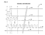
- FIGURE 6 a timing diagram 600 is shown detailing how a computing device according to the present invention enters a low power state.
- the timing diagram 400 depicts signal LO 307 that is asserted at time T1, directing the power control logic 305 to stop designated clock signals 303, thus causing the computing device to enter the low power state.
- all of the clock signals C1:CN 303 are stopped for entry into the low power state.
- the power control logic 305 Responsive to assertion of signal LO 307 at time T1, the power control logic 305 receives the value(s) of the power down interval(s) from the power interval logic 306 via bus 306 which indicates the number of clock cycles that are to transpire between stopping the clock signals 303 to sequential ones of the plurality of sector logic elements 301.
- the value of the power down interval is programmed to be two clock cycles and is a single value for all sector logic elements 302. Accordingly, the power control logic 305 asserts STOP1 signal 309 to the sector 1 clock distribution logic 302 causing clock signal C1 303 to stop at time T2, thus powering down SECTOR 1 LOGIC 301. Two clock cycles later, the power control logic 305 asserts STOP2 signal 309 to the sector 2 clock distribution logic 302 causing clock signal C2 303 to stop at time T3, thus powering down SECTOR 2 LOGIC 301. This sequence of successively turning off clock signals 303 continues every two clock cycles until finally the last clock signal CN 303 is turned off at time T4.
- An exemplary external power bus PSVDD 601 is shown in the timing diagram 400 to remain approximately at a constant supply voltage when the clock signals 303 are stopped in a measured manner between times T2 and T4 because transitioning power states in this manner does not put undue stress on a power source.
- FIGURE 7 a flow chart 700 is presented showing the method according to the present invention for providing measured power management transitions in a computing device.
- Flow begins at block 701 where the computing device is operating in a power state other than a low power state. Flow then proceeds to decision block 702.
- an evaluation is made to determine if the computing device should be taken to a low power state. If not, then flow proceeds to block 709. If a low power state is directed, then flow proceeds to block 703.
- a value INT is read from power interval logic according to the present invention.
- the value INT indicates the number of clock cycles that are to transpire between stopping a first clock signal to a first sector logic element and stopping a second clock signal to a second sector logic element. Flow then proceeds to block 704.
- a counter K is initialized to 1. Flow then proceeds to block 705.
- the counter K is evaluated to determine if all of the designated clock signals have been stopped. That is, for N clock signals, if K equals N+1, then all N clock signals have been stopped. If not, then flow proceeds to block 705. If so, then flow proceeds to block 709.
- a computing device By entering and leaving low power states in a measured manner as described hereinabove, a computing device according to the present invention provides for a controlled power transient characteristic that enables power supply and power regulation requirements to be significantly relaxed, thus decreasing the cost of the computing device itself, its associated power supply, and the overall system cost.
Landscapes
- Engineering & Computer Science (AREA)
- Theoretical Computer Science (AREA)
- Physics & Mathematics (AREA)
- General Engineering & Computer Science (AREA)
- General Physics & Mathematics (AREA)
- Power Sources (AREA)
- Control Of Voltage And Current In General (AREA)
Abstract
Description
Claims (16)
- An apparatus for providing measured power transitions in a computing device, the apparatus comprising:power control logic, configured to determine if the computing device is to enter a low power state, said power control logic comprising:a plurality of stop signals, each of said plurality of stop signals sequentially indicating that a corresponding clock signal be stopped, wherein said corresponding clock signal is operatively coupled to a corresponding sector logic element within the computing device.
- The apparatus as recited in claim 1, wherein said each of said plurality of stop signals indicates that said corresponding clock signal be stopped after a programmable number of clock cycles.
- The apparatus as recited in claim 2, wherein said programmable number of clock cycles is established for said each of said plurality of stop signals.
- The apparatus as recited in claim 2, wherein said programmable number of clock cycles is the same number of clock cycles for said each of said plurality of stop signals.
- The apparatus as recited in claim 1, further comprising:interval logic, coupled to said power control logic, configured to provide a programmable number of clock cycles to said power control logic, whereby said power control logic causes said each of said plurality of stop signals to indicate that said corresponding clock signal be stopped after said programmable number of clock cycles.
- The apparatus as recited in claim 5, wherein said interval logic comprises a register.
- The apparatus as recited in claim 6, wherein said programmable number is provided by executing an instruction to program said register.
- The apparatus as recited in claim 6, wherein said programmable number is provided by setting the state of fuses, said fuses being coupled to said register.
- An method for providing measured power transitions in a computing device, the method comprising:determining if the computing device is to enter a low power state; andsequentially stopping clock signals that are coupled to each of a plurality of sector logic elements.
- The method as recited in claim 9, wherein said sequentially stopping comprises:via each of a plurality of stop signals coupled to each of the plurality of sector logic elements, indicating that a corresponding one of the clock signals be stopped after a programmable number of clock cycles have transpired.
- The method as recited in claim 10, wherein said indicating comprises:establishing the programmable number of clock cycles for the each of the plurality of stop signals.
- The method as recited in claim 10, wherein said indicating comprises:establishing the same programmable number of clock cycles for the each of the plurality of stop signals.
- The method as recited in claim 10, further comprising:providing a programmable number of clock cycles that are to transpire between said stopping of the clock signals.
- The method as recited in claim 13, wherein said providing comprises:programming the programmable number of clock cycles into a register.
- The method as recited in claim 14, wherein said providing comprises:executing an instruction to accomplish said programming.
- The method as recited in claim 13, wherein said providing comprises:reading the states of fuses to accomplish said programming.
Applications Claiming Priority (2)
| Application Number | Priority Date | Filing Date | Title |
|---|---|---|---|
| US806041 | 1991-12-12 | ||
| US10/806,041 US7278040B2 (en) | 2003-03-21 | 2004-03-22 | Mechanism for providing measured power management transitions in a microprocessor |
Publications (2)
| Publication Number | Publication Date |
|---|---|
| EP1580647A2 true EP1580647A2 (en) | 2005-09-28 |
| EP1580647A3 EP1580647A3 (en) | 2007-04-18 |
Family
ID=34862030
Family Applications (1)
| Application Number | Title | Priority Date | Filing Date |
|---|---|---|---|
| EP04255567A Ceased EP1580647A3 (en) | 2004-03-22 | 2004-09-14 | Mechanism for providing measured power management transitions in a microprocessor |
Country Status (4)
| Country | Link |
|---|---|
| US (1) | US7278040B2 (en) |
| EP (1) | EP1580647A3 (en) |
| CN (1) | CN100410844C (en) |
| TW (1) | TWI250397B (en) |
Families Citing this family (11)
| Publication number | Priority date | Publication date | Assignee | Title |
|---|---|---|---|---|
| US7017059B2 (en) * | 2003-12-12 | 2006-03-21 | Cray Canada Inc. | Methods and apparatus for replacing cooling systems in operating computers |
| JP2006065471A (en) * | 2004-08-25 | 2006-03-09 | Fuji Xerox Co Ltd | Semiconductor integrated circuit, and its power saving control method and power saving control program |
| KR100852188B1 (en) | 2007-02-27 | 2008-08-13 | 삼성전자주식회사 | Dynamic Voltage Scaling System and Method |
| US8078891B2 (en) * | 2008-06-30 | 2011-12-13 | Intel Corporation | Method, device, and system for guaranteed minimum processor power state dwell time |
| US8990604B2 (en) | 2011-10-14 | 2015-03-24 | Apple Inc. | Alternately sensing voltage on supply side or load side of a power gate of an electronic device and modifying feedback input of a power supply controlled by the power gate based on which side of the power gate is currently sensed |
| US9444328B2 (en) * | 2012-06-26 | 2016-09-13 | Intel Corporation | Acoustic noise mitigation using periodicity disruption |
| CN106605201B (en) * | 2014-08-06 | 2021-11-23 | 苹果公司 | Reduced size user interface for battery management |
| AU2015312369B2 (en) | 2014-09-02 | 2018-04-05 | Apple Inc. | Reduced-size interfaces for managing alerts |
| US10951043B2 (en) | 2017-06-04 | 2021-03-16 | Apple Inc. | Multi-device charging user interface |
| US11646591B2 (en) | 2019-05-09 | 2023-05-09 | Apple Inc. | Indication for protective charging mode |
| US12530048B2 (en) * | 2022-04-25 | 2026-01-20 | Arm Limited | Methods and apparatus for controlling clock circuitry |
Family Cites Families (8)
| Publication number | Priority date | Publication date | Assignee | Title |
|---|---|---|---|---|
| US4835728A (en) * | 1986-08-13 | 1989-05-30 | Amdahl Corporation | Deterministic clock control apparatus for a data processing system |
| JP3742839B2 (en) * | 1992-07-21 | 2006-02-08 | レジェリティ・インコーポレイテッド | Clock generator that can be put into shutdown mode |
| JPH08202468A (en) * | 1995-01-27 | 1996-08-09 | Hitachi Ltd | Multiprocessor system |
| US5721935A (en) | 1995-12-20 | 1998-02-24 | Compaq Computer Corporation | Apparatus and method for entering low power mode in a computer system |
| US6115763A (en) * | 1998-03-05 | 2000-09-05 | International Business Machines Corporation | Multi-core chip providing external core access with regular operation function interface and predetermined service operation services interface comprising core interface units and masters interface unit |
| US6212645B1 (en) | 1998-10-09 | 2001-04-03 | Mediaq Inc. | Programmable and flexible power management unit |
| US6564328B1 (en) * | 1999-12-23 | 2003-05-13 | Intel Corporation | Microprocessor with digital power throttle |
| US7197654B2 (en) | 2002-04-11 | 2007-03-27 | International Business Machines Corporation | Method and apparatus for managing low power processor states |
-
2004
- 2004-03-22 US US10/806,041 patent/US7278040B2/en not_active Expired - Lifetime
- 2004-08-20 TW TW093125298A patent/TWI250397B/en not_active IP Right Cessation
- 2004-09-14 EP EP04255567A patent/EP1580647A3/en not_active Ceased
- 2004-12-31 CN CNB2004101031802A patent/CN100410844C/en not_active Expired - Lifetime
Also Published As
| Publication number | Publication date |
|---|---|
| EP1580647A3 (en) | 2007-04-18 |
| CN1629776A (en) | 2005-06-22 |
| CN100410844C (en) | 2008-08-13 |
| TW200532427A (en) | 2005-10-01 |
| TWI250397B (en) | 2006-03-01 |
| US7278040B2 (en) | 2007-10-02 |
| US20040236975A1 (en) | 2004-11-25 |
Similar Documents
| Publication | Publication Date | Title |
|---|---|---|
| US5560002A (en) | Method of testing a microprocessor by masking of an internal clock signal | |
| KR100399662B1 (en) | Configurable power management system with clock stabilization filter enabled or bypassed depending on the use of crystal or can oscillators | |
| US8850236B2 (en) | Power gating of cores by an SoC | |
| US7278040B2 (en) | Mechanism for providing measured power management transitions in a microprocessor | |
| US9503058B1 (en) | Relaxation oscillator | |
| KR100385155B1 (en) | Integrated processor with devices for multiplexing external pin signals | |
| EP2609481A1 (en) | Dynamic performance control of processing nodes | |
| US7398406B2 (en) | Data processor | |
| EP3593225A1 (en) | An operating point controller for circuit regions in an integrated circuit | |
| WO2009035950A1 (en) | Area and power saving standard cell methodology | |
| US5903747A (en) | Microprocessor clocking control system | |
| JP2001202155A (en) | Low power consumption processor | |
| KR20230021154A (en) | Programmable voltage regulation for data processor | |
| KR102786416B1 (en) | Power management based on limiting hardware-enforced power control | |
| US7408420B2 (en) | Multi mode clock generator | |
| Lee et al. | Web-based energy exploration tool for embedded systems | |
| US20250004536A1 (en) | Device, system, and method for providing isolation between cores to facilitate a multi-tenant environment | |
| US20040260960A1 (en) | Method for pulse train reduction of clocking power when switching between full clocking power and nap mode | |
| Processor | Preliminary | |
| US7847610B2 (en) | Semiconductor device, information processing apparatus and power supply voltage variation suppressing method | |
| US20250216878A1 (en) | Deep sleep power state with disabled inverse temperature dependency voltage regulation | |
| Six et al. | 8-bit AVR Microcontroller with 32K Bytes In-System Programmable Flash | |
| US20190377579A1 (en) | Microprocessor, power supply control ic, and power supply | |
| Set et al. | Independant CPU Frequency from USB Frequency–Watchdog Timer, Real-Time Clock Timer• Universal Serial Bus (USB)–Device 2.0 and Embedded Host Low Speed and Full Speed–Flexible End-Point Configuration and Management with Dedicated DMA Channels | |
| Jiménez et al. | Fundamentals of Interfacing |
Legal Events
| Date | Code | Title | Description |
|---|---|---|---|
| PUAI | Public reference made under article 153(3) epc to a published international application that has entered the european phase |
Free format text: ORIGINAL CODE: 0009012 |
|
| AK | Designated contracting states |
Kind code of ref document: A2 Designated state(s): AT BE BG CH CY CZ DE DK EE ES FI FR GB GR HU IE IT LI LU MC NL PL PT RO SE SI SK TR |
|
| AX | Request for extension of the european patent |
Extension state: AL HR LT LV MK |
|
| PUAL | Search report despatched |
Free format text: ORIGINAL CODE: 0009013 |
|
| AK | Designated contracting states |
Kind code of ref document: A3 Designated state(s): AT BE BG CH CY CZ DE DK EE ES FI FR GB GR HU IE IT LI LU MC NL PL PT RO SE SI SK TR |
|
| AX | Request for extension of the european patent |
Extension state: AL HR LT LV MK |
|
| 17P | Request for examination filed |
Effective date: 20070521 |
|
| 17Q | First examination report despatched |
Effective date: 20070717 |
|
| AKX | Designation fees paid |
Designated state(s): DE GB |
|
| STAA | Information on the status of an ep patent application or granted ep patent |
Free format text: STATUS: THE APPLICATION HAS BEEN REFUSED |
|
| 18R | Application refused |
Effective date: 20090923 |