EP1578582B1 - Electroformed adhesive laminated tooling surface with precision structured interfaces - Google Patents
Electroformed adhesive laminated tooling surface with precision structured interfaces Download PDFInfo
- Publication number
- EP1578582B1 EP1578582B1 EP03781916A EP03781916A EP1578582B1 EP 1578582 B1 EP1578582 B1 EP 1578582B1 EP 03781916 A EP03781916 A EP 03781916A EP 03781916 A EP03781916 A EP 03781916A EP 1578582 B1 EP1578582 B1 EP 1578582B1
- Authority
- EP
- European Patent Office
- Prior art keywords
- projections
- insert
- backing
- backing surface
- adhesive
- Prior art date
- Legal status (The legal status is an assumption and is not a legal conclusion. Google has not performed a legal analysis and makes no representation as to the accuracy of the status listed.)
- Expired - Lifetime
Links
- 239000000853 adhesive Substances 0.000 title claims abstract description 31
- 230000001070 adhesive effect Effects 0.000 title claims abstract description 31
- 238000000034 method Methods 0.000 claims abstract description 31
- 238000002347 injection Methods 0.000 claims abstract description 14
- 239000007924 injection Substances 0.000 claims abstract description 14
- PXHVJJICTQNCMI-UHFFFAOYSA-N Nickel Chemical compound [Ni] PXHVJJICTQNCMI-UHFFFAOYSA-N 0.000 claims description 16
- RYGMFSIKBFXOCR-UHFFFAOYSA-N Copper Chemical compound [Cu] RYGMFSIKBFXOCR-UHFFFAOYSA-N 0.000 claims description 13
- 239000010949 copper Substances 0.000 claims description 13
- 229910052802 copper Inorganic materials 0.000 claims description 12
- 229910052751 metal Inorganic materials 0.000 claims description 10
- 239000002184 metal Substances 0.000 claims description 10
- 229910000881 Cu alloy Inorganic materials 0.000 claims description 8
- 229910052759 nickel Inorganic materials 0.000 claims description 8
- 239000000463 material Substances 0.000 claims description 7
- 229920000647 polyepoxide Polymers 0.000 claims description 7
- 229910000831 Steel Inorganic materials 0.000 claims description 6
- 239000010959 steel Substances 0.000 claims description 6
- 239000003822 epoxy resin Substances 0.000 claims description 5
- 229910052782 aluminium Inorganic materials 0.000 claims description 3
- XAGFODPZIPBFFR-UHFFFAOYSA-N aluminium Chemical compound [Al] XAGFODPZIPBFFR-UHFFFAOYSA-N 0.000 claims description 3
- 238000010276 construction Methods 0.000 claims description 3
- 229920006332 epoxy adhesive Polymers 0.000 claims description 3
- 239000013464 silicone adhesive Substances 0.000 claims description 3
- 239000002131 composite material Substances 0.000 claims description 2
- 238000005323 electroforming Methods 0.000 claims description 2
- 238000007747 plating Methods 0.000 claims description 2
- XEEYBQQBJWHFJM-UHFFFAOYSA-N Iron Chemical compound [Fe] XEEYBQQBJWHFJM-UHFFFAOYSA-N 0.000 claims 4
- 229910000990 Ni alloy Inorganic materials 0.000 claims 2
- 229910052742 iron Inorganic materials 0.000 claims 2
- 239000000126 substance Substances 0.000 claims 1
- 229920001169 thermoplastic Polymers 0.000 abstract description 3
- 239000004416 thermosoftening plastic Substances 0.000 abstract description 3
- 239000010410 layer Substances 0.000 description 6
- 238000004519 manufacturing process Methods 0.000 description 5
- 229920000642 polymer Polymers 0.000 description 5
- 239000004593 Epoxy Substances 0.000 description 4
- 238000001746 injection moulding Methods 0.000 description 4
- 238000000465 moulding Methods 0.000 description 4
- 238000012546 transfer Methods 0.000 description 4
- 229910045601 alloy Inorganic materials 0.000 description 3
- 239000000956 alloy Substances 0.000 description 3
- 238000007516 diamond turning Methods 0.000 description 3
- 238000003754 machining Methods 0.000 description 3
- 230000003287 optical effect Effects 0.000 description 3
- 229920003229 poly(methyl methacrylate) Polymers 0.000 description 3
- 239000004926 polymethyl methacrylate Substances 0.000 description 3
- 238000001816 cooling Methods 0.000 description 2
- 238000009713 electroplating Methods 0.000 description 2
- 125000003700 epoxy group Chemical group 0.000 description 2
- 150000002739 metals Chemical class 0.000 description 2
- 238000000206 photolithography Methods 0.000 description 2
- 238000002360 preparation method Methods 0.000 description 2
- 238000000926 separation method Methods 0.000 description 2
- 238000004026 adhesive bonding Methods 0.000 description 1
- 230000004075 alteration Effects 0.000 description 1
- 238000000071 blow moulding Methods 0.000 description 1
- 238000005219 brazing Methods 0.000 description 1
- 230000006835 compression Effects 0.000 description 1
- 238000000748 compression moulding Methods 0.000 description 1
- 238000007796 conventional method Methods 0.000 description 1
- 229910000365 copper sulfate Inorganic materials 0.000 description 1
- ARUVKPQLZAKDPS-UHFFFAOYSA-L copper(II) sulfate Chemical compound [Cu+2].[O-][S+2]([O-])([O-])[O-] ARUVKPQLZAKDPS-UHFFFAOYSA-L 0.000 description 1
- 238000005520 cutting process Methods 0.000 description 1
- 230000001351 cycling effect Effects 0.000 description 1
- 238000013500 data storage Methods 0.000 description 1
- 238000013461 design Methods 0.000 description 1
- 238000005530 etching Methods 0.000 description 1
- 238000009472 formulation Methods 0.000 description 1
- 238000000227 grinding Methods 0.000 description 1
- 230000008642 heat stress Effects 0.000 description 1
- 229910010272 inorganic material Inorganic materials 0.000 description 1
- 239000011147 inorganic material Substances 0.000 description 1
- 238000003780 insertion Methods 0.000 description 1
- 230000037431 insertion Effects 0.000 description 1
- 238000009434 installation Methods 0.000 description 1
- 238000010884 ion-beam technique Methods 0.000 description 1
- 238000000608 laser ablation Methods 0.000 description 1
- 230000014759 maintenance of location Effects 0.000 description 1
- 230000000813 microbial effect Effects 0.000 description 1
- 238000004377 microelectronic Methods 0.000 description 1
- 238000001000 micrograph Methods 0.000 description 1
- 239000000203 mixture Substances 0.000 description 1
- 238000012986 modification Methods 0.000 description 1
- 230000004048 modification Effects 0.000 description 1
- 239000011368 organic material Substances 0.000 description 1
- 239000004033 plastic Substances 0.000 description 1
- 229920003023 plastic Polymers 0.000 description 1
- 238000005476 soldering Methods 0.000 description 1
- 239000000243 solution Substances 0.000 description 1
- 239000000758 substrate Substances 0.000 description 1
- 239000002344 surface layer Substances 0.000 description 1
- 230000003746 surface roughness Effects 0.000 description 1
- 239000002470 thermal conductor Substances 0.000 description 1
- 230000008646 thermal stress Effects 0.000 description 1
- 230000001131 transforming effect Effects 0.000 description 1
- XLYOFNOQVPJJNP-UHFFFAOYSA-N water Substances O XLYOFNOQVPJJNP-UHFFFAOYSA-N 0.000 description 1
- 238000003466 welding Methods 0.000 description 1
Images

Classifications
-
- B—PERFORMING OPERATIONS; TRANSPORTING
- B29—WORKING OF PLASTICS; WORKING OF SUBSTANCES IN A PLASTIC STATE IN GENERAL
- B29C—SHAPING OR JOINING OF PLASTICS; SHAPING OF MATERIAL IN A PLASTIC STATE, NOT OTHERWISE PROVIDED FOR; AFTER-TREATMENT OF THE SHAPED PRODUCTS, e.g. REPAIRING
- B29C45/00—Injection moulding, i.e. forcing the required volume of moulding material through a nozzle into a closed mould; Apparatus therefor
- B29C45/17—Component parts, details or accessories; Auxiliary operations
- B29C45/26—Moulds
- B29C45/263—Moulds with mould wall parts provided with fine grooves or impressions, e.g. for record discs
- B29C45/2632—Stampers; Mountings thereof
-
- B—PERFORMING OPERATIONS; TRANSPORTING
- B29—WORKING OF PLASTICS; WORKING OF SUBSTANCES IN A PLASTIC STATE IN GENERAL
- B29D—PRODUCING PARTICULAR ARTICLES FROM PLASTICS OR FROM SUBSTANCES IN A PLASTIC STATE
- B29D17/00—Producing carriers of records containing fine grooves or impressions, e.g. disc records for needle playback, cylinder records; Producing record discs from master stencils
-
- C—CHEMISTRY; METALLURGY
- C25—ELECTROLYTIC OR ELECTROPHORETIC PROCESSES; APPARATUS THEREFOR
- C25D—PROCESSES FOR THE ELECTROLYTIC OR ELECTROPHORETIC PRODUCTION OF COATINGS; ELECTROFORMING; APPARATUS THEREFOR
- C25D1/00—Electroforming
- C25D1/10—Moulds; Masks; Masterforms
-
- G—PHYSICS
- G11—INFORMATION STORAGE
- G11B—INFORMATION STORAGE BASED ON RELATIVE MOVEMENT BETWEEN RECORD CARRIER AND TRANSDUCER
- G11B7/00—Recording or reproducing by optical means, e.g. recording using a thermal beam of optical radiation by modifying optical properties or the physical structure, reproducing using an optical beam at lower power by sensing optical properties; Record carriers therefor
- G11B7/24—Record carriers characterised by shape, structure or physical properties, or by the selection of the material
- G11B7/26—Apparatus or processes specially adapted for the manufacture of record carriers
-
- B—PERFORMING OPERATIONS; TRANSPORTING
- B29—WORKING OF PLASTICS; WORKING OF SUBSTANCES IN A PLASTIC STATE IN GENERAL
- B29C—SHAPING OR JOINING OF PLASTICS; SHAPING OF MATERIAL IN A PLASTIC STATE, NOT OTHERWISE PROVIDED FOR; AFTER-TREATMENT OF THE SHAPED PRODUCTS, e.g. REPAIRING
- B29C45/00—Injection moulding, i.e. forcing the required volume of moulding material through a nozzle into a closed mould; Apparatus therefor
- B29C45/17—Component parts, details or accessories; Auxiliary operations
- B29C45/26—Moulds
- B29C45/263—Moulds with mould wall parts provided with fine grooves or impressions, e.g. for record discs
- B29C45/2632—Stampers; Mountings thereof
- B29C2045/2634—Stampers; Mountings thereof mounting layers between stamper and mould or on the rear surface of the stamper
-
- Y—GENERAL TAGGING OF NEW TECHNOLOGICAL DEVELOPMENTS; GENERAL TAGGING OF CROSS-SECTIONAL TECHNOLOGIES SPANNING OVER SEVERAL SECTIONS OF THE IPC; TECHNICAL SUBJECTS COVERED BY FORMER USPC CROSS-REFERENCE ART COLLECTIONS [XRACs] AND DIGESTS
- Y10—TECHNICAL SUBJECTS COVERED BY FORMER USPC
- Y10T—TECHNICAL SUBJECTS COVERED BY FORMER US CLASSIFICATION
- Y10T428/00—Stock material or miscellaneous articles
- Y10T428/11—Magnetic recording head
Abstract
Description
- The invention relates generally to injection molding. More particularly, the present invention relates to the preparation of tooling for the injection molding of precision surfaces, especially optical grade surfaces.
- Injection molding has long been one of the methods of choice for the fabrication of multiple similar parts in polymers. However, when the parts to be molded require, e.g. high precision dimensions within detailed structures, the preparation of a suitable mold rapidly becomes difficult. With some simple part geometries it may be possible to directly machine mould surfaces. However, in more complex situations it is known to prepare surfaces of hard copper by such techniques as diamond turning, direct cutting, and broaching, and then using the copper master to produce elcctroforms in nickel for subsequent polymer molding processes.
- The use of such electroforms is a useful technique, but limited by the lack of ways to install these surfaces into molds. For example, electroformed stampers have been mounted to a thick plate by mechanical fasteners, by perimeter welding, by soldering, and by brazing. Monolithic platings, e.g. 12.7 mm (0.5 inch), have been fabricated for direct insertion into molds. However none of these are generally viable techniques having broad commercial application.
-
JP-A-10315273 - A notable exception is the compact disc industry; masters are often made using photolithography, and electroformed stampers produced off these masters. The subsequent operations of transforming them into a circular part with a hole in the center allows for installation into the mold by using two rings, an inner and outer retaining ring, which captures or 'picture frames' the periphery of the electroforms as well as forming the two diameters of the product. For products larger than 130 mm, however, this technique is not practical because such retention at the outside diameter and the inside diameter is not sufficient to constrain deflection of the stamper during the process. The art is still in need of a method to provide a mold having an insert with a precision surface that is effective and yet applicable to a wide range of part sizes and geometries.
- The present invention provides an insert for a mold including a stamper having an impression surface and a backing surface. The insert also has a support block having a facing surface having a plurality of projections thereon, with the plurality of projections in contact with the backing surface. A quantity of adhesive is disposed between the projections adhering the facing surface to the backing surface.
- In a second aspect, the invention provides a method for fabricating an insert for a mold. The method includes the step of fabricating a stamper having an impression surface and a backing surface and the step of fabricating a support having a facing surface with a plurality of projections thereon. The backing surface is positioned in contact with the plurality of projections, and the stamper is adhered to the support with a quantity of adhesive disposed between the projections.
- In the several figures of the attached drawing, like parts bear like reference numerals, and:
-
FIG. 1 is a perspective view of a surface of an injection mold, including an insert according to the present invention. -
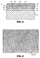
FIG. 2 is a cross-section side view of the insert ofFIG. 1 , taken along section lines 2-2. -
FIG. 3 is a micrograph of the surface of an exemplary optical element formed from polymer injection molded from a mold having an insert according to the present invention. - Patents, patent applications, and publications disclosed herein are hereby incorporated by reference (in their entirety) as if individually incorporated. It is to be understood that the above description is intended to be illustrative, and not restrictive. Various modifications and alterations of this invention will become apparent to those skilled in the art from the foregoing description without departing from the scope of this invention, and it should be understood that this invention is not to be unduly limited to the illustrative embodiments set forth herein.
- The present invention teaches how an adhesive may be used to bond elements so as to form an insert that can form part of an, e.g. injection mold. That this could be possible is not obvious; a thermoplastic injection mold undergoes rapid and drastic temperature cycling during its operation. Adhesives tend to be poor thermal conductors, and a layer of adhesive separating a stamping surface from the bulk of the thermal mass of the mold would seriously lengthen its cycle time. Furthermore, the integrity of the adhesive would usually quickly break down under such severe thermal stress.
- Referring now to
FIG. 1 , a perspective view of a surface of aninjection mold 10 including aninsert 12 according to the present invention is illustrated. The depictedmold 10 conveniently includes afirst mold portion 14 and asecond mold portion 16, although those skilled in the art will realize that a thermoplastic injection mold may have more than two major portions. First andsecond mold portion mold 10 byinput port 18. Optionally, themold 10 may be further cooled by the introduction of e.g. chilled water viacooling channels 20. Theinsert 12 is in contact with to firstmold portion body 22 in the depicted embodiment, but it will be understood that more than one mold portion may have an insert in other embodiments of the present invention. - Referring now to
FIG. 2 , a cross-section end view of themold 10 ofFIG. 1 , taken along section lines 2-2, is illustrated. In this view it can be more readily appreciated that theinsert 12 includes astamper 30 having animpression surface 32 and abacking surface 34. Theimpression surface 32 bears on itself a reverse of the pattern that is to be given to the polymeric part being molded by themold 10. It is not necessary that theimpression surface 32 be of a different material of thebacking surface 34, although it is frequently convenient that they be of different materials as will be discussed with more particularity below. - The
stamper 30 is supported by a support block 40, the support block 40 having a facingsurface 42 having a plurality ofprojections 44 thereon, the plurality ofprojections 44 being in contact with thebacking surface 34. A quantity ofadhesive 46 is disposed between theprojections 44 adhering the facingsurface 42 to thebacking surface 34. While theprojections 44 may have various geometries, it is usually convenient for theprojections 44 to have generally flatupper surfaces 48 for contacting thebacking surface 34. When theupper surfaces 48 are generally flat, it is particularly easy to insure that thestamper 30 is in proper position relative to firstmold portion body 22. It is also usually convenient for theprojections 44 to havesides 50 that are undercut with respect to the generally flatupper surfaces 48, the better to achieve adhesive bond with the adhesive 46. However, the invention is operable whethersides 50 of theprojections 44 have a draft that is negative, zero, or positive. - At least about 5% of the
backing surface 34 should be in contact with the flatupper surfaces 48 of theprojections 44. A trade-off is involved, since bonding between thestamper backing surface 34 to the support block 40 accomplished by the adhesive 46 and it needs surface area on thebacking surface 34 to accomplish this, but the transfer of heat away from thestamper 30 and into the support block 40 accomplished by theprojections 44 and they need surface area on thebacking surface 34 to accomplish that. It is believed that embodiments where between about 5 percent to 50 percent of thebacking surface 34 is in contact with the flatupper surfaces 48 of theprojections 44 are particularly suitable. Good results are achieved when between about 10 percent and 35 percent of thebacking surface 34 is in contact with the flatupper surfaces 48. - Good results are achieved when the
backing surface 34 and theprojections 44 have a certain amount of roughness. Such roughness allows a better holding surface for adhesive 46 to take a grip. It also provides microchannels for any adhesive that has been inadvertently placed on theupper surfaces 48 of theprojections 44 to be expelled as thestamper 32 is being mounted on the support block 40. A roughness of approximately 2.5 microns (rms) is believed to be suitable with an adhesive viscosity of approx 15,000 centipoise and an assembly force of approximately 12 Mpa. While it is believed that best results are achieved when theupper surfaces 48 are in direct contact with thebacking surface 34, it will be understood that it will not usually be convenient to totally exclude adhesive 46 from being between at least some of theupper surfaces 48 and thebacking surface 34. For the purposes of this application, the phrase, "the plurality of projections in contact with the backing surface" includes the possibility that some thin layer ofadhesive 46 may be present above some of theprojections 44, between them and thebacking surface 34. - A method for fabricating the
insert 12 begins with the step of fabricating astamper 32 having animpression surface 32 and abacking surface 34. One convenient way of fabricating astamper 32 begins with fabricating a master with a patterned surface. The master is conveniently prepared from diverse organic and inorganic materials using various techniques appropriate to each. For example, masters prepared from metals are conveniently shaped by methods such as machining, diamond turning, grinding, electroforming, ion beam etching electronic discharge machining (EDM) and the like. Masters prepared from polymers are conveniently shaped by photolithography, laser ablation, machining, diamond turning, or the like. - Next, what will soon be the
impression surface 32 is electroformed onto the patterned surface of the master. Nickel is often a most convenient impression surface, and both electrolytic and electrolcss processes are typically convenient for applying it. Then, optionally, what will soon become the backing surface is plated onto what will soon he the underside of the impression surface. Copper and copper alloys, because of their high thermal conductivity and good properties as a substrate for adhesive bonding, are often a most convenient backing surface, and an electrolytic process is typically convenient for applying it. Finally, the impression surface is separated from the patterned surface of the master. This is conveniently done by hand, possibly requiring the use of a knife's edge lightly at the interface between the master and the impression surface as a lever to begin the separation. - The method of making the insert then proceeds with the fabrication of the support block 40. The support block 40 is conveniently fabricated from copper or its alloys when it is desired to maximize heat removal from impression surface, but other metals such as steel may be used. The plurality of projections are conveniently created on the surface of e.g., a copper block, by various structuring methods commonly used in precision metal fabrication. It is believed that projections having a height between about 0.127 mm (0.005 inch) and 6.35 mm (0.250 inch) are workable. Good results have been achieved with projections with a height between about 0.127mm (0.005 inch) and 0.635 mm (0.025 inch). The support block 40 can be conveniently prepared from a single block of, e.g. copper metal, or it can be a composite as illustrated in
Fig. 2 , with theprojections 44 on asurface layer 50 supported by abase layer 52. - The backing surface is a then positioned in contact with the plurality of projections on what is now the facing surface of the support block. The stamper is adhered to the support block with a quantity of adhesive disposed between the projections. Different classes of adhesives may be used, depending on such factors as the temperature required to melt the material being molded, the molding rate, and the efficiency of the cooling system provided for the injection mold. For many of the applications contemplated for the present invention, adhesives such as epoxy adhesives and silicone adhesives may be used. Suitable adhesives include Scotch-Weld EC-3448 one-component epoxy and Scotch-Weld DP-420 two-component epoxy, both commercially available from 3M Company of St. Paul, MN. While the invention contemplates a lot of the heat transfer will occur through the projections, is also convenient to choose an adhesive with as much thermal transfer properties as can be achieved with the limitation of providing adequate bond strength and resistance to heat stress. One way of accomplishing this is the use of metal filled adhesives, and metal-filled high temperature epoxy resin systems are considered particularly useful. More particularly, the metal-filled high temperature epoxy resin system commercially available as 70-3810 from Epoxies, Etc. of Cranston, RI is considered suitable.
- It is possible, although not preferred, to embody the invention with projections on the backing surface, the projections contacting a generally flat facing surface. While such a thing would be more costly to fabricate without distorting the dimensional accuracy of the impression surface, it is considered within the scope of the invention.
- Inserts as described above can then be used in conventional injection molding to conveniently provide parts having fine detail. The inserts and method also lends itself to other molding and extruding operations such as, e.g. compression or blow molding. Cost savings are achieved because the inserts can be replaced at relatively low cost when the impression surface has become worn or the product design requires adjustment. It is contemplated that the present invention is particularly useful for making parts for optical interfaces and displays, for microelectronics and data storage products, for microbial detectors, for pharmaceutical delivery, and for tools suitable for genomics and proteomics.
- An insert for an injection mold according to the present invention was fabricated for the purpose of molding a backlight for a PDA. The backlight required was 64 mm by 68 mm by 1 mm, to be prepared from polymethyl methacrylate (PMMA), specifically formulation V825 commercially available from Atohaas N.A. of Bristol, PA. The backlight required a series of parallel ridges, trapezoidal in shape, having a width across the top of 17.8 microns, and being spaced approximately 100 to 150 microns apart. A photomicrograph of the completed backlight according to the rest of this example is illustrated in
Fig. 3 . - The shape for the backlight was machined in copper, 0.5 mm thick to form a master, and the master was chemically passivated. A layer of nickel was then electroformed onto the master by electrolytic plating, forming what was to be become the impression surface of a stamper. The layer of nickel had a thickness of about 500 microns.
- The plated master was then further treated by electroplating in a copper sulfate solution until layer of copper having a thickness of about 600 microns had been deposited on the nickel surface. The stamper, with its nickel impression surface and its copper backing surface, were then separated from the master with hand tension. As a final step, surface 34 (as seen in
fig. 2 ) was planarized. - A support block was then fabricated from PAS 940 copper alloy from Ampco Alloys. The flat surface of the copper alloy block was structured to create an array of raised projections, each projection having a height of about 0.38 mm (0.015 inch), and having a square upper surface, each side measuring about 0.25 mm (0.010 inch). The projections were arranged in a rectilinear array with a separation of about 0.51 mm (0.020 inch) between centers. The projections had a slight undercut of about 0.05 mm (0.002) inch on all four sides.
- The upper surfaces of the projections and the backing surface of the stamper were then treated with abrasive media to impart a surface roughness of about 2.5 microns. A quantity of a metal-filled high temperature epoxy resin system commercially available as 70-3810 from Epoxies, Etc. of Cranston, RI was then disposed upon the support block between the projections. The backing surface of the stamper was then adhered to the support block using the adhesive with the backing surface in firm contact with the upper surfaces of the projections to form the insert.
- The insert was then assembled into a mold portion body of a steel injection mold of otherwise conventional construction. The insert was provided with a shoulder on its side that fitted up against a corresponding ledge in the steel injection mold portion, and the insert was bolted in place. The injection mold was then connected to an extruder providing the polymethyl methacrylate at a temperature of 225 °C and an operating pressure of 60 Mpa. The injection mold was then operated using conventional techniques, forming the described backlights.
Claims (26)
- An insert (12) for a mold (10), comprising:a stamper (30) having an impression surface (32) and a backing surface (34);a support block (40) having a facing surface (42) having a plurality of projection (44) thereon, the plurality of projections (44) in contact with the backing surface (34), andan adhesive (46) disposed between the sides of the projection (44) for adhering the facing surface (42) to the backing surface (34).
- The insert (12) according to claim 1 wherein the projections (44) have generally flat upper surfaces (48) for contacting the backing surface (34) and wherein between about 5% to 50% of the backing surface (34) is in contact with the generally flat upper surface (48).
- The insert (12) according to claim 2 wherein between about 10% to 35% of the backing surface (34) is in contact with the flat upper surface (48).
- The insert (12) according to claim 2 wherein at least a portion of the sides of the projections (44) are undercut with respect to the generally flat upper surfaces (48).
- The insert (12) according to claim 1 wherein the stamper (30) is a composite construction such that the impression surface (32) and the backing surface (34) are comprised of different materials.
- The insert (12) according to claim 5 wherein the impression surface (32) is selected from the group consisting of nickel and nickel alloys.
- The insert (12) according to claim 5 wherein the backing surface (34) is selected from the group consisting of copper and copper alloys.
- The insert (12) according to claim 1 wherein the projections (44) are made from a material selected from the group consisting of copper, copper alloys, iron, steel and aluminum.
- The insert (12) according to claim 1 wherein the adhesive (46) is selected from the group consisting of epoxy adhesives and silicone adhesives.
- The insert (12) according to claim 9 wherein the adhesive (46) is a metal-filled high temperature epoxy resin system.
- The insert (12) according to claim 1 wherein the projections (44) have a height between about 0.127 mm and 6.35 mm.
- The insert (12) according to claim 11 wherein the projection (44) have a height between about 0.127mm and 0.635 mm.
- The insert (12) according to claim 1 wherein the insert (12) is adapted for an injection mold.
- A method for fabricating an insert for a mold, the method comprising:fabricating a stamper (30) having an impression surface (32) and a backing surface (34);fabricating a support block (40) having a facing surface (42) having a plurality of projections (44) thereon;positioning the backing surface (34) in contact with the plurality of projections (44); andadhering the stamper (30) to the support with a quantity of adhesive (46) disposed between the sides of the projections (44).
- The method according to claim 14 wherein the projections (44) have generally flat upper surfaces (48) for contacting the backing surface (34), and wherein at least about 5% and 50% of the backing surface is in contact with the flat upper surfaces.
- The method according to claim 15 further comprising the step of undercutting at least a portion of the sides of the projections (44) with respect to the generally flat upper surfaces (48).
- The method according to claim 14 wherein the step of fabricating a stamper comprises
fabricating a master such that the master has a patterned surface;
electroforming the impression surface onto the patterned surface;
plating the backing surface (34) onto the impression surface (32); and
separating the impression surface (32) from the patterned surface. - The method according to claim 17 wherein the step of fabricating a stamper comprises
treating the patterned surface with a passivating substance. - The method according to claim of 14 wherein the impression surface (32) is selected from the group consisting of nickel and nickel alloys.
- The method according to claim 14 wherein the backing surface (34) is selected from the group consisting of copper and copper alloys.
- The method according to claim 14 wherein the projections (44) are made from a material selected from the group consisting of copper, copper alloys, iron and steel, and aluminum.
- The method according to claim 14 wherein the adhesive is selected from the group consisting of epoxy adhesives and silicone adhesives.
- The method according to claim 22 wherein the adhesive is a metal-filled high temperature epoxy resin system.
- The method according to claim 14 wherein the projections have a height between about 0.127 mm and 6.35 mm.
- The method according to claim 24 wherein the projections have a height between about 0.127 mm and 0.635 mm.
- An insert (12) for a mold, comprising:a stamper (30) having an impression surface (32) and a backing surface (34);a support block (40) having a facing surface (42);a plurality of projections (44) on the backing surface (34), or on the backing surface and the support surface, the plurality of projections (44) in contact with the other of the backing surface (34) and the support surface; andan adhesive (46) disposed between the sides of the projections (44) for adhering the facing surface to the backing surface (34). .
Applications Claiming Priority (3)
| Application Number | Priority Date | Filing Date | Title |
|---|---|---|---|
| US329837 | 2002-12-26 | ||
| US10/329,837 US6939123B2 (en) | 2002-12-26 | 2002-12-26 | Electroformed adhesive laminated tooling surface with precision structured interfaces |
| PCT/US2003/036098 WO2004060632A1 (en) | 2002-12-26 | 2003-11-12 | Electroformed adhesive laminated tooling surface with precision structured interfaces |
Publications (2)
| Publication Number | Publication Date |
|---|---|
| EP1578582A1 EP1578582A1 (en) | 2005-09-28 |
| EP1578582B1 true EP1578582B1 (en) | 2011-12-21 |
Family
ID=32654367
Family Applications (1)
| Application Number | Title | Priority Date | Filing Date |
|---|---|---|---|
| EP03781916A Expired - Lifetime EP1578582B1 (en) | 2002-12-26 | 2003-11-12 | Electroformed adhesive laminated tooling surface with precision structured interfaces |
Country Status (9)
| Country | Link |
|---|---|
| US (1) | US6939123B2 (en) |
| EP (1) | EP1578582B1 (en) |
| JP (1) | JP4607599B2 (en) |
| KR (1) | KR101004830B1 (en) |
| AT (1) | ATE537955T1 (en) |
| AU (1) | AU2003287711A1 (en) |
| BR (1) | BR0317670A (en) |
| MX (1) | MXPA05006667A (en) |
| WO (1) | WO2004060632A1 (en) |
Families Citing this family (11)
| Publication number | Priority date | Publication date | Assignee | Title |
|---|---|---|---|---|
| KR100442874B1 (en) * | 2002-03-25 | 2004-08-02 | 삼성전자주식회사 | Actuator for hard disk drive |
| DE10328046A1 (en) * | 2003-06-23 | 2005-01-13 | Arvinmeritor Gmbh | Method for producing a plastic composite component, in particular a body component |
| US7121155B2 (en) * | 2004-12-29 | 2006-10-17 | 3M Innovative Properties Company | Pressure indicating structure |
| KR100807186B1 (en) * | 2005-11-29 | 2008-02-28 | 전자부품연구원 | Method for manufacturing an integrated stamper mold for injection molding of light grid panel |
| JP2007168205A (en) * | 2005-12-21 | 2007-07-05 | Toshin Seiko:Kk | Mold and method for producing block |
| US8403659B2 (en) * | 2006-08-02 | 2013-03-26 | Robert E. Szokolay | Mold tooling with integrated thermal management fluid channels and method |
| ES2579228T3 (en) * | 2008-07-25 | 2016-08-08 | Sika Technology Ag | Interconnected foam or adhesive layers |
| PL2248615T3 (en) * | 2009-05-05 | 2014-04-30 | Meissner Formentechnologie Gmbh | Temperable tool and use of the same |
| KR20120115617A (en) | 2011-04-11 | 2012-10-19 | 삼성디스플레이 주식회사 | Stamper and method of manufacturing the same |
| CN107987483B (en) * | 2017-12-26 | 2020-11-03 | 天津康普斯特科技发展有限公司 | Method for quickly manufacturing injection mold |
| CN110000528B (en) * | 2019-04-22 | 2020-04-28 | 浙江靓鸿新材料有限公司 | Preparation method of manufacturing mold of photocuring microprism of reflective film |
Family Cites Families (17)
| Publication number | Priority date | Publication date | Assignee | Title |
|---|---|---|---|---|
| US4285901A (en) | 1978-07-06 | 1981-08-25 | Akira Yotsutsuji | Method of making an insulated metal mold |
| JPS58185049A (en) | 1982-04-22 | 1983-10-28 | Hitachi Ltd | Stamper and its production |
| JPS60149422A (en) | 1984-01-18 | 1985-08-06 | Matsushita Electric Ind Co Ltd | Manufacture of digital signal recording and regenerating disc |
| JPS62167639A (en) * | 1985-09-13 | 1987-07-24 | Fujitsu Ltd | Production of optical disk transfer mold |
| JPH0268744A (en) | 1988-09-05 | 1990-03-08 | Sumitomo Bakelite Co Ltd | Method for backing stamper |
| JPH0322230A (en) * | 1989-06-20 | 1991-01-30 | Nikka Eng Kk | Stamper and manufacture of the same |
| ES2091810T3 (en) * | 1989-08-07 | 1996-11-16 | Nissan Motor | EPOXY RESIN MOLD FILLED WITH METALLIC POWDER AND METHOD FOR ITS MANUFACTURE. |
| JPH04131211A (en) | 1990-09-21 | 1992-05-01 | Toshiba Mach Co Ltd | Plastic lens manufacture and manufacturing mold |
| JP3006199B2 (en) * | 1991-09-03 | 2000-02-07 | 株式会社日立製作所 | Optical disc manufacturing method |
| JPH05200755A (en) * | 1992-01-24 | 1993-08-10 | Olympus Optical Co Ltd | Production of electroformed mold |
| US5702735A (en) | 1994-06-10 | 1997-12-30 | Johnson & Johnson Vision Products, Inc. | Molding arrangement to achieve short mold cycle time |
| JPH09300359A (en) | 1996-05-08 | 1997-11-25 | Kojima Press Co Ltd | Rapid heating mold and its production |
| JPH10315273A (en) | 1997-05-15 | 1998-12-02 | Sony Corp | Production equipment of board for disk and stamper used therein |
| US6354827B1 (en) | 1998-11-12 | 2002-03-12 | Imation Corp. | Stamper assembly for manufacturing optical data storage disks |
| JP3104699B1 (en) * | 1999-06-01 | 2000-10-30 | 株式会社ニコン | Manufacturing method of molded substrate with fine grooves |
| DE19933530C5 (en) | 1999-07-16 | 2014-04-17 | Bayerische Motoren Werke Aktiengesellschaft | Injection mold for the production of plastic moldings |
| DE50001604D1 (en) * | 2000-01-27 | 2003-05-08 | Awm Mold Tech Ag Muri | Injection molding tool for the production of disc-shaped information carriers |
-
2002
- 2002-12-26 US US10/329,837 patent/US6939123B2/en not_active Expired - Lifetime
-
2003
- 2003-11-12 AU AU2003287711A patent/AU2003287711A1/en not_active Abandoned
- 2003-11-12 MX MXPA05006667A patent/MXPA05006667A/en active IP Right Grant
- 2003-11-12 WO PCT/US2003/036098 patent/WO2004060632A1/en active Application Filing
- 2003-11-12 BR BR0317670-3A patent/BR0317670A/en not_active IP Right Cessation
- 2003-11-12 JP JP2004564972A patent/JP4607599B2/en not_active Expired - Fee Related
- 2003-11-12 KR KR1020057011930A patent/KR101004830B1/en not_active IP Right Cessation
- 2003-11-12 AT AT03781916T patent/ATE537955T1/en active
- 2003-11-12 EP EP03781916A patent/EP1578582B1/en not_active Expired - Lifetime
Also Published As
| Publication number | Publication date |
|---|---|
| US20040126455A1 (en) | 2004-07-01 |
| MXPA05006667A (en) | 2005-09-30 |
| AU2003287711A1 (en) | 2004-07-29 |
| EP1578582A1 (en) | 2005-09-28 |
| JP2006512231A (en) | 2006-04-13 |
| KR101004830B1 (en) | 2010-12-28 |
| KR20050088327A (en) | 2005-09-05 |
| ATE537955T1 (en) | 2012-01-15 |
| BR0317670A (en) | 2005-11-29 |
| US6939123B2 (en) | 2005-09-06 |
| JP4607599B2 (en) | 2011-01-05 |
| WO2004060632A1 (en) | 2004-07-22 |
Similar Documents
| Publication | Publication Date | Title |
|---|---|---|
| EP1578582B1 (en) | Electroformed adhesive laminated tooling surface with precision structured interfaces | |
| US6660151B1 (en) | Microstructure elements and process for the production thereof | |
| EP1342559B1 (en) | Method of fabricating an injection mould insert for contact lens moulds and injection mould insert | |
| US5705256A (en) | Method for fabricating optical quality molds with precision microfeatures | |
| US5543108A (en) | Method of making microstructured bodies of plastic material | |
| Zhang et al. | Performance of nickel and bulk metallic glass as tool inserts for the microinjection molding of polymeric microfluidic devices | |
| US4707904A (en) | Method of manufacturing a die for extruding honeycomb body | |
| US7731830B2 (en) | Mold tooling with integrated conformal thermal management fluid channels and method | |
| CN114101475B (en) | Ultrasonic imprinting forming method and forming equipment for high-temperature and high-Jiang Fei crystal alloy micro-die | |
| US7195862B2 (en) | Process for producing a tool insert for injection molding a microstructured part | |
| US20110070122A1 (en) | Alloy Composition | |
| CN104552679A (en) | Preparation method of mold core of mold, mold core of mold and biochip | |
| Hansen et al. | Tooling process chains and concepts | |
| JP2006068998A (en) | Work cutting fixing tool and cutting method using the same | |
| JP6124023B2 (en) | Mold for molding and manufacturing method thereof | |
| CN1739912A (en) | Molding process | |
| JP2008246714A (en) | Mold part manufacturing method and mold part | |
| EP1602623B1 (en) | Method of moulding a microfluidic structure and mould | |
| US8403659B2 (en) | Mold tooling with integrated thermal management fluid channels and method | |
| CN216100140U (en) | Center block for preventing slitter edge from sticking to mold in injection mold | |
| US20080029397A1 (en) | Hot embossing tooling with integrated heating/cooling fluid channels and method | |
| EP1884337A1 (en) | Disc molding mold, mirror-surface disc, and method for producing mold for disc molding | |
| KR20050038721A (en) | Manufacturing method for superbright mold | |
| Tang et al. | Electroforming of Tool Inserts for Injection Molding of Optical or Microfluidic Components | |
| WO1999003100A1 (en) | Method of manufacturing a master disc unit and a matrix produced therefrom and adapter ring for manufacturing the master disc unit |
Legal Events
| Date | Code | Title | Description |
|---|---|---|---|
| PUAI | Public reference made under article 153(3) epc to a published international application that has entered the european phase |
Free format text: ORIGINAL CODE: 0009012 |
|
| 17P | Request for examination filed |
Effective date: 20050719 |
|
| AK | Designated contracting states |
Kind code of ref document: A1 Designated state(s): AT BE BG CH CY CZ DE DK EE ES FI FR GB GR HU IE IT LI LU MC NL PT RO SE SI SK TR |
|
| AX | Request for extension of the european patent |
Extension state: AL LT LV MK |
|
| DAX | Request for extension of the european patent (deleted) | ||
| 17Q | First examination report despatched |
Effective date: 20070920 |
|
| GRAP | Despatch of communication of intention to grant a patent |
Free format text: ORIGINAL CODE: EPIDOSNIGR1 |
|
| GRAS | Grant fee paid |
Free format text: ORIGINAL CODE: EPIDOSNIGR3 |
|
| GRAA | (expected) grant |
Free format text: ORIGINAL CODE: 0009210 |
|
| AK | Designated contracting states |
Kind code of ref document: B1 Designated state(s): AT BE BG CH CY CZ DE DK EE ES FI FR GB GR HU IE IT LI LU MC NL PT RO SE SI SK TR |
|
| REG | Reference to a national code |
Ref country code: GB Ref legal event code: FG4D |
|
| REG | Reference to a national code |
Ref country code: CH Ref legal event code: EP |
|
| REG | Reference to a national code |
Ref country code: AT Ref legal event code: REF Ref document number: 537955 Country of ref document: AT Kind code of ref document: T Effective date: 20120115 |
|
| REG | Reference to a national code |
Ref country code: IE Ref legal event code: FG4D |
|
| REG | Reference to a national code |
Ref country code: DE Ref legal event code: R096 Ref document number: 60339503 Country of ref document: DE Effective date: 20120301 |
|
| REG | Reference to a national code |
Ref country code: NL Ref legal event code: VDEP Effective date: 20111221 |
|
| PG25 | Lapsed in a contracting state [announced via postgrant information from national office to epo] |
Ref country code: GR Free format text: LAPSE BECAUSE OF FAILURE TO SUBMIT A TRANSLATION OF THE DESCRIPTION OR TO PAY THE FEE WITHIN THE PRESCRIBED TIME-LIMIT Effective date: 20120322 Ref country code: NL Free format text: LAPSE BECAUSE OF FAILURE TO SUBMIT A TRANSLATION OF THE DESCRIPTION OR TO PAY THE FEE WITHIN THE PRESCRIBED TIME-LIMIT Effective date: 20111221 Ref country code: SE Free format text: LAPSE BECAUSE OF FAILURE TO SUBMIT A TRANSLATION OF THE DESCRIPTION OR TO PAY THE FEE WITHIN THE PRESCRIBED TIME-LIMIT Effective date: 20111221 Ref country code: SI Free format text: LAPSE BECAUSE OF FAILURE TO SUBMIT A TRANSLATION OF THE DESCRIPTION OR TO PAY THE FEE WITHIN THE PRESCRIBED TIME-LIMIT Effective date: 20111221 |
|
| PG25 | Lapsed in a contracting state [announced via postgrant information from national office to epo] |
Ref country code: BE Free format text: LAPSE BECAUSE OF FAILURE TO SUBMIT A TRANSLATION OF THE DESCRIPTION OR TO PAY THE FEE WITHIN THE PRESCRIBED TIME-LIMIT Effective date: 20111221 Ref country code: CY Free format text: LAPSE BECAUSE OF FAILURE TO SUBMIT A TRANSLATION OF THE DESCRIPTION OR TO PAY THE FEE WITHIN THE PRESCRIBED TIME-LIMIT Effective date: 20111221 |
|
| PG25 | Lapsed in a contracting state [announced via postgrant information from national office to epo] |
Ref country code: BG Free format text: LAPSE BECAUSE OF FAILURE TO SUBMIT A TRANSLATION OF THE DESCRIPTION OR TO PAY THE FEE WITHIN THE PRESCRIBED TIME-LIMIT Effective date: 20120321 Ref country code: CZ Free format text: LAPSE BECAUSE OF FAILURE TO SUBMIT A TRANSLATION OF THE DESCRIPTION OR TO PAY THE FEE WITHIN THE PRESCRIBED TIME-LIMIT Effective date: 20111221 Ref country code: EE Free format text: LAPSE BECAUSE OF FAILURE TO SUBMIT A TRANSLATION OF THE DESCRIPTION OR TO PAY THE FEE WITHIN THE PRESCRIBED TIME-LIMIT Effective date: 20111221 Ref country code: SK Free format text: LAPSE BECAUSE OF FAILURE TO SUBMIT A TRANSLATION OF THE DESCRIPTION OR TO PAY THE FEE WITHIN THE PRESCRIBED TIME-LIMIT Effective date: 20111221 |
|
| PG25 | Lapsed in a contracting state [announced via postgrant information from national office to epo] |
Ref country code: RO Free format text: LAPSE BECAUSE OF FAILURE TO SUBMIT A TRANSLATION OF THE DESCRIPTION OR TO PAY THE FEE WITHIN THE PRESCRIBED TIME-LIMIT Effective date: 20111221 Ref country code: PT Free format text: LAPSE BECAUSE OF FAILURE TO SUBMIT A TRANSLATION OF THE DESCRIPTION OR TO PAY THE FEE WITHIN THE PRESCRIBED TIME-LIMIT Effective date: 20120423 |
|
| REG | Reference to a national code |
Ref country code: AT Ref legal event code: MK05 Ref document number: 537955 Country of ref document: AT Kind code of ref document: T Effective date: 20111221 |
|
| PLBE | No opposition filed within time limit |
Free format text: ORIGINAL CODE: 0009261 |
|
| STAA | Information on the status of an ep patent application or granted ep patent |
Free format text: STATUS: NO OPPOSITION FILED WITHIN TIME LIMIT |
|
| PG25 | Lapsed in a contracting state [announced via postgrant information from national office to epo] |
Ref country code: DK Free format text: LAPSE BECAUSE OF FAILURE TO SUBMIT A TRANSLATION OF THE DESCRIPTION OR TO PAY THE FEE WITHIN THE PRESCRIBED TIME-LIMIT Effective date: 20111221 |
|
| 26N | No opposition filed |
Effective date: 20120924 |
|
| PG25 | Lapsed in a contracting state [announced via postgrant information from national office to epo] |
Ref country code: IT Free format text: LAPSE BECAUSE OF FAILURE TO SUBMIT A TRANSLATION OF THE DESCRIPTION OR TO PAY THE FEE WITHIN THE PRESCRIBED TIME-LIMIT Effective date: 20111221 |
|
| REG | Reference to a national code |
Ref country code: DE Ref legal event code: R097 Ref document number: 60339503 Country of ref document: DE Effective date: 20120924 |
|
| PG25 | Lapsed in a contracting state [announced via postgrant information from national office to epo] |
Ref country code: AT Free format text: LAPSE BECAUSE OF FAILURE TO SUBMIT A TRANSLATION OF THE DESCRIPTION OR TO PAY THE FEE WITHIN THE PRESCRIBED TIME-LIMIT Effective date: 20111221 |
|
| PG25 | Lapsed in a contracting state [announced via postgrant information from national office to epo] |
Ref country code: ES Free format text: LAPSE BECAUSE OF FAILURE TO SUBMIT A TRANSLATION OF THE DESCRIPTION OR TO PAY THE FEE WITHIN THE PRESCRIBED TIME-LIMIT Effective date: 20120401 |
|
| PG25 | Lapsed in a contracting state [announced via postgrant information from national office to epo] |
Ref country code: FI Free format text: LAPSE BECAUSE OF FAILURE TO SUBMIT A TRANSLATION OF THE DESCRIPTION OR TO PAY THE FEE WITHIN THE PRESCRIBED TIME-LIMIT Effective date: 20111221 |
|
| REG | Reference to a national code |
Ref country code: CH Ref legal event code: PL |
|
| GBPC | Gb: european patent ceased through non-payment of renewal fee |
Effective date: 20121112 |
|
| PG25 | Lapsed in a contracting state [announced via postgrant information from national office to epo] |
Ref country code: CH Free format text: LAPSE BECAUSE OF NON-PAYMENT OF DUE FEES Effective date: 20121130 Ref country code: LI Free format text: LAPSE BECAUSE OF NON-PAYMENT OF DUE FEES Effective date: 20121130 |
|
| REG | Reference to a national code |
Ref country code: IE Ref legal event code: MM4A |
|
| REG | Reference to a national code |
Ref country code: FR Ref legal event code: ST Effective date: 20130731 |
|
| PG25 | Lapsed in a contracting state [announced via postgrant information from national office to epo] |
Ref country code: IE Free format text: LAPSE BECAUSE OF NON-PAYMENT OF DUE FEES Effective date: 20121112 |
|
| PG25 | Lapsed in a contracting state [announced via postgrant information from national office to epo] |
Ref country code: FR Free format text: LAPSE BECAUSE OF NON-PAYMENT OF DUE FEES Effective date: 20121130 Ref country code: GB Free format text: LAPSE BECAUSE OF NON-PAYMENT OF DUE FEES Effective date: 20121112 |
|
| PG25 | Lapsed in a contracting state [announced via postgrant information from national office to epo] |
Ref country code: TR Free format text: LAPSE BECAUSE OF FAILURE TO SUBMIT A TRANSLATION OF THE DESCRIPTION OR TO PAY THE FEE WITHIN THE PRESCRIBED TIME-LIMIT Effective date: 20111221 Ref country code: MC Free format text: LAPSE BECAUSE OF NON-PAYMENT OF DUE FEES Effective date: 20121130 |
|
| PG25 | Lapsed in a contracting state [announced via postgrant information from national office to epo] |
Ref country code: LU Free format text: LAPSE BECAUSE OF NON-PAYMENT OF DUE FEES Effective date: 20121112 |
|
| PG25 | Lapsed in a contracting state [announced via postgrant information from national office to epo] |
Ref country code: HU Free format text: LAPSE BECAUSE OF FAILURE TO SUBMIT A TRANSLATION OF THE DESCRIPTION OR TO PAY THE FEE WITHIN THE PRESCRIBED TIME-LIMIT Effective date: 20031112 |
|
| PGFP | Annual fee paid to national office [announced via postgrant information from national office to epo] |
Ref country code: DE Payment date: 20171108 Year of fee payment: 15 |
|
| REG | Reference to a national code |
Ref country code: DE Ref legal event code: R119 Ref document number: 60339503 Country of ref document: DE |
|
| PG25 | Lapsed in a contracting state [announced via postgrant information from national office to epo] |
Ref country code: DE Free format text: LAPSE BECAUSE OF NON-PAYMENT OF DUE FEES Effective date: 20190601 |