EP1577952A1 - High voltage insulated gate field-effect transistor and method of making the same - Google Patents
High voltage insulated gate field-effect transistor and method of making the same Download PDFInfo
- Publication number
- EP1577952A1 EP1577952A1 EP04100960A EP04100960A EP1577952A1 EP 1577952 A1 EP1577952 A1 EP 1577952A1 EP 04100960 A EP04100960 A EP 04100960A EP 04100960 A EP04100960 A EP 04100960A EP 1577952 A1 EP1577952 A1 EP 1577952A1
- Authority
- EP
- European Patent Office
- Prior art keywords
- region
- insulated
- drain region
- trench
- gate
- Prior art date
- Legal status (The legal status is an assumption and is not a legal conclusion. Google has not performed a legal analysis and makes no representation as to the accuracy of the status listed.)
- Granted
Links
Images



Classifications
-
- H—ELECTRICITY
- H10—SEMICONDUCTOR DEVICES; ELECTRIC SOLID-STATE DEVICES NOT OTHERWISE PROVIDED FOR
- H10D—INORGANIC ELECTRIC SEMICONDUCTOR DEVICES
- H10D62/00—Semiconductor bodies, or regions thereof, of devices having potential barriers
- H10D62/01—Manufacture or treatment
- H10D62/021—Forming source or drain recesses by etching e.g. recessing by etching and then refilling
-
- H—ELECTRICITY
- H10—SEMICONDUCTOR DEVICES; ELECTRIC SOLID-STATE DEVICES NOT OTHERWISE PROVIDED FOR
- H10D—INORGANIC ELECTRIC SEMICONDUCTOR DEVICES
- H10D30/00—Field-effect transistors [FET]
- H10D30/01—Manufacture or treatment
- H10D30/021—Manufacture or treatment of FETs having insulated gates [IGFET]
- H10D30/028—Manufacture or treatment of FETs having insulated gates [IGFET] of double-diffused metal oxide semiconductor [DMOS] FETs
- H10D30/0281—Manufacture or treatment of FETs having insulated gates [IGFET] of double-diffused metal oxide semiconductor [DMOS] FETs of lateral DMOS [LDMOS] FETs
-
- H—ELECTRICITY
- H10—SEMICONDUCTOR DEVICES; ELECTRIC SOLID-STATE DEVICES NOT OTHERWISE PROVIDED FOR
- H10D—INORGANIC ELECTRIC SEMICONDUCTOR DEVICES
- H10D30/00—Field-effect transistors [FET]
- H10D30/01—Manufacture or treatment
- H10D30/021—Manufacture or treatment of FETs having insulated gates [IGFET]
- H10D30/028—Manufacture or treatment of FETs having insulated gates [IGFET] of double-diffused metal oxide semiconductor [DMOS] FETs
- H10D30/0281—Manufacture or treatment of FETs having insulated gates [IGFET] of double-diffused metal oxide semiconductor [DMOS] FETs of lateral DMOS [LDMOS] FETs
- H10D30/0287—Manufacture or treatment of FETs having insulated gates [IGFET] of double-diffused metal oxide semiconductor [DMOS] FETs of lateral DMOS [LDMOS] FETs using recessing of the source electrodes
-
- H—ELECTRICITY
- H10—SEMICONDUCTOR DEVICES; ELECTRIC SOLID-STATE DEVICES NOT OTHERWISE PROVIDED FOR
- H10D—INORGANIC ELECTRIC SEMICONDUCTOR DEVICES
- H10D30/00—Field-effect transistors [FET]
- H10D30/60—Insulated-gate field-effect transistors [IGFET]
- H10D30/64—Double-diffused metal-oxide semiconductor [DMOS] FETs
- H10D30/65—Lateral DMOS [LDMOS] FETs
-
- H—ELECTRICITY
- H10—SEMICONDUCTOR DEVICES; ELECTRIC SOLID-STATE DEVICES NOT OTHERWISE PROVIDED FOR
- H10D—INORGANIC ELECTRIC SEMICONDUCTOR DEVICES
- H10D62/00—Semiconductor bodies, or regions thereof, of devices having potential barriers
- H10D62/10—Shapes, relative sizes or dispositions of the regions of the semiconductor bodies; Shapes of the semiconductor bodies
- H10D62/13—Semiconductor regions connected to electrodes carrying current to be rectified, amplified or switched, e.g. source or drain regions
- H10D62/149—Source or drain regions of field-effect devices
- H10D62/151—Source or drain regions of field-effect devices of IGFETs
- H10D62/152—Source regions of DMOS transistors
- H10D62/153—Impurity concentrations or distributions
-
- H—ELECTRICITY
- H10—SEMICONDUCTOR DEVICES; ELECTRIC SOLID-STATE DEVICES NOT OTHERWISE PROVIDED FOR
- H10D—INORGANIC ELECTRIC SEMICONDUCTOR DEVICES
- H10D62/00—Semiconductor bodies, or regions thereof, of devices having potential barriers
- H10D62/10—Shapes, relative sizes or dispositions of the regions of the semiconductor bodies; Shapes of the semiconductor bodies
- H10D62/13—Semiconductor regions connected to electrodes carrying current to be rectified, amplified or switched, e.g. source or drain regions
- H10D62/149—Source or drain regions of field-effect devices
- H10D62/151—Source or drain regions of field-effect devices of IGFETs
- H10D62/156—Drain regions of DMOS transistors
- H10D62/157—Impurity concentrations or distributions
-
- H—ELECTRICITY
- H10—SEMICONDUCTOR DEVICES; ELECTRIC SOLID-STATE DEVICES NOT OTHERWISE PROVIDED FOR
- H10D—INORGANIC ELECTRIC SEMICONDUCTOR DEVICES
- H10D64/00—Electrodes of devices having potential barriers
- H10D64/20—Electrodes characterised by their shapes, relative sizes or dispositions
- H10D64/23—Electrodes carrying the current to be rectified, amplified, oscillated or switched, e.g. sources, drains, anodes or cathodes
- H10D64/251—Source or drain electrodes for field-effect devices
- H10D64/256—Source or drain electrodes for field-effect devices for lateral devices wherein the source or drain electrodes are recessed in semiconductor bodies
-
- H—ELECTRICITY
- H10—SEMICONDUCTOR DEVICES; ELECTRIC SOLID-STATE DEVICES NOT OTHERWISE PROVIDED FOR
- H10P—GENERIC PROCESSES OR APPARATUS FOR THE MANUFACTURE OR TREATMENT OF DEVICES COVERED BY CLASS H10
- H10P30/00—Ion implantation into wafers, substrates or parts of devices
- H10P30/20—Ion implantation into wafers, substrates or parts of devices into semiconductor materials, e.g. for doping
- H10P30/222—Ion implantation into wafers, substrates or parts of devices into semiconductor materials, e.g. for doping characterised by the angle between the ion beam and the crystal planes or the main crystal surface
-
- H—ELECTRICITY
- H10—SEMICONDUCTOR DEVICES; ELECTRIC SOLID-STATE DEVICES NOT OTHERWISE PROVIDED FOR
- H10D—INORGANIC ELECTRIC SEMICONDUCTOR DEVICES
- H10D62/00—Semiconductor bodies, or regions thereof, of devices having potential barriers
- H10D62/80—Semiconductor bodies, or regions thereof, of devices having potential barriers characterised by the materials
- H10D62/83—Semiconductor bodies, or regions thereof, of devices having potential barriers characterised by the materials being Group IV materials, e.g. B-doped Si or undoped Ge
-
- H—ELECTRICITY
- H10—SEMICONDUCTOR DEVICES; ELECTRIC SOLID-STATE DEVICES NOT OTHERWISE PROVIDED FOR
- H10D—INORGANIC ELECTRIC SEMICONDUCTOR DEVICES
- H10D64/00—Electrodes of devices having potential barriers
- H10D64/60—Electrodes characterised by their materials
- H10D64/62—Electrodes ohmically coupled to a semiconductor
Definitions
- the present invention relates, in general, to semiconductor devices, and more particularly, to high-voltage insulated-gate (e.g., Metal Oxide Semiconductor) Field Effect Transistors (shortly, MOSFETs). More specifically, the invention relates to a Double-Diffused MOS (shortly, DMOS) field effect transistor (a DMOSFET) adapted to handling high voltages.
- insulated-gate e.g., Metal Oxide Semiconductor
- MOSFETs Metal Oxide Semiconductor Field Effect Transistors
- MOSFETs capable of sustaining high voltages ranging from 3 V to about 100 V and driving large currents ranging from 100 mA to about 1 A.
- MOSFETs capable of sustaining high voltages ranging from 3 V to about 100 V and driving large currents ranging from 100 mA to about 1 A.
- the main problem is the risk of depressing other electrical characteristics of the device such as, for example, a low internal resistance, which are as much important as the capability of handling high power.
- transistors for high voltage applications have to satisfy the existing demand for compact circuits, that continually steers the microelectronics industry into submicron regions and thin-oxide circuits.
- a DMOSFET is an enhancement-mode MOS transistor having a good punch-through control, which is reached by the provision of a double diffusion of dopants through the source diffusion window.
- two successive diffusions of dopants of opposite type are performed through the source diffusion window in a lightly doped substrate.
- a portion of the first diffusion underlies a gate oxide layer and acts as body region, within which the channel zone for the transistor conduction current forms.
- the second diffusion behaves as source region and the exploited dopants are of the same type as the dopants diffused to form the drain region.
- the main limitations for high voltage transistors are due to the electrical tolerances of the gate oxide layer, overlapping the channel region.
- the high electric field at the interface between the semiconductor and the gate oxide layer makes the transistor particularly sensitive to defects and accidental, but inevitable, contaminations of the oxide layer during manufacturing.
- the oxide/semiconductor interface close to said edge portion undergoes a degradation; such a degradation is more evident for devices having relatively thin gate oxide layers, which consequently suffer from significant unreliability when operating at relatively high drain voltages.
- the DMOS transistors can exploit an additional lightly doped region extending from the drain region to the gate and possibly from the source region to the gate, to introduce a voltage drop between the drain and source regions and the edge of the channel, reducing the electric field across the thin gate oxide layer.
- the electric field reduction achieved by the provision of these lightly doped regions may not be sufficient to avoid degradation of the gate oxide.
- US 5,430,316 discloses a DMOS transistor having a further region formed under the edge portion of the gate oxide adjacent to the drain region and doped with dopants of the same type as the body region dopants. This further region forces the conduction current to move away from the surface of the device down towards a buried silicon layer, before being collected by a sinker at the drain region.
- V-shaped and U-shaped grooved MOS transistors have been proposed, such as the Schottky-barrier vertical MOS transistor described in US 4,983,535.
- the dopants distribution is equivalent to that of a DMOS transistor, but a trench is etched to fully penetrate the body region, and the trench surfaces oxidized to form the gate oxide; the trench is filled with polysilicon, forming the gate electrode.
- the conduction current of the device flows parallel to walls of the etched trench and a common drain contact is provided at the bottom of the device, inducing a vertical conduction current.
- U.S. 6,093,588 discloses a high voltage MOS transistor in which, in order to save silicon area and reduce the specific internal resistance, drain regions are formed by implanting doping species into the silicon through apertures in the field oxide.
- U.S. 5,385,852 and U.S. 6,437,399 trenches are etched perpendicular to the surface of a substrate, to establish electrical contacts for reducing the transistor size and for improving the control of parasitic transistors.
- U.S 5,356,822 discloses complementary DMOS transistors in which trenches are etched in a silicon layer for electrically isolating N and P regions on which gates are formed.
- an insulated-gate transistor as set out in the appended claim 1 is proposed.
- the proposed insulated-gate transistor includes: a semiconductor material layer having a front surface; a body region of a first conductivity type formed in the semiconductor material layer in correspondence of the front surface; an insulated gate insulatively disposed over the body region with interposition of a gate dielectric; and a source region and a drain region of a second conductivity type opposite to the first conductivity type, the source region being formed in the body region and the drain region being formed in the semiconductor material layer, the source and the drain region being spaced apart from each other by: a channel zone in a portion of the body region underlying the insulated gate, and a charge carriers drift portion of the semiconductor material layer between the channel zone and the drain region, the insulated gate extending over the charge carriers drift portion, wherein the drain region is located at a depth compared to the front surface, for causing charge carriers to move in the charge carriers drift portion away from an interface between the semiconductor material layer and the gate dielectric.
- an integrated circuit as set forth in claim 14 is provided, including at least one of those insulated-gate transistors; according to still another aspect, a corresponding process for the fabrication of that insulated-gate transistor as set forth in claim 15 is also encompassed.
- a sectional view of a portion of an N-channel DMOS transistor 100 according to an embodiment of the present invention is shown.
- the type of doping ions (acceptor and donor dopants) in the various regions of the transistor 100 are indicated in the following, as usual in the art, by the letters P and N, respectively; the letters N and P have an added minus or plus sign to denote light or heavy doping ions concentrations.
- the DMOS transistor 100 is formed on an epitaxial monocrystalline silicon layer 105, doped by N type dopants (N-epi) and grown on a silicon wafer substrate (not shown in the drawings); the transistor 100 comprises a dielectric layer 110 of silicon dioxide (SiO 2 ), formed on the surface of the epitaxial layer 105, hereinafter referred to as the gate oxide 110. Over the gate oxide 110, a conductive gate layer 112 is provided, normally made of polysilicon. The gate oxide 110 and the polysilicon layer 112 define the gate region. The gate oxide 110 separates two portions of an area on the epitaxial layer surface, which is intended to be an active area of the transistor 100.
- N-epi N type dopants
- a P region 115 the so-called body region (P-body) of the transistor, is created, that extends under the gate oxide 110; a heavily N doped source region 120 is formed within the body region 115.
- the other portion of the active area includes a trench obtained in the epitaxial layer 105, and a heavily N doped region 125 is provided at the bottom of the trench; the region 125 constitutes the drain region of the transistor 100.
- a channel of N type carriers (i.e ., electrons) for the transistor conduction current is formed during the transistor operation within a portion of the body region 115 directly underlying the gate oxide 110, hereinafter referred to as channel zone 130.
- the drain region 125 and the channel zone 130 are separated by a portion identified by 135 of the epitaxial layer 105 underlying the gate oxide 110.
- Insulating material e.g ., SiO 2
- sidewall spacers 140 are formed adjacent to the gate oxide 110 extending from the surface of the conductive gate layer 112; in particular, a spacer 140 is formed along the trench vertical wall adjacent to the gate region and extends down to the trench bottom wall.
- a lightly N doped (N-LDD) region 145 is also provided in the body region 115 and separates the source region 120 and the channel zone 130.
- a further N-LDD region 150 is provided in the epitaxial layer 105 directly adjacent to the drain region 125, and separates the drain region 125 and the portion 135 of the epitaxial layer 105. Respective portions of the N-LDD regions 145 and 150 extends under the adjacent spacer 140 and the gate oxide 110 for decreasing the voltage drop and, consequently, for reducing the oxide degradation at the gate oxide edge portions.
- a heavily P doped (P+) region 155 is further provided adjacent to the source region 120 on the opposite side with respect to the N-LDD region 145, which is used to contact the body region 115.
- Contact windows are formed in an insulating material layer 160 overlying the surface of the transistor 100, and metal contact plugs 165s, 165g and 165d respectively contact the source region 120 and the P region 155, the conductive gate layer 112 and the drain region 125 through respective contact windows for providing the source, gate and drain terminals S, G and D.
- the P body region 115 and the N source region 120 are short-circuited and, consequently, they are both biased by the voltage provided to the source terminal S.
- silicide films 170 and 175 can optionally be formed over the surface of the source region 120 and the P region 155, and the N drain region 125, respectively.
- the channel of electrons for the transistor conduction current forms within the channel zone 130 directly underlying the gate oxide 110.
- the conduction current flows towards the drain region 125 at the bottom of the trench. Thanks to the position of the drain region 125, lower than the position of the channel zone 130 relative to the surface of the transistor 100, the conduction current (indicated as I in the drawing) deviates deeply into the portion 135 of the epitaxial silicon layer 105, hereinafter referred to as drift region 135, sufficiently far away from a gate oxide/silicon interface.
- the operation of the transistor 100 is not or scarcely influenced by contaminations of the gate oxide or by imperfections of the walls of the trench; the gate oxide/silicon interface and the electrical properties of the transistor are substantially not degraded by the conduction current.
- the DMOS transistor 100 withstands a relatively high voltage drop between the drain and the source terminals and a relatively great conduction current ranging from about 3 V to about 100 V and from about 100 mA to about 1 A, respectively, even if the transistor has a thin oxide layer.
- a transistor ON-resistance is relatively low and approximately of the order of m ⁇ /mm 2 ; the parasitic capacitor between the gate and the drain terminals and the gate current are reduced.
- the dimensions of the DMOS transistor can be very down-scaled, thanks to the fact that the conduction current flows transversely through the drift region 135 exploiting a longer drift path than a conventional DMOS.
- both the N-LDD regions 145 and 150 in the source and drain regions are not essential and may be dispensed for, or only one of the two regions (either the region 145 or the region 150) can be formed.
- the N layer of monocrystalline silicon 105 is preferably formed by epitaxial growth at high temperature over the whole surface of the wafer substrate.
- a layer of silicon dioxide 205 is obtained at the surface of the silicon layer 105, for example, by oxidation at high temperature of a superficial thickness of the epitaxial silicon layer 105 ranging from about 20 ⁇ to about 400 ⁇ .
- a conductive polycristalline silicon layer 210 of thickness of about 1000 ⁇ to about 5000 ⁇ is deposited.
- a conventional mask 215 is exploited for a lithographic etching of the excess oxide and polysilicon layers 205 and 210 overlying the intended portion of the active area where the source region has to be formed.
- the etching may be a wet etching or, preferably, a dry etching, e.g. RIE.
- the P region 115 intended to become the body region of the transistor, is formed into the portion of the active area uncovered by the first etching; preferably, an implant of P type dopants, for example boron ions, is performed.
- the implant may be executed in more steps, which differ for the implant doses and energies (ranging from 1 ⁇ 10 13 cm -2 to 5 ⁇ 10 13 cm -2 and from 50 keV to 100 keV, respectively).
- the dopants are implanted along an angled implant direction such that the P body region 115 extends partially under the residual oxide layer 205; in detail, the body region 115 may have a depth ranging from 1 ⁇ 10 3 ⁇ to 1 ⁇ 10 4 ⁇ and a peak dopant concentration of about 1 ⁇ 10 17 -1 ⁇ 10 18 cm -3 .
- a high-energy implant of dopants is preferred over a thermal diffusion, because it allows keeping small the dimensions of the transistor 100.
- donor ions for example phosphorus or arsenic ions
- N-LDD lightly doped N region 220
- the implant dose and energy may, for example, be of about 1 ⁇ 10 13 -5 ⁇ 10 13 cm -2 and 30-60 keV, respectively; in this way, the region 220 has a peak donor concentration of about 1 ⁇ 10 17 -1 ⁇ 10 18 cm -3 .
- a second mask 225 is used for executing an anisotropic trench etching (for example, as described in US 6,093,588, which is incorporated herein by reference) into the portions of the oxide and polysilicon layers 205 and 210 and of the underlying epitaxial N layer 105 in the intended portion of the active area where the drain region has to be formed.
- an anisotropic trench etching for example, as described in US 6,093,588, which is incorporated herein by reference
- a trench 230 of a depth preferably ranging from 50 nm to 1 ⁇ m and a width ranging from 0.2 ⁇ m to 2 ⁇ m is obtained, extending roughly orthogonally to the wafer surface.
- the gate oxide 110 and the polysilicon gate 112 forming the gate of the transistor are defined.
- a further implant of N type dopants (e.g ., As) is executed into the drain portion of the active area, at the bottom of the trench 230, to form an drain lightly N doped (N-LDD) region 235.
- the implant may be executed in more steps and preferably with different implant angles, such that the drain N-LDD region 235 is also formed adjacent to the bottom portion of trench vertical walls 233.
- the distance between the N-LDD region 235 and the P body region 115 defines a length Ld of the drift region 135.
- the insulating sidewall spacers 140 are then obtained, for example, by means of a selective thermal oxidation of the silicon or an oxide deposition and the etch-back thereof on the trench vertical walls 233 and laterally to the gate oxide 110 and the polysilicon gate 112.
- an implant of N type dopants (e.g ., As) into the source and drain portion of the active area is performed for forming the source and drain regions 120 and 125.
- the implant is performed in a self-aligned way by the spacers 140 and the gate oxide 110; differently, a third mask (not shown) is used to selectively protect the body region 115, thereby the dopants are implanted only in the source region 120. In this way, also the two N-LDD regions 145 and 150 are defined.
- This implant is executed preferably with a dose of N type dopants of about 1 10 14 -1 10 15 cm -2 and an implant energy ranging from about 1 keV to about 50 keV to obtain a sufficiently high dopant concentration.
- a fourth mask (not shown) is used to selectively implant P type dopants into the P body region 115 for forming the P region 155 adjacent to the N source region 120 and used for properly contacting the P body region 115.
- a silicidation process is executed on the silicon wafer surface and the films 170 and 175 of, for example, titanium silicide are formed over the N and P regions 120 and 155 and over the N region 125, respectively.
- the trench 230 is then filled, and the whole surface of the wafer is covered, with the insulating material layer 160, for example, silicon dioxide, preferably using a Chemical Vapor Deposition (shortly, CVD) process.
- the insulating material layer 160 for example, silicon dioxide, preferably using a Chemical Vapor Deposition (shortly, CVD) process.
- contact windows 245 are opened in the insulating material layer 160 over the P and N source regions 120 and 155, over the N drain region 125 and over the polysilicon gate 112, as shown in Fig.2J.
- a metal layer 250 for example aluminium, is then deposited, the metal filling also the contact windows 245 for contacting the N source regions 120 and the P region 155, the N drain region 125 and the polysilicon gate 112.
- the metal layer is properly patterned for forming the source, gate and drain metal plugs 165s, 165g and 165d of the transistor 100.
- the above-described process can be used also for fabricating a plurality of transistors according to the present invention at the same time; expediently, two adjacent transistors are formed in such a way as to have the drain region or the source region in common.
- the process stages described above can be incorporated in a process for fabricating further different transistors or especially for fabricating (an) electronic circuit(s).
- the present invention can be applied also if the fabrication process of the transistor comprises additional stages or if the stages are executed in a different order and/or exploiting alternative techniques; particularly, the masks used during the process can be different in number and in type.
- alternative materials can be utilized for fabricating the device, such as different dopants, or different metals for the electric contacts, or different dielectrics.
- Fig.3 shows, in sectional view, a portion of an N-channel DMOS transistor 100 according to another embodiment of the present invention, having a vertical source contact (the elements corresponding to those depicted in Fig.1 are denoted with the same reference numerals and their description is omitted for the sake of simplicity) .
- a trench is etched also in the portion of the active area, where the source region has to be formed.
- a heavily doped N source region 320 (N+) is formed adjacent to the vertical wall of the source trench, while a heavily doped P region 355 (P+) is formed substantially at the bottom of the source trench.
- the P region 355 may be formed adjacent to the vertical wall of the source trench opposite to the source region 320, or partly at the bottom and partly along the vertical wall of the trench.
- a silicide film 330 is formed on the vertical walls of the source trench and on the N-LDD region 145 and the source region 320 in correspondence of the wafer surface.
- the trench at the source region is filled with metal, for obtaining a vertical source metal contact plug 365s contacting the N source region 320 and the P region 355, similarly to the transistor 100 described with reference to Fig.1.
- the dimensions of the DMOS transistor 300 are further reduced thanks to the provision of the trench at the source region, which allows reducing of the width of the transistor 300 by making possible a vertical contact 350 to the source region 320, instead of a surface contact as in the embodiment of Fig.1.
- the transistor 300 according to the second embodiment of the present invention can be realized preferably by etching simultaneously the intended source and drain portions in the active area in the fabrication process described with reference to Figs.2A-2J. Then, the N-type source and drain regions 320 and 125 and the P-type region 325 are formed by means of two consecutive implants of suitable doses and energies, as described with reference to Fig.2H. However, further stages can be added to the above-described fabrication process, or stages con be modified.
Landscapes
- Insulated Gate Type Field-Effect Transistor (AREA)
Abstract
Description
- The present invention relates, in general, to semiconductor devices, and more particularly, to high-voltage insulated-gate (e.g., Metal Oxide Semiconductor) Field Effect Transistors (shortly, MOSFETs). More specifically, the invention relates to a Double-Diffused MOS (shortly, DMOS) field effect transistor (a DMOSFET) adapted to handling high voltages.
- Many solutions have been proposed to improve the performance of MOSFETs with high power-handling capability (MOSFETs capable of sustaining high voltages ranging from 3 V to about 100 V and driving large currents ranging from 100 mA to about 1 A). However, the main problem is the risk of depressing other electrical characteristics of the device such as, for example, a low internal resistance, which are as much important as the capability of handling high power. Furthermore, transistors for high voltage applications have to satisfy the existing demand for compact circuits, that continually steers the microelectronics industry into submicron regions and thin-oxide circuits.
- One solution to high voltage tolerance for submicron dimensions has been the development of DMOSFETs. A DMOSFET is an enhancement-mode MOS transistor having a good punch-through control, which is reached by the provision of a double diffusion of dopants through the source diffusion window. In detail, two successive diffusions of dopants of opposite type (P and N) are performed through the source diffusion window in a lightly doped substrate. A portion of the first diffusion underlies a gate oxide layer and acts as body region, within which the channel zone for the transistor conduction current forms. The second diffusion behaves as source region and the exploited dopants are of the same type as the dopants diffused to form the drain region.
- The main limitations for high voltage transistors are due to the electrical tolerances of the gate oxide layer, overlapping the channel region. The high electric field at the interface between the semiconductor and the gate oxide layer makes the transistor particularly sensitive to defects and accidental, but inevitable, contaminations of the oxide layer during manufacturing.
- The application of a voltage to the gate terminal causes the contaminants migration to the point of maximum stress, i.e. the so-called edge portion of the gate oxide layer, adjacent to the drain region, experiencing the maximum voltage drop. Such a migration exacerbates the stress condition by creating an extremely high electric field proximate to the trapped ions, which causes charge injection into the gate oxide.
- For this reason, the oxide/semiconductor interface close to said edge portion (adjacent to the so-called drift region) undergoes a degradation; such a degradation is more evident for devices having relatively thin gate oxide layers, which consequently suffer from significant unreliability when operating at relatively high drain voltages.
- The DMOS transistors can exploit an additional lightly doped region extending from the drain region to the gate and possibly from the source region to the gate, to introduce a voltage drop between the drain and source regions and the edge of the channel, reducing the electric field across the thin gate oxide layer. However, the electric field reduction achieved by the provision of these lightly doped regions (which cannot be made too lightly doped, not to excessively increase the MOSFET conduction resistance) may not be sufficient to avoid degradation of the gate oxide.
- Solutions are known in the art allowing a further reduction of the electric field across the gate oxide, such as a differentiated gate oxide thickness, providing a thicker oxide layer close to the drain region that decreases the vertical electric field at the gate edge portion; however, this simple solution does not satisfy the request for thin oxide layers.
- US 5,430,316 discloses a DMOS transistor having a further region formed under the edge portion of the gate oxide adjacent to the drain region and doped with dopants of the same type as the body region dopants. This further region forces the conduction current to move away from the surface of the device down towards a buried silicon layer, before being collected by a sinker at the drain region.
- V-shaped and U-shaped grooved MOS transistors have been proposed, such as the Schottky-barrier vertical MOS transistor described in US 4,983,535. The dopants distribution is equivalent to that of a DMOS transistor, but a trench is etched to fully penetrate the body region, and the trench surfaces oxidized to form the gate oxide; the trench is filled with polysilicon, forming the gate electrode. The conduction current of the device flows parallel to walls of the etched trench and a common drain contact is provided at the bottom of the device, inducing a vertical conduction current.
- The walls of trenches resulting from an etching of the wafer inevitably present a relatively low crystallographic quality and the defects of the crystalline surface of the etched trench induce a carrier mobility degradation.
- In the art, trenches in high voltage MOS transistors have also been used for other purposes. For example, U.S. 6,093,588 discloses a high voltage MOS transistor in which, in order to save silicon area and reduce the specific internal resistance, drain regions are formed by implanting doping species into the silicon through apertures in the field oxide. In U.S. 5,385,852 and U.S. 6,437,399 trenches are etched perpendicular to the surface of a substrate, to establish electrical contacts for reducing the transistor size and for improving the control of parasitic transistors. U.S 5,356,822 discloses complementary DMOS transistors in which trenches are etched in a silicon layer for electrically isolating N and P regions on which gates are formed.
- In view of the state of the art outlined in the foregoing, it has been an object of the present invention to overcome the above-mentioned drawbacks. In particular, it has been an object of the present invention to provide an insulated-gate transistor that ensures great reliability at high operation voltages, reduction of geometrical dimensions and, further, of parasitic effects.
- In order to achieve these and other objects, according to an aspect of the present invention, an insulated-gate transistor as set out in the appended claim 1 is proposed.
- Briefly, the proposed insulated-gate transistor includes: a semiconductor material layer having a front surface; a body region of a first conductivity type formed in the semiconductor material layer in correspondence of the front surface; an insulated gate insulatively disposed over the body region with interposition of a gate dielectric; and a source region and a drain region of a second conductivity type opposite to the first conductivity type, the source region being formed in the body region and the drain region being formed in the semiconductor material layer, the source and the drain region being spaced apart from each other by: a channel zone in a portion of the body region underlying the insulated gate, and a charge carriers drift portion of the semiconductor material layer between the channel zone and the drain region, the insulated gate extending over the charge carriers drift portion, wherein the drain region is located at a depth compared to the front surface, for causing charge carriers to move in the charge carriers drift portion away from an interface between the semiconductor material layer and the gate dielectric.
- Moreover, according to another aspect of the present invention, an integrated circuit as set forth in claim 14 is provided, including at least one of those insulated-gate transistors; according to still another aspect, a corresponding process for the fabrication of that insulated-gate transistor as set forth in claim 15 is also encompassed.
- Further features and the advantages of the present invention will be made clear by the following description of some embodiments thereof, provided purely by way of non-limitative example, description that will be conducted making reference to the attached drawings, wherein:
- Fig.1 shows in sectional view a portion of an N-channel DMOS transistor according to an embodiment of the present invention;
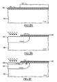
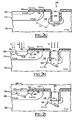
- Figs.2A-2J are sectional views of the N-channel DMOS transistor of Fig.1 at various stages of a fabrication process according to an embodiment of the present invention; and
- Fig.3 illustrates in sectional view a portion of an N-channel DMOS transistor according to another embodiment of the present invention, having a vertical source contact.
-
- With reference to Fig.1, a sectional view of a portion of an N-
channel DMOS transistor 100 according to an embodiment of the present invention is shown. The type of doping ions (acceptor and donor dopants) in the various regions of thetransistor 100 are indicated in the following, as usual in the art, by the letters P and N, respectively; the letters N and P have an added minus or plus sign to denote light or heavy doping ions concentrations. - The
DMOS transistor 100 is formed on an epitaxialmonocrystalline silicon layer 105, doped by N type dopants (N-epi) and grown on a silicon wafer substrate (not shown in the drawings); thetransistor 100 comprises adielectric layer 110 of silicon dioxide (SiO2), formed on the surface of theepitaxial layer 105, hereinafter referred to as thegate oxide 110. Over thegate oxide 110, aconductive gate layer 112 is provided, normally made of polysilicon. Thegate oxide 110 and thepolysilicon layer 112 define the gate region. Thegate oxide 110 separates two portions of an area on the epitaxial layer surface, which is intended to be an active area of thetransistor 100. - In one of the two portions of the active area a
P region 115, the so-called body region (P-body) of the transistor, is created, that extends under thegate oxide 110; a heavily Ndoped source region 120 is formed within thebody region 115. - The other portion of the active area includes a trench obtained in the
epitaxial layer 105, and a heavily Ndoped region 125 is provided at the bottom of the trench; theregion 125 constitutes the drain region of thetransistor 100. - A channel of N type carriers (i.e., electrons) for the transistor conduction current is formed during the transistor operation within a portion of the
body region 115 directly underlying thegate oxide 110, hereinafter referred to aschannel zone 130. Thedrain region 125 and thechannel zone 130 are separated by a portion identified by 135 of theepitaxial layer 105 underlying thegate oxide 110. - Insulating material (e.g., SiO2)
sidewall spacers 140 are formed adjacent to thegate oxide 110 extending from the surface of theconductive gate layer 112; in particular, aspacer 140 is formed along the trench vertical wall adjacent to the gate region and extends down to the trench bottom wall. - A lightly N doped (N-LDD)
region 145 is also provided in thebody region 115 and separates thesource region 120 and thechannel zone 130. Similarly, a further N-LDD region 150 is provided in theepitaxial layer 105 directly adjacent to thedrain region 125, and separates thedrain region 125 and theportion 135 of theepitaxial layer 105. Respective portions of the N-LDD regions adjacent spacer 140 and thegate oxide 110 for decreasing the voltage drop and, consequently, for reducing the oxide degradation at the gate oxide edge portions. - In the body region 115 a heavily P doped (P+)
region 155 is further provided adjacent to thesource region 120 on the opposite side with respect to the N-LDDregion 145, which is used to contact thebody region 115. - Contact windows are formed in an
insulating material layer 160 overlying the surface of thetransistor 100, andmetal contact plugs source region 120 and theP region 155, theconductive gate layer 112 and thedrain region 125 through respective contact windows for providing the source, gate and drain terminals S, G and D. In such a structure theP body region 115 and theN source region 120 are short-circuited and, consequently, they are both biased by the voltage provided to the source terminal S. - Preferably, for improving the characteristics of the contacts between metal and doped semiconductor regions,
silicide films source region 120 and theP region 155, and theN drain region 125, respectively. - By applying a suitable voltage to the gate terminal G of the
MOS transistor 100, the channel of electrons for the transistor conduction current forms within thechannel zone 130 directly underlying thegate oxide 110. When the drain and the source terminals D and S are properly biased, the conduction current flows towards thedrain region 125 at the bottom of the trench. Thanks to the position of thedrain region 125, lower than the position of thechannel zone 130 relative to the surface of thetransistor 100, the conduction current (indicated as I in the drawing) deviates deeply into theportion 135 of theepitaxial silicon layer 105, hereinafter referred to asdrift region 135, sufficiently far away from a gate oxide/silicon interface. - Consequently, the operation of the
transistor 100 is not or scarcely influenced by contaminations of the gate oxide or by imperfections of the walls of the trench; the gate oxide/silicon interface and the electrical properties of the transistor are substantially not degraded by the conduction current. Assuring high reliability, theDMOS transistor 100 withstands a relatively high voltage drop between the drain and the source terminals and a relatively great conduction current ranging from about 3 V to about 100 V and from about 100 mA to about 1 A, respectively, even if the transistor has a thin oxide layer. Furthermore, a transistor ON-resistance is relatively low and approximately of the order of mΩ/mm2; the parasitic capacitor between the gate and the drain terminals and the gate current are reduced. - In addition, the dimensions of the DMOS transistor can be very down-scaled, thanks to the fact that the conduction current flows transversely through the
drift region 135 exploiting a longer drift path than a conventional DMOS. - It is pointed out that the concepts of the present invention apply as well if the dopant types are inverted; both the N-
LDD regions region 145 or the region 150) can be formed. - The main stages of an exemplary process for the fabrication of the
transistor 100 according to an embodiment of the present invention are described hereinbelow with reference to Figs.2A-2J. - Referring to Fig.2A, the N layer of
monocrystalline silicon 105 is preferably formed by epitaxial growth at high temperature over the whole surface of the wafer substrate. Successively, a layer ofsilicon dioxide 205 is obtained at the surface of thesilicon layer 105, for example, by oxidation at high temperature of a superficial thickness of theepitaxial silicon layer 105 ranging from about 20 Å to about 400 Å. Over thesilicon dioxide layer 205, a conductivepolycristalline silicon layer 210 of thickness of about 1000 Å to about 5000 Å is deposited. - For defining the source region, firstly a
conventional mask 215 is exploited for a lithographic etching of the excess oxide andpolysilicon layers - As shown in Fig.2B, the
P region 115, intended to become the body region of the transistor, is formed into the portion of the active area uncovered by the first etching; preferably, an implant of P type dopants, for example boron ions, is performed. The implant may be executed in more steps, which differ for the implant doses and energies (ranging from 1·1013 cm-2 to 5·1013 cm-2 and from 50 keV to 100 keV, respectively). Preferably, the dopants are implanted along an angled implant direction such that theP body region 115 extends partially under theresidual oxide layer 205; in detail, thebody region 115 may have a depth ranging from 1·103 Å to 1·104 Å and a peak dopant concentration of about 1·1017-1·1018 cm-3. A high-energy implant of dopants is preferred over a thermal diffusion, because it allows keeping small the dimensions of thetransistor 100. - In a similar way, as illustrated in Fig.2C, donor ions, for example phosphorus or arsenic ions, are implanted into the
P body region 115 and made to diffuse towards the intendedchannel zone 130 under theresidual oxide layer 205, so as to form an lightly doped N region 220 (N-LDD). The implant dose and energy may, for example, be of about 1·1013-5·1013 cm-2 and 30-60 keV, respectively; in this way, theregion 220 has a peak donor concentration of about 1·1017-1·1018 cm-3. - Considering Fig.2D, a
second mask 225 is used for executing an anisotropic trench etching (for example, as described in US 6,093,588, which is incorporated herein by reference) into the portions of the oxide andpolysilicon layers epitaxial N layer 105 in the intended portion of the active area where the drain region has to be formed. - In this way, as shown in Fig.2E, a
trench 230 of a depth preferably ranging from 50 nm to 1 µm and a width ranging from 0.2 µm to 2 µm is obtained, extending roughly orthogonally to the wafer surface. At the end of this stage, thegate oxide 110 and thepolysilicon gate 112 forming the gate of the transistor are defined. - As depicted in Fig.2F, a further implant of N type dopants (e.g., As) is executed into the drain portion of the active area, at the bottom of the
trench 230, to form an drain lightly N doped (N-LDD)region 235. Also in this case, the implant may be executed in more steps and preferably with different implant angles, such that the drain N-LDD region 235 is also formed adjacent to the bottom portion of trenchvertical walls 233. The distance between the N-LDD region 235 and theP body region 115 defines a length Ld of thedrift region 135. - Referring to Fig.2G, the insulating
sidewall spacers 140 are then obtained, for example, by means of a selective thermal oxidation of the silicon or an oxide deposition and the etch-back thereof on the trenchvertical walls 233 and laterally to thegate oxide 110 and thepolysilicon gate 112. - As illustrated in Fig.2H, an implant of N type dopants (e.g., As) into the source and drain portion of the active area is performed for forming the source and drain
regions drain region 125 the implant is performed in a self-aligned way by thespacers 140 and thegate oxide 110; differently, a third mask (not shown) is used to selectively protect thebody region 115, thereby the dopants are implanted only in thesource region 120. In this way, also the two N-LDD regions 1014-1
- Successively, a fourth mask (not shown) is used to selectively implant P type dopants into the
P body region 115 for forming theP region 155 adjacent to theN source region 120 and used for properly contacting theP body region 115. - Then, a silicidation process is executed on the silicon wafer surface and the
films P regions N region 125, respectively. - As shown in Fig.2I, the
trench 230 is then filled, and the whole surface of the wafer is covered, with the insulatingmaterial layer 160, for example, silicon dioxide, preferably using a Chemical Vapor Deposition (shortly, CVD) process. - After this stage of the process, by means of a selective etching,
contact windows 245 are opened in the insulatingmaterial layer 160 over the P andN source regions N drain region 125 and over thepolysilicon gate 112, as shown in Fig.2J. - A
metal layer 250, for example aluminium, is then deposited, the metal filling also thecontact windows 245 for contacting theN source regions 120 and theP region 155, theN drain region 125 and thepolysilicon gate 112. - Finally, by means of a further selective etching the metal layer is properly patterned for forming the source, gate and drain
metal plugs transistor 100. - The above-described process can be used also for fabricating a plurality of transistors according to the present invention at the same time; expediently, two adjacent transistors are formed in such a way as to have the drain region or the source region in common. The process stages described above can be incorporated in a process for fabricating further different transistors or especially for fabricating (an) electronic circuit(s).
- However, the present invention can be applied also if the fabrication process of the transistor comprises additional stages or if the stages are executed in a different order and/or exploiting alternative techniques; particularly, the masks used during the process can be different in number and in type. Furthermore, alternative materials can be utilized for fabricating the device, such as different dopants, or different metals for the electric contacts, or different dielectrics.
- Fig.3 shows, in sectional view, a portion of an N-
channel DMOS transistor 100 according to another embodiment of the present invention, having a vertical source contact (the elements corresponding to those depicted in Fig.1 are denoted with the same reference numerals and their description is omitted for the sake of simplicity) . - In addition and similarly to the trench in correspondence of the drain region, a trench is etched also in the portion of the active area, where the source region has to be formed. A heavily doped N source region 320 (N+) is formed adjacent to the vertical wall of the source trench, while a heavily doped P region 355 (P+) is formed substantially at the bottom of the source trench. Alternatively, the
P region 355 may be formed adjacent to the vertical wall of the source trench opposite to thesource region 320, or partly at the bottom and partly along the vertical wall of the trench. - Preferably, to improve contact characteristics, a
silicide film 330 is formed on the vertical walls of the source trench and on the N-LDD region 145 and thesource region 320 in correspondence of the wafer surface. The trench at the source region is filled with metal, for obtaining a vertical sourcemetal contact plug 365s contacting theN source region 320 and theP region 355, similarly to thetransistor 100 described with reference to Fig.1. - Compared to the
transistor 100 of the first embodiment, the dimensions of theDMOS transistor 300 are further reduced thanks to the provision of the trench at the source region, which allows reducing of the width of thetransistor 300 by making possible a vertical contact 350 to thesource region 320, instead of a surface contact as in the embodiment of Fig.1. - It has to be observed that the
transistor 300 according to the second embodiment of the present invention can be realized preferably by etching simultaneously the intended source and drain portions in the active area in the fabrication process described with reference to Figs.2A-2J. Then, the N-type source and drainregions - Naturally, in order to satisfy specific requirements, a person skilled in the art may apply to the solution described above many modifications and alterations all of which, however, are included within the scope of protection of the invention as defined by the following claims.
Claims (26)
- An insulated-gate transistor (100;300), including:characterized in thata semiconductor material layer (105) having a front surface;a body region (115) of a first conductivity type formed in the semiconductor material layer in correspondence of the front surface;an insulated gate (112) insulatively disposed over the body region with interposition of a gate dielectric (110); anda source region (120,145;320,145) and a drain region (125,150) of a second conductivity type opposite to the first conductivity type, the source region being formed in the body region and the drain region being formed in the semiconductor material layer, the source and the drain regions being spaced apart from each other by:a channel zone (130) in a portion of the body region underlying the insulated gate, anda charge carriers drift portion (135) of the semiconductor material layer between the channel zone and the drain region, the insulated gate extending over the charge carriers drift portion,
the drain region is located at a depth compared to the front surface, for causing charge carriers to move in the charge carriers drift portion away from an interface between the semiconductor material layer and the gate dielectric. - The insulated-gate transistor according to claim 1, further including a trench (230) extending within the semiconductor material layer from the front surface, wherein the drain region is formed in correspondence of the trench.
- The insulated-gate transistor according to claim 2, wherein the drain region is formed substantially at a bottom of the trench.
- The insulated-gate transistor according to any of claims 2 or 3, further including a plurality dielectric material sidewall spacers (140) formed at edges of the insulated gate.
- The insulated-gate transistor according to claim 4, wherein the trench has a wall (233) adjacent to one edge of the insulated gate, the dielectric material sidewall spacer formed at said one edge extending aside said wall substantially to the bottom of the trench.
- The insulated-gate transistor according to any claim from 2 to 5, wherein the source region includes a first (120;320) and a second (145) source region portions, the second source region portion being adjacent to the channel zone and being less doped than the first source region portion.
- The insulated-gate transistor according to any claim from 2 to 6, wherein the drain region includes a first (125) and a second (150) drain region portions, the second drain region portion being adjacent to the drift region and being less doped than the first drain region portion.
- The insulated-gate transistor according to claim 7, wherein the second drain region portion partially extends along walls of the trench.
- The insulated-gate transistor according to any claim from 2 to 8, wherein the body region further includes a contact region (155;355) of the second conductivity type.
- The insulated-gate transistor according to any claim from 2 to 8, further including electrical contacts (170,165s,165g,175,165d;330,365s,165g,175,165d) to the source region, the body region, the gate dielectric and the drain region, respectively.
- The insulated-gate transistor according to claim 10, wherein the contact region and the source region are electrically connected to each other by a same electrical contact.
- The insulated-gate transistor according to any claim from 2 to 11, including a further trench, extending into the semiconductor layer from the front surface, wherein the source region is formed in correspondence of the further trench.
- The insulated-gate transistor according to claim 10, wherein the source region is adjacent to a wall of the further trench and the contact region is formed at a bottom of the further trench.
- An integrated circuit comprising at least one insulated-gate transistor according to any claim from 1 to 13.
- A process for fabricating an insulated-gate transistor (100;300), including the steps of:characterized in thatproviding a semiconductor material layer (105) having a front surface;forming a body region (115) of a first conductivity type in the semiconductor material layer in correspondence of the front surface;forming an insulated gate (112) insulatively disposed over the body region with interposition of a dielectric (110); andforming a source region (120,145;320,145) and a drain region (125,150) of a second conductivity type opposite to the first conductivity type, the source region being formed in the body region and the drain region being formed in the semiconductor material layer, the source and the drain region being spaced apart from each other by:a channel zone (130) in a portion of the body region underlying the insulated gate, anda charge carriers drift portion (135) of the semiconductor material layer between the channel zone and the drain region, the insulated gate extending over the charge carriers drift portion,
the drain region is formed at a depth compared to the front surface, for causing charge carriers to move in the charge carriers drift region away from an interface between the semiconductor material layer and the gate dielectric. - The process according to claim 15, further including forming a trench (230) extending within the semiconductor material layer from the front surface, and wherein said forming the drain region includes forming the drain region in correspondence of the trench, particularly substantially at a bottom of the trench.
- The process according to claim 16, wherein forming the trench includes performing a selective anisotropic etching of the semiconductor layer from the front surface.
- The process according to any claim from 16 to 17, wherein forming the body region includes:insulatively forming a gate conductive layer (210) over the front surface with interposition of a gate dielectric layer (205);selectively removing a portion of the gate dielectric and conductive layers from a portion of an intended device active area on the front surface; andoppositely doping the semiconductor layer in the active area portion to define the body region.
- The process according to any claim from 16 to 18, wherein forming the source and drain region includes
forming a first source and drain region portions (120,125;320,125), and
forming a second source and drain region portions (145,150) less doped than the first source and drain region portions, the second source region portion formed adjacent to the channel zone and the second drain region portion formed adjacent to the drift region. - The process according to claim 19, wherein forming the source and drain region further includes:oppositely doping a portion (220) of the body region;doping a portion (235) of the semiconductor material layer in correspondence of the trench; andselectively doping the portions of the body region and of the semiconductor material layer to define the first source and drain region portions more doped than the second source and drain region portions.
- The process according to claim 20, further including forming a contact region (155;355) of the second conductivity type in the portion of the body region, the contact region formed more doped than the body region.
- The process according to any claim from 16 to 21, further including forming a plurality dielectric material sidewall spacers (140) at edges of the insulated gate.
- The process according to claim 22, wherein forming the plurality dielectric material sidewall spacers includes forming a dielectric material sidewall spacer at one edge of the insulated gate adjacent to a wall (233) of the trench, the dielectric material sidewall spacer formed at said one edge of the insulated gate extending to the bottom of the trench.
- The process according to any claim from 16 to 23, further including forming electrical contacts (170,165s,165g,175,165d;330,365s,165g,175,165d) to the source region, the body region, the gate dielectric and the drain region, respectively.
- The process according to any claim from 21 to 24, further including forming a further trench, extending within the semiconductor material layer from the front surface, and wherein said forming the source region includes forming the source region in correspondence of the further trench, particularly adjacent to a wall of the further trench, and said forming the contact region includes forming the contact region at a bottom of the further trench.
- The process according to claim 25, wherein forming the further trench includes performing a further selective anisotropic etching of the semiconductor layer from the front surface.
Priority Applications (2)
| Application Number | Priority Date | Filing Date | Title |
|---|---|---|---|
| EP04100960.6A EP1577952B1 (en) | 2004-03-09 | 2004-03-09 | Method of making a high voltage insulated gate field-effect transistor |
| US11/078,909 US7417298B2 (en) | 2004-03-09 | 2005-03-09 | High voltage insulated-gate transistor |
Applications Claiming Priority (1)
| Application Number | Priority Date | Filing Date | Title |
|---|---|---|---|
| EP04100960.6A EP1577952B1 (en) | 2004-03-09 | 2004-03-09 | Method of making a high voltage insulated gate field-effect transistor |
Publications (2)
| Publication Number | Publication Date |
|---|---|
| EP1577952A1 true EP1577952A1 (en) | 2005-09-21 |
| EP1577952B1 EP1577952B1 (en) | 2018-07-04 |
Family
ID=34833751
Family Applications (1)
| Application Number | Title | Priority Date | Filing Date |
|---|---|---|---|
| EP04100960.6A Expired - Lifetime EP1577952B1 (en) | 2004-03-09 | 2004-03-09 | Method of making a high voltage insulated gate field-effect transistor |
Country Status (2)
| Country | Link |
|---|---|
| US (1) | US7417298B2 (en) |
| EP (1) | EP1577952B1 (en) |
Cited By (4)
| Publication number | Priority date | Publication date | Assignee | Title |
|---|---|---|---|---|
| TWI397154B (en) * | 2010-01-21 | 2013-05-21 | Great Power Semiconductor Corp | Trenched power semiconductor structure with schottky diode and fabrication method thereof |
| US9450076B2 (en) | 2014-01-21 | 2016-09-20 | Stmicroelectronics S.R.L. | Power LDMOS semiconductor device with reduced on-resistance and manufacturing method thereof |
| TWI624062B (en) * | 2014-06-17 | 2018-05-11 | 世界先進積體電路股份有限公司 | Method and apparatus for semiconductor device with reduced device footprint |
| CN114171585A (en) * | 2022-02-10 | 2022-03-11 | 北京芯可鉴科技有限公司 | LDMOSFET, preparation method, chip and circuit |
Families Citing this family (22)
| Publication number | Priority date | Publication date | Assignee | Title |
|---|---|---|---|---|
| KR100668856B1 (en) * | 2005-06-30 | 2007-01-16 | 주식회사 하이닉스반도체 | Manufacturing method of semiconductor device |
| US7868394B2 (en) * | 2005-08-09 | 2011-01-11 | United Microelectronics Corp. | Metal-oxide-semiconductor transistor and method of manufacturing the same |
| US7671411B2 (en) * | 2006-03-02 | 2010-03-02 | Volterra Semiconductor Corporation | Lateral double-diffused MOSFET transistor with a lightly doped source |
| JP4584222B2 (en) * | 2006-09-26 | 2010-11-17 | シャープ株式会社 | Manufacturing method of high voltage transistor |
| CN101542737B (en) * | 2006-11-16 | 2012-03-21 | Nxp股份有限公司 | Self-aligned impact-ionization field effect transistor |
| US7652329B2 (en) * | 2007-07-13 | 2010-01-26 | Semiconductor Components Industries, Llc | Vertical MOS transistor and method therefor |
| US7999318B2 (en) | 2007-12-28 | 2011-08-16 | Volterra Semiconductor Corporation | Heavily doped region in double-diffused source MOSFET (LDMOS) transistor and a method of fabricating the same |
| JP5272410B2 (en) * | 2008-01-11 | 2013-08-28 | 富士電機株式会社 | Semiconductor device and manufacturing method thereof |
| KR101057189B1 (en) * | 2008-11-12 | 2011-08-16 | 주식회사 하이닉스반도체 | Transistor for suppressing short channel effect and manufacturing method thereof |
| US8115253B2 (en) * | 2009-09-10 | 2012-02-14 | United Microelectronics Corp. | Ultra high voltage MOS transistor device |
| KR20110124584A (en) * | 2010-05-11 | 2011-11-17 | 삼성전자주식회사 | Semiconductor device having recess channel transistor and manufacturing method thereof |
| KR20120128979A (en) | 2011-05-18 | 2012-11-28 | 삼성전자주식회사 | Semiconductor Devices and Methods of Fabricating the Same |
| US9634135B2 (en) * | 2012-03-02 | 2017-04-25 | Microchip Technology Incorporated | Power field effect transistor |
| US9076837B2 (en) * | 2012-07-06 | 2015-07-07 | Taiwan Semiconductor Manufacturing Company, Ltd. | Lateral insulated gate bipolar transistor structure with low parasitic BJT gain and stable threshold voltage |
| US9324838B2 (en) | 2013-01-11 | 2016-04-26 | Stmicroelectronics S.R.L. | LDMOS power semiconductor device and manufacturing method of the same |
| EP3061124A4 (en) * | 2013-09-26 | 2017-04-26 | Intel Corporation | Vertical non-planar semiconductor device for system-on-chip (soc) applications |
| US20150145034A1 (en) * | 2013-11-24 | 2015-05-28 | United Microelectronics Corporation | Ldmos structure and manufacturing method thereof |
| JP6384315B2 (en) * | 2014-12-24 | 2018-09-05 | 富士通セミコンダクター株式会社 | Manufacturing method of semiconductor device |
| US9484431B1 (en) * | 2015-07-29 | 2016-11-01 | International Business Machines Corporation | Pure boron for silicide contact |
| TWI571939B (en) * | 2016-01-20 | 2017-02-21 | 力晶科技股份有限公司 | Laterally diffused metal oxide semiconductor device and method of manufacturing same |
| JP2019054106A (en) * | 2017-09-14 | 2019-04-04 | 株式会社東芝 | Semiconductor device |
| CN114242777A (en) * | 2022-02-22 | 2022-03-25 | 北京芯可鉴科技有限公司 | A kind of LDMOSFET, preparation method and chip and circuit |
Citations (6)
| Publication number | Priority date | Publication date | Assignee | Title |
|---|---|---|---|---|
| JPS5832462A (en) * | 1981-08-21 | 1983-02-25 | Toshiba Corp | Semiconductor device |
| EP0209949A2 (en) * | 1985-07-22 | 1987-01-28 | SILICONIX Incorporated | Method for forming a transistor, and transistor |
| US5701026A (en) * | 1994-10-25 | 1997-12-23 | Fuji Electric Co., Ltd. | Lateral trench MISFET |
| US6093588A (en) * | 1995-02-21 | 2000-07-25 | Stmicroelectronics, S.R.L. | Process for fabricating a high voltage MOSFET |
| US6252278B1 (en) * | 1998-05-18 | 2001-06-26 | Monolithic Power Systems, Inc. | Self-aligned lateral DMOS with spacer drift region |
| US6437399B1 (en) * | 1997-06-30 | 2002-08-20 | Fairchild Semiconductor Corporation | Semiconductor structures with trench contacts |
Family Cites Families (5)
| Publication number | Priority date | Publication date | Assignee | Title |
|---|---|---|---|---|
| US4983535A (en) | 1981-10-15 | 1991-01-08 | Siliconix Incorporated | Vertical DMOS transistor fabrication process |
| IT1254799B (en) | 1992-02-18 | 1995-10-11 | St Microelectronics Srl | VDMOS TRANSISTOR WITH IMPROVED VOLTAGE SEALING CHARACTERISTICS. |
| DE4300806C1 (en) | 1993-01-14 | 1993-12-23 | Siemens Ag | Vertical MOS transistor prodn. - with reduced trench spacing, without parasitic bipolar effects |
| US5356822A (en) | 1994-01-21 | 1994-10-18 | Alliedsignal Inc. | Method for making all complementary BiCDMOS devices |
| US6110799A (en) | 1997-06-30 | 2000-08-29 | Intersil Corporation | Trench contact process |
-
2004
- 2004-03-09 EP EP04100960.6A patent/EP1577952B1/en not_active Expired - Lifetime
-
2005
- 2005-03-09 US US11/078,909 patent/US7417298B2/en not_active Expired - Lifetime
Patent Citations (6)
| Publication number | Priority date | Publication date | Assignee | Title |
|---|---|---|---|---|
| JPS5832462A (en) * | 1981-08-21 | 1983-02-25 | Toshiba Corp | Semiconductor device |
| EP0209949A2 (en) * | 1985-07-22 | 1987-01-28 | SILICONIX Incorporated | Method for forming a transistor, and transistor |
| US5701026A (en) * | 1994-10-25 | 1997-12-23 | Fuji Electric Co., Ltd. | Lateral trench MISFET |
| US6093588A (en) * | 1995-02-21 | 2000-07-25 | Stmicroelectronics, S.R.L. | Process for fabricating a high voltage MOSFET |
| US6437399B1 (en) * | 1997-06-30 | 2002-08-20 | Fairchild Semiconductor Corporation | Semiconductor structures with trench contacts |
| US6252278B1 (en) * | 1998-05-18 | 2001-06-26 | Monolithic Power Systems, Inc. | Self-aligned lateral DMOS with spacer drift region |
Non-Patent Citations (1)
| Title |
|---|
| PATENT ABSTRACTS OF JAPAN vol. 0071, no. 11 (E - 175) 14 May 1983 (1983-05-14) * |
Cited By (6)
| Publication number | Priority date | Publication date | Assignee | Title |
|---|---|---|---|---|
| TWI397154B (en) * | 2010-01-21 | 2013-05-21 | Great Power Semiconductor Corp | Trenched power semiconductor structure with schottky diode and fabrication method thereof |
| US9450076B2 (en) | 2014-01-21 | 2016-09-20 | Stmicroelectronics S.R.L. | Power LDMOS semiconductor device with reduced on-resistance and manufacturing method thereof |
| US9484436B2 (en) | 2014-01-21 | 2016-11-01 | Stmicroelectronics S.R.L. | Power LDMOS semiconductor device with reduced on-resistance and manufacturing method thereof |
| TWI624062B (en) * | 2014-06-17 | 2018-05-11 | 世界先進積體電路股份有限公司 | Method and apparatus for semiconductor device with reduced device footprint |
| CN114171585A (en) * | 2022-02-10 | 2022-03-11 | 北京芯可鉴科技有限公司 | LDMOSFET, preparation method, chip and circuit |
| CN114171585B (en) * | 2022-02-10 | 2022-05-17 | 北京芯可鉴科技有限公司 | A kind of LDMOSFET, preparation method and chip and circuit |
Also Published As
| Publication number | Publication date |
|---|---|
| US7417298B2 (en) | 2008-08-26 |
| EP1577952B1 (en) | 2018-07-04 |
| US20050205897A1 (en) | 2005-09-22 |
Similar Documents
| Publication | Publication Date | Title |
|---|---|---|
| US7417298B2 (en) | High voltage insulated-gate transistor | |
| JP2932429B2 (en) | MOS field effect transistor and method of manufacturing the same | |
| US8021947B2 (en) | Method of forming an insulated gate field effect transistor device having a shield electrode structure | |
| US7602037B2 (en) | High voltage semiconductor devices and methods for fabricating the same | |
| US7851312B2 (en) | Semiconductor component and method of manufacture | |
| US7821063B2 (en) | Semiconductor device having enhanced performance and method | |
| US20110012174A1 (en) | Structure and Method for Forming Field Effect Transistor with Low Resistance Channel Region | |
| KR101332590B1 (en) | Power semiconductor device having improved performance and method | |
| US20070267672A1 (en) | Semiconductor device and method for manufacturing same | |
| US7768078B2 (en) | Power semiconductor device having improved performance and method | |
| US20080038891A1 (en) | HIGH VOLTAGE MOSFET HAVING Si/SiGe HETEROJUNCTION STRUCTURE AND METHOD OF MANUFACTURING THE SAME | |
| US6888176B1 (en) | Thyrister semiconductor device | |
| US6777745B2 (en) | Symmetric trench MOSFET device and method of making same | |
| JPH11238877A (en) | Vertical MISFET and manufacturing method thereof | |
| US12230709B2 (en) | Transistor structure and manufacturing method of the same | |
| EP0964454A1 (en) | Field-effect transistor having a lightly doped drain region and method of making the same | |
| KR20000051294A (en) | DMOS field effect transistor with improved electrical characteristics and fabricating method thereof | |
| US7279367B1 (en) | Method of manufacturing a thyristor semiconductor device | |
| US7119435B2 (en) | Semiconductor device with source/drain extension layer | |
| US20050139858A1 (en) | Lateral double-diffused MOS transistor device | |
| US10553714B2 (en) | Method for fabricating a folded channel trench MOSFET |
Legal Events
| Date | Code | Title | Description |
|---|---|---|---|
| PUAI | Public reference made under article 153(3) epc to a published international application that has entered the european phase |
Free format text: ORIGINAL CODE: 0009012 |
|
| AK | Designated contracting states |
Kind code of ref document: A1 Designated state(s): AT BE BG CH CY CZ DE DK EE ES FI FR GB GR HU IE IT LI LU MC NL PL PT RO SE SI SK TR |
|
| AX | Request for extension of the european patent |
Extension state: AL LT LV MK |
|
| 17P | Request for examination filed |
Effective date: 20050921 |
|
| AKX | Designation fees paid |
Designated state(s): DE FR GB IT |
|
| 17Q | First examination report despatched |
Effective date: 20090320 |
|
| RAP1 | Party data changed (applicant data changed or rights of an application transferred) |
Owner name: STMICROELECTRONICS SRL |
|
| RAP1 | Party data changed (applicant data changed or rights of an application transferred) |
Owner name: STMICROELECTRONICS SRL |
|
| GRAP | Despatch of communication of intention to grant a patent |
Free format text: ORIGINAL CODE: EPIDOSNIGR1 |
|
| INTG | Intention to grant announced |
Effective date: 20180129 |
|
| RIN1 | Information on inventor provided before grant (corrected) |
Inventor name: DEPETRO, RICCARDO Inventor name: MANZINI, STEFANO |
|
| GRAS | Grant fee paid |
Free format text: ORIGINAL CODE: EPIDOSNIGR3 |
|
| GRAA | (expected) grant |
Free format text: ORIGINAL CODE: 0009210 |
|
| AK | Designated contracting states |
Kind code of ref document: B1 Designated state(s): DE FR GB IT |
|
| REG | Reference to a national code |
Ref country code: GB Ref legal event code: FG4D |
|
| REG | Reference to a national code |
Ref country code: DE Ref legal event code: R096 Ref document number: 602004052886 Country of ref document: DE |
|
| RIC2 | Information provided on ipc code assigned after grant |
Ipc: H01L 29/08 20060101ALI20040811BHEP Ipc: H01L 21/336 20060101ALI20040811BHEP Ipc: H01L 29/417 20060101ALI20040811BHEP Ipc: H01L 29/78 20060101AFI20040811BHEP |
|
| REG | Reference to a national code |
Ref country code: DE Ref legal event code: R097 Ref document number: 602004052886 Country of ref document: DE |
|
| PG25 | Lapsed in a contracting state [announced via postgrant information from national office to epo] |
Ref country code: IT Free format text: LAPSE BECAUSE OF FAILURE TO SUBMIT A TRANSLATION OF THE DESCRIPTION OR TO PAY THE FEE WITHIN THE PRESCRIBED TIME-LIMIT Effective date: 20180704 |
|
| PLBE | No opposition filed within time limit |
Free format text: ORIGINAL CODE: 0009261 |
|
| STAA | Information on the status of an ep patent application or granted ep patent |
Free format text: STATUS: NO OPPOSITION FILED WITHIN TIME LIMIT |
|
| 26N | No opposition filed |
Effective date: 20190405 |
|
| GBPC | Gb: european patent ceased through non-payment of renewal fee |
Effective date: 20190309 |
|
| PG25 | Lapsed in a contracting state [announced via postgrant information from national office to epo] |
Ref country code: GB Free format text: LAPSE BECAUSE OF NON-PAYMENT OF DUE FEES Effective date: 20190309 |
|
| PG25 | Lapsed in a contracting state [announced via postgrant information from national office to epo] |
Ref country code: FR Free format text: LAPSE BECAUSE OF NON-PAYMENT OF DUE FEES Effective date: 20190331 |
|
| PGFP | Annual fee paid to national office [announced via postgrant information from national office to epo] |
Ref country code: DE Payment date: 20230221 Year of fee payment: 20 |
|
| REG | Reference to a national code |
Ref country code: DE Ref legal event code: R071 Ref document number: 602004052886 Country of ref document: DE |