EP1577888A2 - Optical recording medium - Google Patents
Optical recording medium Download PDFInfo
- Publication number
- EP1577888A2 EP1577888A2 EP03746893A EP03746893A EP1577888A2 EP 1577888 A2 EP1577888 A2 EP 1577888A2 EP 03746893 A EP03746893 A EP 03746893A EP 03746893 A EP03746893 A EP 03746893A EP 1577888 A2 EP1577888 A2 EP 1577888A2
- Authority
- EP
- European Patent Office
- Prior art keywords
- layer
- optical recording
- recording
- recording medium
- dielectric layer
- Prior art date
- Legal status (The legal status is an assumption and is not a legal conclusion. Google has not performed a legal analysis and makes no representation as to the accuracy of the status listed.)
- Withdrawn
Links
Images


Classifications
-
- G—PHYSICS
- G11—INFORMATION STORAGE
- G11B—INFORMATION STORAGE BASED ON RELATIVE MOVEMENT BETWEEN RECORD CARRIER AND TRANSDUCER
- G11B7/00—Recording or reproducing by optical means, e.g. recording using a thermal beam of optical radiation by modifying optical properties or the physical structure, reproducing using an optical beam at lower power by sensing optical properties; Record carriers therefor
- G11B7/24—Record carriers characterised by shape, structure or physical properties, or by the selection of the material
- G11B7/2403—Layers; Shape, structure or physical properties thereof
- G11B7/24067—Combinations of two or more layers with specific interrelation
-
- G—PHYSICS
- G11—INFORMATION STORAGE
- G11B—INFORMATION STORAGE BASED ON RELATIVE MOVEMENT BETWEEN RECORD CARRIER AND TRANSDUCER
- G11B7/00—Recording or reproducing by optical means, e.g. recording using a thermal beam of optical radiation by modifying optical properties or the physical structure, reproducing using an optical beam at lower power by sensing optical properties; Record carriers therefor
- G11B7/24—Record carriers characterised by shape, structure or physical properties, or by the selection of the material
- G11B7/241—Record carriers characterised by shape, structure or physical properties, or by the selection of the material characterised by the selection of the material
- G11B7/242—Record carriers characterised by shape, structure or physical properties, or by the selection of the material characterised by the selection of the material of recording layers
- G11B7/243—Record carriers characterised by shape, structure or physical properties, or by the selection of the material characterised by the selection of the material of recording layers comprising inorganic materials only, e.g. ablative layers
- G11B7/2433—Metals or elements of groups 13, 14, 15 or 16 of the Periodic System, e.g. B, Si, Ge, As, Sb, Bi, Se or Te
-
- G—PHYSICS
- G11—INFORMATION STORAGE
- G11B—INFORMATION STORAGE BASED ON RELATIVE MOVEMENT BETWEEN RECORD CARRIER AND TRANSDUCER
- G11B7/00—Recording or reproducing by optical means, e.g. recording using a thermal beam of optical radiation by modifying optical properties or the physical structure, reproducing using an optical beam at lower power by sensing optical properties; Record carriers therefor
- G11B7/24—Record carriers characterised by shape, structure or physical properties, or by the selection of the material
- G11B7/241—Record carriers characterised by shape, structure or physical properties, or by the selection of the material characterised by the selection of the material
- G11B7/252—Record carriers characterised by shape, structure or physical properties, or by the selection of the material characterised by the selection of the material of layers other than recording layers
- G11B7/257—Record carriers characterised by shape, structure or physical properties, or by the selection of the material characterised by the selection of the material of layers other than recording layers of layers having properties involved in recording or reproduction, e.g. optical interference layers or sensitising layers or dielectric layers, which are protecting the recording layers
- G11B7/2578—Record carriers characterised by shape, structure or physical properties, or by the selection of the material characterised by the selection of the material of layers other than recording layers of layers having properties involved in recording or reproduction, e.g. optical interference layers or sensitising layers or dielectric layers, which are protecting the recording layers consisting essentially of inorganic materials
-
- G—PHYSICS
- G11—INFORMATION STORAGE
- G11B—INFORMATION STORAGE BASED ON RELATIVE MOVEMENT BETWEEN RECORD CARRIER AND TRANSDUCER
- G11B7/00—Recording or reproducing by optical means, e.g. recording using a thermal beam of optical radiation by modifying optical properties or the physical structure, reproducing using an optical beam at lower power by sensing optical properties; Record carriers therefor
- G11B7/24—Record carriers characterised by shape, structure or physical properties, or by the selection of the material
- G11B7/241—Record carriers characterised by shape, structure or physical properties, or by the selection of the material characterised by the selection of the material
- G11B7/242—Record carriers characterised by shape, structure or physical properties, or by the selection of the material characterised by the selection of the material of recording layers
- G11B7/243—Record carriers characterised by shape, structure or physical properties, or by the selection of the material characterised by the selection of the material of recording layers comprising inorganic materials only, e.g. ablative layers
- G11B2007/24302—Metals or metalloids
- G11B2007/2431—Metals or metalloids group 13 elements (B, Al, Ga, In)
-
- G—PHYSICS
- G11—INFORMATION STORAGE
- G11B—INFORMATION STORAGE BASED ON RELATIVE MOVEMENT BETWEEN RECORD CARRIER AND TRANSDUCER
- G11B7/00—Recording or reproducing by optical means, e.g. recording using a thermal beam of optical radiation by modifying optical properties or the physical structure, reproducing using an optical beam at lower power by sensing optical properties; Record carriers therefor
- G11B7/24—Record carriers characterised by shape, structure or physical properties, or by the selection of the material
- G11B7/241—Record carriers characterised by shape, structure or physical properties, or by the selection of the material characterised by the selection of the material
- G11B7/242—Record carriers characterised by shape, structure or physical properties, or by the selection of the material characterised by the selection of the material of recording layers
- G11B7/243—Record carriers characterised by shape, structure or physical properties, or by the selection of the material characterised by the selection of the material of recording layers comprising inorganic materials only, e.g. ablative layers
- G11B2007/24302—Metals or metalloids
- G11B2007/24312—Metals or metalloids group 14 elements (e.g. Si, Ge, Sn)
-
- G—PHYSICS
- G11—INFORMATION STORAGE
- G11B—INFORMATION STORAGE BASED ON RELATIVE MOVEMENT BETWEEN RECORD CARRIER AND TRANSDUCER
- G11B7/00—Recording or reproducing by optical means, e.g. recording using a thermal beam of optical radiation by modifying optical properties or the physical structure, reproducing using an optical beam at lower power by sensing optical properties; Record carriers therefor
- G11B7/24—Record carriers characterised by shape, structure or physical properties, or by the selection of the material
- G11B7/241—Record carriers characterised by shape, structure or physical properties, or by the selection of the material characterised by the selection of the material
- G11B7/242—Record carriers characterised by shape, structure or physical properties, or by the selection of the material characterised by the selection of the material of recording layers
- G11B7/243—Record carriers characterised by shape, structure or physical properties, or by the selection of the material characterised by the selection of the material of recording layers comprising inorganic materials only, e.g. ablative layers
- G11B2007/24302—Metals or metalloids
- G11B2007/24314—Metals or metalloids group 15 elements (e.g. Sb, Bi)
-
- G—PHYSICS
- G11—INFORMATION STORAGE
- G11B—INFORMATION STORAGE BASED ON RELATIVE MOVEMENT BETWEEN RECORD CARRIER AND TRANSDUCER
- G11B7/00—Recording or reproducing by optical means, e.g. recording using a thermal beam of optical radiation by modifying optical properties or the physical structure, reproducing using an optical beam at lower power by sensing optical properties; Record carriers therefor
- G11B7/24—Record carriers characterised by shape, structure or physical properties, or by the selection of the material
- G11B7/241—Record carriers characterised by shape, structure or physical properties, or by the selection of the material characterised by the selection of the material
- G11B7/242—Record carriers characterised by shape, structure or physical properties, or by the selection of the material characterised by the selection of the material of recording layers
- G11B7/243—Record carriers characterised by shape, structure or physical properties, or by the selection of the material characterised by the selection of the material of recording layers comprising inorganic materials only, e.g. ablative layers
- G11B2007/24302—Metals or metalloids
- G11B2007/24316—Metals or metalloids group 16 elements (i.e. chalcogenides, Se, Te)
-
- G—PHYSICS
- G11—INFORMATION STORAGE
- G11B—INFORMATION STORAGE BASED ON RELATIVE MOVEMENT BETWEEN RECORD CARRIER AND TRANSDUCER
- G11B7/00—Recording or reproducing by optical means, e.g. recording using a thermal beam of optical radiation by modifying optical properties or the physical structure, reproducing using an optical beam at lower power by sensing optical properties; Record carriers therefor
- G11B7/24—Record carriers characterised by shape, structure or physical properties, or by the selection of the material
- G11B7/241—Record carriers characterised by shape, structure or physical properties, or by the selection of the material characterised by the selection of the material
- G11B7/252—Record carriers characterised by shape, structure or physical properties, or by the selection of the material characterised by the selection of the material of layers other than recording layers
- G11B7/257—Record carriers characterised by shape, structure or physical properties, or by the selection of the material characterised by the selection of the material of layers other than recording layers of layers having properties involved in recording or reproduction, e.g. optical interference layers or sensitising layers or dielectric layers, which are protecting the recording layers
- G11B2007/25705—Record carriers characterised by shape, structure or physical properties, or by the selection of the material characterised by the selection of the material of layers other than recording layers of layers having properties involved in recording or reproduction, e.g. optical interference layers or sensitising layers or dielectric layers, which are protecting the recording layers consisting essentially of inorganic materials
- G11B2007/25706—Record carriers characterised by shape, structure or physical properties, or by the selection of the material characterised by the selection of the material of layers other than recording layers of layers having properties involved in recording or reproduction, e.g. optical interference layers or sensitising layers or dielectric layers, which are protecting the recording layers consisting essentially of inorganic materials containing transition metal elements (Zn, Fe, Co, Ni, Pt)
-
- G—PHYSICS
- G11—INFORMATION STORAGE
- G11B—INFORMATION STORAGE BASED ON RELATIVE MOVEMENT BETWEEN RECORD CARRIER AND TRANSDUCER
- G11B7/00—Recording or reproducing by optical means, e.g. recording using a thermal beam of optical radiation by modifying optical properties or the physical structure, reproducing using an optical beam at lower power by sensing optical properties; Record carriers therefor
- G11B7/24—Record carriers characterised by shape, structure or physical properties, or by the selection of the material
- G11B7/241—Record carriers characterised by shape, structure or physical properties, or by the selection of the material characterised by the selection of the material
- G11B7/252—Record carriers characterised by shape, structure or physical properties, or by the selection of the material characterised by the selection of the material of layers other than recording layers
- G11B7/257—Record carriers characterised by shape, structure or physical properties, or by the selection of the material characterised by the selection of the material of layers other than recording layers of layers having properties involved in recording or reproduction, e.g. optical interference layers or sensitising layers or dielectric layers, which are protecting the recording layers
- G11B2007/25705—Record carriers characterised by shape, structure or physical properties, or by the selection of the material characterised by the selection of the material of layers other than recording layers of layers having properties involved in recording or reproduction, e.g. optical interference layers or sensitising layers or dielectric layers, which are protecting the recording layers consisting essentially of inorganic materials
- G11B2007/25708—Record carriers characterised by shape, structure or physical properties, or by the selection of the material characterised by the selection of the material of layers other than recording layers of layers having properties involved in recording or reproduction, e.g. optical interference layers or sensitising layers or dielectric layers, which are protecting the recording layers consisting essentially of inorganic materials containing group 13 elements (B, Al, Ga)
-
- G—PHYSICS
- G11—INFORMATION STORAGE
- G11B—INFORMATION STORAGE BASED ON RELATIVE MOVEMENT BETWEEN RECORD CARRIER AND TRANSDUCER
- G11B7/00—Recording or reproducing by optical means, e.g. recording using a thermal beam of optical radiation by modifying optical properties or the physical structure, reproducing using an optical beam at lower power by sensing optical properties; Record carriers therefor
- G11B7/24—Record carriers characterised by shape, structure or physical properties, or by the selection of the material
- G11B7/241—Record carriers characterised by shape, structure or physical properties, or by the selection of the material characterised by the selection of the material
- G11B7/252—Record carriers characterised by shape, structure or physical properties, or by the selection of the material characterised by the selection of the material of layers other than recording layers
- G11B7/257—Record carriers characterised by shape, structure or physical properties, or by the selection of the material characterised by the selection of the material of layers other than recording layers of layers having properties involved in recording or reproduction, e.g. optical interference layers or sensitising layers or dielectric layers, which are protecting the recording layers
- G11B2007/25705—Record carriers characterised by shape, structure or physical properties, or by the selection of the material characterised by the selection of the material of layers other than recording layers of layers having properties involved in recording or reproduction, e.g. optical interference layers or sensitising layers or dielectric layers, which are protecting the recording layers consisting essentially of inorganic materials
- G11B2007/2571—Record carriers characterised by shape, structure or physical properties, or by the selection of the material characterised by the selection of the material of layers other than recording layers of layers having properties involved in recording or reproduction, e.g. optical interference layers or sensitising layers or dielectric layers, which are protecting the recording layers consisting essentially of inorganic materials containing group 14 elements except carbon (Si, Ge, Sn, Pb)
-
- G—PHYSICS
- G11—INFORMATION STORAGE
- G11B—INFORMATION STORAGE BASED ON RELATIVE MOVEMENT BETWEEN RECORD CARRIER AND TRANSDUCER
- G11B7/00—Recording or reproducing by optical means, e.g. recording using a thermal beam of optical radiation by modifying optical properties or the physical structure, reproducing using an optical beam at lower power by sensing optical properties; Record carriers therefor
- G11B7/24—Record carriers characterised by shape, structure or physical properties, or by the selection of the material
- G11B7/241—Record carriers characterised by shape, structure or physical properties, or by the selection of the material characterised by the selection of the material
- G11B7/252—Record carriers characterised by shape, structure or physical properties, or by the selection of the material characterised by the selection of the material of layers other than recording layers
- G11B7/257—Record carriers characterised by shape, structure or physical properties, or by the selection of the material characterised by the selection of the material of layers other than recording layers of layers having properties involved in recording or reproduction, e.g. optical interference layers or sensitising layers or dielectric layers, which are protecting the recording layers
- G11B2007/25705—Record carriers characterised by shape, structure or physical properties, or by the selection of the material characterised by the selection of the material of layers other than recording layers of layers having properties involved in recording or reproduction, e.g. optical interference layers or sensitising layers or dielectric layers, which are protecting the recording layers consisting essentially of inorganic materials
- G11B2007/25713—Record carriers characterised by shape, structure or physical properties, or by the selection of the material characterised by the selection of the material of layers other than recording layers of layers having properties involved in recording or reproduction, e.g. optical interference layers or sensitising layers or dielectric layers, which are protecting the recording layers consisting essentially of inorganic materials containing nitrogen
-
- G—PHYSICS
- G11—INFORMATION STORAGE
- G11B—INFORMATION STORAGE BASED ON RELATIVE MOVEMENT BETWEEN RECORD CARRIER AND TRANSDUCER
- G11B7/00—Recording or reproducing by optical means, e.g. recording using a thermal beam of optical radiation by modifying optical properties or the physical structure, reproducing using an optical beam at lower power by sensing optical properties; Record carriers therefor
- G11B7/24—Record carriers characterised by shape, structure or physical properties, or by the selection of the material
- G11B7/241—Record carriers characterised by shape, structure or physical properties, or by the selection of the material characterised by the selection of the material
- G11B7/252—Record carriers characterised by shape, structure or physical properties, or by the selection of the material characterised by the selection of the material of layers other than recording layers
- G11B7/257—Record carriers characterised by shape, structure or physical properties, or by the selection of the material characterised by the selection of the material of layers other than recording layers of layers having properties involved in recording or reproduction, e.g. optical interference layers or sensitising layers or dielectric layers, which are protecting the recording layers
- G11B2007/25705—Record carriers characterised by shape, structure or physical properties, or by the selection of the material characterised by the selection of the material of layers other than recording layers of layers having properties involved in recording or reproduction, e.g. optical interference layers or sensitising layers or dielectric layers, which are protecting the recording layers consisting essentially of inorganic materials
- G11B2007/25715—Record carriers characterised by shape, structure or physical properties, or by the selection of the material characterised by the selection of the material of layers other than recording layers of layers having properties involved in recording or reproduction, e.g. optical interference layers or sensitising layers or dielectric layers, which are protecting the recording layers consisting essentially of inorganic materials containing oxygen
-
- G—PHYSICS
- G11—INFORMATION STORAGE
- G11B—INFORMATION STORAGE BASED ON RELATIVE MOVEMENT BETWEEN RECORD CARRIER AND TRANSDUCER
- G11B7/00—Recording or reproducing by optical means, e.g. recording using a thermal beam of optical radiation by modifying optical properties or the physical structure, reproducing using an optical beam at lower power by sensing optical properties; Record carriers therefor
- G11B7/24—Record carriers characterised by shape, structure or physical properties, or by the selection of the material
- G11B7/241—Record carriers characterised by shape, structure or physical properties, or by the selection of the material characterised by the selection of the material
- G11B7/252—Record carriers characterised by shape, structure or physical properties, or by the selection of the material characterised by the selection of the material of layers other than recording layers
- G11B7/257—Record carriers characterised by shape, structure or physical properties, or by the selection of the material characterised by the selection of the material of layers other than recording layers of layers having properties involved in recording or reproduction, e.g. optical interference layers or sensitising layers or dielectric layers, which are protecting the recording layers
- G11B2007/25705—Record carriers characterised by shape, structure or physical properties, or by the selection of the material characterised by the selection of the material of layers other than recording layers of layers having properties involved in recording or reproduction, e.g. optical interference layers or sensitising layers or dielectric layers, which are protecting the recording layers consisting essentially of inorganic materials
- G11B2007/25716—Record carriers characterised by shape, structure or physical properties, or by the selection of the material characterised by the selection of the material of layers other than recording layers of layers having properties involved in recording or reproduction, e.g. optical interference layers or sensitising layers or dielectric layers, which are protecting the recording layers consisting essentially of inorganic materials containing sulfur
-
- G—PHYSICS
- G11—INFORMATION STORAGE
- G11B—INFORMATION STORAGE BASED ON RELATIVE MOVEMENT BETWEEN RECORD CARRIER AND TRANSDUCER
- G11B7/00—Recording or reproducing by optical means, e.g. recording using a thermal beam of optical radiation by modifying optical properties or the physical structure, reproducing using an optical beam at lower power by sensing optical properties; Record carriers therefor
- G11B7/24—Record carriers characterised by shape, structure or physical properties, or by the selection of the material
- G11B7/241—Record carriers characterised by shape, structure or physical properties, or by the selection of the material characterised by the selection of the material
- G11B7/252—Record carriers characterised by shape, structure or physical properties, or by the selection of the material characterised by the selection of the material of layers other than recording layers
- G11B7/253—Record carriers characterised by shape, structure or physical properties, or by the selection of the material characterised by the selection of the material of layers other than recording layers of substrates
- G11B7/2531—Record carriers characterised by shape, structure or physical properties, or by the selection of the material characterised by the selection of the material of layers other than recording layers of substrates comprising glass
-
- G—PHYSICS
- G11—INFORMATION STORAGE
- G11B—INFORMATION STORAGE BASED ON RELATIVE MOVEMENT BETWEEN RECORD CARRIER AND TRANSDUCER
- G11B7/00—Recording or reproducing by optical means, e.g. recording using a thermal beam of optical radiation by modifying optical properties or the physical structure, reproducing using an optical beam at lower power by sensing optical properties; Record carriers therefor
- G11B7/24—Record carriers characterised by shape, structure or physical properties, or by the selection of the material
- G11B7/241—Record carriers characterised by shape, structure or physical properties, or by the selection of the material characterised by the selection of the material
- G11B7/252—Record carriers characterised by shape, structure or physical properties, or by the selection of the material characterised by the selection of the material of layers other than recording layers
- G11B7/253—Record carriers characterised by shape, structure or physical properties, or by the selection of the material characterised by the selection of the material of layers other than recording layers of substrates
- G11B7/2533—Record carriers characterised by shape, structure or physical properties, or by the selection of the material characterised by the selection of the material of layers other than recording layers of substrates comprising resins
- G11B7/2534—Record carriers characterised by shape, structure or physical properties, or by the selection of the material characterised by the selection of the material of layers other than recording layers of substrates comprising resins polycarbonates [PC]
-
- G—PHYSICS
- G11—INFORMATION STORAGE
- G11B—INFORMATION STORAGE BASED ON RELATIVE MOVEMENT BETWEEN RECORD CARRIER AND TRANSDUCER
- G11B7/00—Recording or reproducing by optical means, e.g. recording using a thermal beam of optical radiation by modifying optical properties or the physical structure, reproducing using an optical beam at lower power by sensing optical properties; Record carriers therefor
- G11B7/24—Record carriers characterised by shape, structure or physical properties, or by the selection of the material
- G11B7/241—Record carriers characterised by shape, structure or physical properties, or by the selection of the material characterised by the selection of the material
- G11B7/252—Record carriers characterised by shape, structure or physical properties, or by the selection of the material characterised by the selection of the material of layers other than recording layers
- G11B7/254—Record carriers characterised by shape, structure or physical properties, or by the selection of the material characterised by the selection of the material of layers other than recording layers of protective topcoat layers
- G11B7/2542—Record carriers characterised by shape, structure or physical properties, or by the selection of the material characterised by the selection of the material of layers other than recording layers of protective topcoat layers consisting essentially of organic resins
-
- G—PHYSICS
- G11—INFORMATION STORAGE
- G11B—INFORMATION STORAGE BASED ON RELATIVE MOVEMENT BETWEEN RECORD CARRIER AND TRANSDUCER
- G11B7/00—Recording or reproducing by optical means, e.g. recording using a thermal beam of optical radiation by modifying optical properties or the physical structure, reproducing using an optical beam at lower power by sensing optical properties; Record carriers therefor
- G11B7/24—Record carriers characterised by shape, structure or physical properties, or by the selection of the material
- G11B7/241—Record carriers characterised by shape, structure or physical properties, or by the selection of the material characterised by the selection of the material
- G11B7/252—Record carriers characterised by shape, structure or physical properties, or by the selection of the material characterised by the selection of the material of layers other than recording layers
- G11B7/258—Record carriers characterised by shape, structure or physical properties, or by the selection of the material characterised by the selection of the material of layers other than recording layers of reflective layers
- G11B7/259—Record carriers characterised by shape, structure or physical properties, or by the selection of the material characterised by the selection of the material of layers other than recording layers of reflective layers based on silver
Definitions
- the present invention relates to an optical recording medium constructed so that the recording or reproduction of information can be carried out by irradiation with recording light or reproduction light.
- Optical recording media that are capable of high-density recording and on which recorded information can be deleted and overwritten (hereinafter referred to as "rewritable optical recording media”) have been subject to much attention in recent years.
- Information is recorded on phase-change optical recording media, which are one example of such rewritable optical recording media, by changing the crystal state of a recording layer through irradiation with laser light. Recorded information is reproduced by detecting changes in the reflectivity of the recording layer due to such changes in the crystal state.
- Phase-change optical recording media have been subject to particular attention since it is possible to record and reproduce information using an optical system with a simpler construction than an optical system used with magneto-optical recording media.
- chalcogenide compounds such as Ge-Sb-Te materials
- Ge-Sb-Te materials are normally used as the optical material of the recording layer for reasons such as the large difference in the reflectivity between the crystal state and the amorphous state and also the relatively high stability of suchmaterials in the amorphous state.
- the recording layer is irradiated by laser light (a recording laser beam) set at a high power (the "recording power") capable of raising the temperature of the recording layer to the melting point or above.
- the recording power a high power
- amorphous recording marks are formed at the positions that were irradiated by the laser light of the recording power through rapid cooling after the recording layer has melted.
- the marks are irradiated by laser light of relatively low power (the “erasing power”) that is capable of raising the temperature of the recording layer to the crystallization temperature or above but below the melting point.
- the parts that were irradiated by the laser light of the erasing power are slowly cooled after the recording layer has been heated to the crystallization temperature or above, so that the recording marks (amorphous parts) are restored to the crystal state (i.e., the recording marks are erased) .
- the power (irradiating power) of a single laser beam it is possible to overwrite the recording data on a rewritable phase-change optical recording medium.
- the spot diameter of the recording laser beam emitted onto the surface of the recording layer is expressed as ⁇ /NA where ⁇ is the wavelength of the laser light and NA is the numerical aperture of the objective lens, and as this value ⁇ /NA becomes smaller, it becomes possible to record and reproduce smaller recording marks and also possible to carry out recording and reproduction of an optical recording medium with a narrower track pitch.
- the present inventors discovered the following problems. That is, with a conventional optical recording medium, to make the overwriting of recorded data possible, the recording layer is constructed so that amorphous parts (recording marks) can be restored to the crystalline state (i.e., the recording marks can be erased) by irradiation with laser light of the erasing power. For this reason, to prevent recording marks from being erased by a reproduction laser beam emitted during the reproduction of recorded information on this kind of optical recording medium, a low power laser light that does not affect the crystalline state of the recording marks is normally used.
- the present invention was conceived in order to solve the problems described above, and it is a principal object of the present invention to provide an optical recording medium that can be recorded at high density and can also improve the reproduction durability and reduce cross-erasing.
- An optical recording medium includes a recording layer, a first absorbing layer and a heat sink layer formed in order from an incident side for light used for recording or light used for reproduction, the first absorbing layer having an extinction coefficient k for a wavelength of the light used for recording or the light used for reproduction that satisfies 0.06 ⁇ k ⁇ 1.0.
- this optical recording medium by constructing the first absorbing layer so that the extinction coefficient k for the wavelength of the light used for recording or for reproduction satisfies 0.06 ⁇ k ⁇ 1.0, it is possible to sufficiently improve the reproduction durability and to sufficiently reduce cross-erasing, even when recording at high density.
- the optical recording medium should preferably include a second absorbing layer formed on an incident side-surface of the recording layer for the light, the second absorbing layer having an extinction coefficient k for the wavelength of the light used for recording or for reproduction that satisfies 0.06 ⁇ k ⁇ 1.0.
- the second absorbing layer having an extinction coefficient k for the wavelength of the light used for recording or for reproduction that satisfies 0.06 ⁇ k ⁇ 1.0.
- the optical recording medium prefferably be constructed so as to be capable of being recorded or reproduced when a relationship between the wavelength ⁇ of the light used for recording or for reproduction and a numerical aperture NA of an irradiation optical system for the light used for recording or for reproduction satisfies a condition ⁇ /NA ⁇ 680nm.
- information can be recorded with a sufficiently high density compared to an optical recording medium constructed so as to be capable of being recorded or reproduced at conditions that satisfy ⁇ /NA>680nm.
- a recording track pitch should preferably be formed at 0.35 ⁇ m or below. With this construction, information can be recorded with a considerably higher density.
- the optical recording medium should preferablybe constructed so that information canbe recorded with a shortest mark length set at 0.17 ⁇ m or below. With this construction, information can be recorded at even higher density.
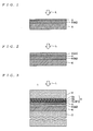
- FIG. 1 is a cross-sectional view schematically showing the multilayer structure of an optical recording medium according to a first aspect of the present invention.
- FIG. 2 is a cross-sectional view schematically showing the multilayer structure of an optical recording medium according to a second aspect of the present invention.
- FIG. 3 is a cross-sectional view of an optical recording medium 1 fabricated using the multilayerstructure according to the second aspect of the present invention.
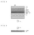
- FIG. 4 is a cross-sectional view of an optical recording medium 1A fabricated using the multilayer structure according to the second aspect of the present invention.
- FIG. 5 is a cross-sectional view of a state where a first dielectric layer 3 (a first absorbing layer A1) is formed on the recording layer 4.
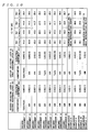
- FIG. 6 is a table showing the construction of respective optical recording media fabricated as the first embodiment and evaluation results for cross-erasing and reproduction durability.
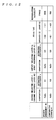
- FIG. 7 is a table showing the construction of respective optical recording media fabricated as the second embodiment and evaluation results for cross-erasing and reproduction durability.
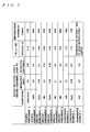
- FIG. 8 is a table showing the construction of respective optical recording media fabricated as the third embodiment and evaluation results for jitter.
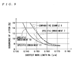
- FIG. 9 is a graph showing the relationship between the shortest mark lengths Ms and the occurrence of jitter for specific embodiments 10 and 11 and comparative examples 6 and 7 for the third embodiment.
- FIG. 10 is a table showing the construction of respective optical recording media fabricated as the fourth embodiment and evaluation results for C/N ratios of the reproduction signals.
- FIG. 11 is a table showing the construction of respective optical recording media fabricated as the fifth embodiment and evaluation results for C/N ratios of the reproduction signals.
- FIG. 12 is a table showing the construction of respective optical recording media fabricated as the sixth embodiment and evaluation results for cross-erasing and reproduction durability.
- a recording layer 4 when looking from an incident side for laser light L (referred to as "recording light or reproduction light” for the present invention), a recording layer 4, a second dielectric layer 5, and a heat sink layer 6 are formed in that order.
- a first dielectric layer 3 when looking from an incident side for laser light L, a first dielectric layer 3, a recording layer 4, a second dielectric layer 5, and a heat sink layer 6 are formed in that order.
- the second dielectric layer 5 corresponds to a "first absorbing layer” for the present invention and the first dielectric layer 3 corresponds to a "second absorbing layer” for the present invention.
- the first dielectric layer 3 is referred to as the first absorbing layer A1 and the second dielectric layer 5 as the second absorbing layer A2.
- the first absorbing layer A1 and the second absorbing layer A2 (hereinafter referred to as the "absorbing layers A" when no distinction is required) are formed so that when the complex refractive index is expressed as (n+ik (where n is a refractive index)), an extinction coefficient k for the wavelength of the laser light L is in a range of 0.06 to 1.0, inclusive.
- the absorbing layers A are formed so that the extinction coefficient k is zero, the effect of the present invention is not realized, while when the absorbing layers A are formed so that the extinction coefficient k is a large value that exceeds 1.0, the absorptance for the laser light L in the absorbing layers A is too high, which obstructs the recording and reproduction of recording information.
- the extinction coefficient k of the absorbing layers A can be calculated based on the reflectivity and transmissivity for the absorbing layers A. More specifically, as one example, the extinction coefficient k can be calculated according to the procedure shown below.
- the measurement sample A-1 is fabricated by forming an absorbing layer A with a thickness of 20nm on a glass slide.
- a measurement sample A-2 is fabricated by forming an absorbing layer A with a thickness of 20nm and a reflective layer with a thickness of 100nm in that order on a glass slide. It should be noted that an optical material whose complex refractive index (n+ik) is known is used as the reflective layer of the measurement sample A-2.
- the reflectivity and transmissivity for the wavelength of the laser light L are measured for the measurement samples A-1 and A-2, respectively.
- the measurement of the reflectivity and transmissivity is carried out using a 45° absolute reflectivity measurement accessory (RTA-2000 type) for a spectrophotometer (MPS-2000) made by Shimadzu Corporation, for example.
- RTA-2000 type 45° absolute reflectivity measurement accessory
- MPS-2000 spectrophotometer
- the complex refractive index is found by the matrix method.
- the extinction coefficient k is specified using this complex refractive index. It should be noted that the complex refractive index is not limited to being calculated by the method described above, and can be found using an ellipsometer or the like.
- the laser light L passes through the recording layer 4 and the second dielectric layer 5 (the second absorbing layer A2) and is reflected by the heat sink layer 6, before passing back through the second dielectric layer 5 and reaching the recording layer 4.
- the second dielectric layer 5 absorbs part of the laser light L and generates heat, so that compared to a conventional optical recording medium that does not have a second dielectric layer 5, the generation of heat by the recording layer 4 is suppressed.
- the second dielectric layer 5 is present between the heat sink layer 6, which favorably dissipates heat, and the recording layer 4, so that the heat generated in the second dielectric layer 5 is conducted to the heat sink layer 6 and is quickly dissipated.
- the effect described above can be sufficiently obtained when the relationship between the wavelength ⁇ of the laser light L (recording/reproduction light) and the numerical aperture NA of the irradiation optical system of the laser light L is ⁇ /NA ⁇ 680nm and preferably ⁇ /NA ⁇ 630nm.
- ⁇ /NA correlates to the beam spot diameter of the laser light L so that the beam spot diameter becomes smaller as ⁇ /NA falls, so that as a result, the energy density inside the beam spot rises. Also, as described above, normally if the energy density inside the beam spot rises, the reproduction durability falls and cross-erasing becomes likely.
- ⁇ /NA is a relatively small value as described above, it is possible to improve the reproduction durability and to also reduce cross-erasing.
- there are limits on the laser wavelength and the numerical aperture that can be used with it being difficult to set an extremely low wavelength and an extremely high numerical aperture. For this reason 250nm ⁇ /NA, and preferably 350nm ⁇ /NA is set.
- the multilayer structure of the optical recording medium according to the present invention is effective when ⁇ /NA is in the above range and the recording track pitch Pt is such that Pt ⁇ 0.35 ⁇ m, and in particular Pt ⁇ 0.33 ⁇ m.
- the recording track pitch Pt is such that Pt ⁇ 0.35 ⁇ m, and in particular Pt ⁇ 0.33 ⁇ m.
- the lower limit of the recording track pitch Pt since there are limits on the laser wavelength and the numerical aperture that can be used, it is difficult in reality to make the beam spot diameter that correlates to ⁇ /NA extremely small. Accordingly, although 0.14 ⁇ m ⁇ Pt is normally set, it is preferable to set 0.15 ⁇ m ⁇ Pt.
- the first dielectric layer 3 (the first absorbing layer A1) is formed on a nearside surface of the recording layer 4 when looking from the incident side for the laser light L, so that while the reproduction durability is improved with the second dielectric layer 5, a further reduction in jitter is achieved by the first dielectric layer 3.
- the optical recording medium according to the second aspect when the shortest mark length Ms for recording marks is set at Ms ⁇ 0.17 ⁇ m, a sufficient reduction in jitter can be achieved compared to other optical recording media.
- the optical recording medium according to the second aspect is especially effective as an optical recording medium for high-density recording. It should be noted that there is no clear reason why jitter is reduced when the shortest mark length Ms is the value given above.
- the absorbing layers A should preferably be formed by sputtering. It should be noted that the absorbing layers A may be composed of a plurality of layers of different compositions.
- the thickness of the absorbing layers A can be decided as appropriate to facilitate optical design and thermal design for the entire optical recording medium in a range within which the reproduction durability can be improved and the jitter can be reduced. As one example, the thickness of the absorbing layers A may be set at 5nm to 50nm, inclusive, or more preferably at 5nm to 40nm, inclusive.
- the absorbing layers A are too thin, it is difficult to improve the reproduction durability and to reduce jitter.
- the absorbing layers A are too thick, there is a fall in the amount of light reflected from the optical recording medium during irradiation with the laser light L, so that it is difficult to obtain a sufficient reproduction output, which makes the reproduction of recorded information problematic.
- the optical material used in the absorbing layers A can be decided as appropriate to facilitate optical design and thermal design for the entire optical recording medium.
- the extinction coefficient k is controlled via the target composition, the flow of the reactive gas during reactive sputtering, and the like.
- the absorbing layers A so as to tightly adhere to the recording layer 4.
- the thickness of such layers is set at 30nm or below, and preferably at 20nm or below.
- the present invention is especially effective for phase-change optical recordingmedia, the invention can also be applied to optical recording media (such as magneto-optical recording media) that use heat mode recording. With such magneto-optical recording media, normally when ⁇ /NA is small, magnetic inversion due to repeated reproduction can easily occur, as can cross-erasing.
- such problems can be effectively avoided.
- Japanese Laid-Open Patent Publication No. S63-217542 discloses an optical information recording member where transparent heat-resistant protective layers are formed so as to sandwich the recording layer and second heat-resistant protective layers that exhibit absorption at the wavelength of the laser light L used for recording and erasing are also formed between the recording layer and the heat-resistant protective layers.
- the second heat-resistant protective layers disclosed in this publication are similar to the absorbing layers A for the present invention in exhibiting absorption at the wavelength of the laser light L.
- the present invention is very different to the invention of this publication.
- the thickness of the light absorbing layers (the recording layer and the protective layers) is larger than in conventional media, resulting in an increase in heat capacity, so that it is possible to make a temperature distribution in the track width direction within the recording track grooves uniform. That is, in the invention disclosed by the publication, as shown by the curve 10 in FIG. 2 of the publication, the region in which the temperature rises due to irradiation with the recording light extends in the width direction for recording tracks and the peak temperature in the center of the recording tracks falls.
- the invention disclosed by the publication differs from the first aspect of the present invention in that no heat sink layer that favorably dissipates heat is provided. Accordingly, in the invention of the publication, since no heat sink layer is provided, the generated heat will accumulate in the protective layers that absorb light, so that as a result, it is thought that the region of the recording layer with raised temperature will extend in the width direction of the recording track to cause cross-erasing.
- recording is carried out using laser light with a wavelength of 830nm and compared to the first aspect of the present invention, the beam spot diameter is large, so that the energy density inside the beam spot is comparatively low.
- an optical recording medium 1 has the heat sink layer 6 that is made of a metal or a metalloid, the second dielectric layer 5 (the second absorbing layer A2), the recording layer 4 that is a phase change layer, the first dielectric layer 3, and the translucent substrate 2 formed in that order in layers on a support substrate 7.
- the laser light L (recording/reproduction light) is incident from the surface on which the translucent substrate 2 is formed.
- an intermediate layer composed of a dielectric material may be provided between the support substrate 7 and the heat sink layer 6, an intermediate layer composed of a dielectric material may be provided.
- the support substrate 7 keeps the optical recording medium 1 rigid, and has grooves and lands (not shown) formed in a surface thereof.
- the thickness of the support substrate 7 is normally 0.2 to 1.2mm and preferably 0.4 to 1.2mm, and the support substrate 7 may be transparent or opaque.
- the support substrate 7 may be formed using a resin such as polycarbonate in the same way as a normal optical recording medium, or may be formed of glass.
- the heat sink layer 6 is a layer for taking the heat generated by the second dielectric layer 5 and quickly conducting the heat to the support substrate 7, and is formed on the surface of the support substrate 7 by sputtering or a vapor phase epitaxymethod such as vapor deposition.
- a metal or metalloid such as Al, Au, Ag, Pt, Cu, Ni, Cr, Ti, and Si, or an alloy including one or more of such elements may be used.
- Ag or Al alone sufficient corrosion resistance is not achieved, so that an element that improves the corrosion resistance should preferably be added.
- the surface roughness on the incident-side for the laser light L is likely to increase, which can cause increases in reproduction noise. Accordingly, when the heat sink layer 6 is formed, it is preferable to make the crystal grain diameter small, so that instead of using Ag or Al alone, an element for reducing the crystal grain diameter of the heat sink layer 6 or for making the heat sink layer 6 an amorphous layer should preferably be added.
- the heat sink layer 6 With Ag, which has high heat conductivity, as a main constituent so that the recording layer 4 and the second dielectric layer 5 can be quickly cooled during irradiation with the laser light L.
- Ag which has high heat conductivity
- Mg, Pd, Ce, Cu, Ge, La, S, Sb, Si, Te, and Zr can be given as examples of additional component elements added to the Ag. It is preferable for at least one and more preferably two or more of such additional component elements to be used.
- the included amounts of the additional component elements in the heat sink layer 6 are set so that the added amount of any single element is 0.05 to 2.0% by atoms and preferably 0.2 to 1. 0% by atoms and the total additional component amount is 0.2 to 5.0% by atoms and preferably 0.5 to 3.0% by atoms. In this case, if the included amount of the additional component elements is too small, the effect (such as a reduction in surface roughness) of the inclusion of such additional component elements is insufficient. On the other hand, if the amount of the included additional component elements is too large, the heat conductivity falls.
- the heat conductivity of the heat sink layer 6 composed of a metal or metalloid tends to decrease as the crystal grain diameter falls. For this reason, if the heat sink layer 6 is amorphous, it is difficult to obtain a sufficient cooling speed during recording, so that it is preferable to initially form the heat sink layer 6 as an amorphous layer and to then crystallize the heat sink layer 6 by performing a heat treatment. In this case, by crystallizing the heat sink layer 6 by performing a heat treatment after initially forming an amorphous layer, the surface roughness (smoothness) of the amorphous state can be maintained, and the heat conductivity can also be improved by the crystallization.
- the thickness should preferably be set at 10nm to 300nm, inclusive.
- the heat sink layer 6 may be formed of other materials.
- the heat sink layer 6 may be formed of other materials.
- the laser light L is incident via the recording layer 4 on the surface side, and when a heat sink layer 6 made of metal is provided on this surface-side recording layer 4, the present of the heat sink layer 6 causes a remarkable fall in the transmissivity for the laser light L.
- a relatively thick resin layer is often provided between the recording layers 4, 4.
- a resin layer with a certain degree of thickness has a relatively high thermal capacity, so that when the present invention is applied to a multilayer optical recording medium, the above resin layer is used as the heat sink layer for the present invention.
- the first dielectric layer 3 and the second dielectric layer 5 are formed by sputtering or the like to sandwich the recording layer 4, so that oxidization and deterioration of the recording layer 4 are prevented and heat conducted from the recording layer 4 during irradiation with the laser light L is cut off and conducted away in the planar direction, thereby protecting the support substrate 7 and the translucent substrate 2. Also, by providing the first dielectric layer 3 and the second dielectric layer 5, it is possible to improve the modulation degree of the laser light L.
- the second dielectric layer 5 corresponds to the first absorbing layer for the present invention, and as described later is formed as a thin film of an optical material.
- the second dielectric layer 5 is formed so that the entire layer in the thickness direction functions as the second absorbing layer A2, but this is not a limitation for the present invention and, like the first dielectric layer 3, the second dielectric layer 5 may have a multilayer structure of a plurality of unitary dielectric layers, with at least one layer out of the unitary dielectric layers being set as the second absorbing layer A2. In this case, it is preferable for the unitarydielectric layers aside from the second absorbing layer A2 to have a heat conductivity that is equal to or higher than the heat conductivity of the second absorbing layer A2.
- the first dielectric layer 3 is composed of a plurality of unitary dielectric layers 3a to 3c with different compositions that are formed on top of one another.
- the unitary dielectric layer 3c (the first absorbing layer A1) formed on the recording layer 4 functions as the second absorbing layer for the present invention.
- the first dielectric layer 3 can also be formed of a single film whose entire thickness can be used as the first absorbing layer A1.
- the first dielectric layer 3 used as the first absorbing layer A1 is too thick, the amount of reflected light for the laser light L is reduced and it becomes difficult to obtain a sufficient reproduction output, so that the first dielectric layer 3 shouldpreferablybe formed with an overall thickness of 50nm or below. Accordingly, as shown in FIG. 3, it is normally preferable for the first dielectric layer 3 to be formed of a multilayer structure such as the plurality of unitary dielectric layers 3a to 3c, with one unitary dielectric layer out of the layers 3a to 3c being set as the first absorbing layer A1.
- the dielectrics (optical materials) used as the second dielectric layer 5 and the unitary dielectric layers 3a to 3c (the first dielectric layer 3) are preferably compounds including at least one kind of metal component selected from Si, Ge, Zn, Al, and rare earth elements, for example. Such compounds should preferably be oxides, nitrides, or sulfides, and it is alsopossible to use amixture including two or more of such compounds.
- the respective thicknesses of the first dielectric layer 3 and the second dielectric layer 5 may be determined as appropriate so that the protective effect and modulation degree improving effect are sufficiently obtained, with the thickness of the first dielectric layer 3 normally being set in a range of 30nm to 300nm, inclusive, and preferably 50nm to 250nm, inclusive, and the thickness of the second dielectric layer 5 being set in a range of 5nm to 50nm, inclusive.
- the thickness of the second dielectric layer 5 is set at 30nm or below, and preferably at 25nm or below.
- the recording layer 4 is formed by sputtering a phase change material and various recording information is recorded by forming recording marks by irradiation with laser light L of the recording power.
- various recording information is recorded by forming recording marks by irradiation with laser light L of the recording power.
- the composition of the recording layer 4 there are no particular limitations on the composition of the recording layer 4, but it is preferable for at least Sb and Te to be included.
- the recording layer 4 composed of only Sb and Te has an extremely low crystallization temperature of around 130°C and the storage reliability of the recorded information is insufficient, so that other elements should preferably be added to improve the crystallization temperature.
- Mn, In, Ag, Au, Bi, Se, Al, P, Ge, H, Si, C, V, W, Ta, Zn, Ti, Sn, Pb, Pd, and rare earth elements (Sc, Y and lanthanides) can be given as examples of such added elements.
- the elements aside from Sb and Te are expressed as "M", and it is preferable for the conditions given below to be satisfied when the atomic ratio of the elements composing the recording layer is expressed as Equation (1) below.
- (Sb x Te 1-x ) 1-y M y where preferably 0.2 ⁇ x ⁇ 0.9 and 0 ⁇ y ⁇ 0.4. More preferably, x and y should be set so that 0.5 ⁇ x ⁇ 0.85 and 0.01 ⁇ y ⁇ 0.2.
- Equation (1) above when the value x that represents the included amount of Sb is too small, the crystallization speed is reduced, so that it is difficult to erase recordingmarks at relatively high linear velocities and the reflectivity of crystallized regions of the recording layer 4 also falls, thereby reducing the reproduction signal output. Also, when x is too small, the recording of information (i.e., the formation of recording marks) becomes difficult, while when x is too large, the difference in reflectivity between the crystallized state and the amorphous state is reduced, which reduces the reproduction signal output. On the other hand, although there are no limitations for the element M, at least one of the above elements that exhibit the storage reliability improving effect should preferably be selected.
- the thickness of the recording layer 4 should preferably be set in a range of 4nm to 50nm, inclusive, with a range of 5nm to 30nm, inclusive being even more preferable. In this case, when the recording layer 4 is too thin, it becomes difficult for the crystal phase to grow, so that crystallization becomes difficult. On the other hand, if the recording layer 4 is too thick, the heat capacity of the recording layer becomes large, so that the recording of information becomes difficult and the reproduction signal output also falls.
- the translucent substrate 2 is formed of a resin plate or a glass plate of around the same thickness as the support substrate 7 and can transmit the laser light L. It should be noted that to achieve a high recording density by raising the numerical aperture NA, the translucent substrate 2 should preferably be made thin. The thickness of the translucent substrate 2 should also preferably be set in a range of 30 ⁇ m to 300 ⁇ m, inclusive. In this case, when the translucent substrate 2 is too thin, dust and the like adhering to the surface of the translucent substrate 2 has a larger effect. Conversely, when the translucent substrate 2 is too thick, it becomes difficult to achieve a high recording density by increasing the numerical aperture NA.
- the translucent substrate 2 it is possible to form the translucent substrate 2 by sticking a light transmitting resin sheet composed of a translucent resin onto the first dielectric layer 3 using various kinds of adhesive or glue, or by applying a resin in a thin film to form a translucent resin layer (the translucent substrate 2) directly on the first dielectric layer 3.
- the laser light L used to irradiate the medium 1 when recording information passes through the translucent substrate 2, the first dielectric layer 3, the recording layer 4, and the second dielectric layer 5, is reflected by the heat sink layer 6, and then passes back through the second dielectric layer 5 to reach the recording layer 4.
- the unitary dielectric layer 3c and the second dielectric layer 5 respectively absorb part of the laser light L and generate heat, so that compared to the case where the unitary dielectric layer 3c and the second dielectric layer 5 are not provided, the generation of heat by the recording layer 4 can be suppressed.
- the unitary dielectric layer 3c (the first dielectric layer 3) is present between the translucent substrate 2 and the recording layer 4, and the second dielectric layer 5 is present between the heat sink layer 6, which favorably dissipates heat, and the recording layer 4 so that the heat generated in the unitary dielectric layer 3c is conducted to the translucent substrate 2 and quickly dissipated and the heat generated in the second dielectric layer 5 is conducted to the heat sink layer 6 and quickly dissipated.
- the generation of heat by the unitary dielectric layer 3c and the second dielectric layer 5 hardly affects the recording layer 4. Accordingly, with the optical recording medium 1, it is possible to reduce jitter and to also increase the reproduction durability.
- the heat generated by the second dielectric layer 5 is conducted to the heat sink layer 6 and quickly dissipated, so that when the recording layer 4 is irradiated with the laser light L, the region that is heated to a relatively high temperature is limited to the beam spot and only the narrow immediate periphery of the beam spot. Accordingly, the occurrence of cross-erasing can be avoided with the optical recording medium 1.
- This optical recording medium 1A includes a first dielectric layer 3, a recording layer 4, a second dielectric layer 5, a heat sink layer 6, and a protective layer 2A formed in that order on a support substrate 7, with the recording and reproduction of information being carried out by irradiation with laser light L from the support substrate 7 side.
- the support substrate 7 may be formed in the same way as the optical recording medium 1 described above, though the support substrate 7 needs to be formed of a translucent material that can transmit the laser light L.
- the protective layer 2A is provided to improve the scratch resistance and corrosion resistance.
- the protective layer should preferably be formed from a variety of organic substances, and in particular it is preferable to use a substance produced by curing a radiation curing compound or a composite of the same using radiation such as microwaves or UV rays.
- the protective layer 2A normally has a thickness in a range of 0.1 ⁇ m to 100 ⁇ m, inclusive, and is formed by a conventional method such as spin coating, gravure coating, spray coating, and dipping. It should be noted that the other layers that are the same as the corresponding component parts of the optical recording medium 1 have been given the same reference numerals and duplicated description thereof has been omitted.
- the laser light L used to irradiate the optical recording medium 1A during the recording of information passes through the support substrate 7, the first dielectric layer 3, the recording layer 4, and the second dielectric layer 5, is reflected by the heat sink layer 6, and then passes back through the second dielectric layer 5 to reach the recording layer 4.
- the unitary dielectric layer 3c and the second dielectric layer 5 respectively absorb part of the laser light L and generate heat, so that in the same way as the optical recording medium 1 described above, compared to the case where the unitary dielectric layer 3c (the first dielectric layer 3) and the second dielectric layer 5 are not provided, the amount of heat generated by the recording layer 4 can be suppressed.
- the first dielectric layer 3 is present between the support substrate 7 and the recording layer 4 and the second dielectric layer 5 is present between the heat sink layer 6, which favorably dissipates heat, and the recording layer 4, so that the heat generated in the unitary dielectric layer 3c is conducted to the support substrate 7 and quickly dissipated and the heat generated in the second dielectric layer 5 is conducted to the heat sink layer 6 and quickly dissipated to the protective layer 2A.
- the heat generated by the unitary dielectric layer 3c and the second dielectric layer 5 hardly affects the recording layer 4. Accordingly, with the optical recording medium 1A, it is possible to reduce jitter and to also increase the reproduction durability.
- the heat generated by the second dielectric layer 5 is conducted to the heat sink layer 6 and quickly dissipated, so that when the recording layer 4 is irradiated with the laser light L, the region that is heated to a relatively high temperature is limited to the beam spot and only the narrow immediate periphery of the beam spot. Accordingly, the occurrence of cross-erasing can also be avoided with the optical recording medium 1A.
- the second dielectric layer 5 (the second absorbing layer A2) is formed on one surface of the recording layer 4 and the unitary dielectric layer 3c (the first absorbing layer A1) is formed on the other surface
- the first dielectric layer 3 (the first absorbing layer A1) as the second absorbing layer for the present invention on only one surface of the recording layer 4.
- the present inventors have also confirmed that with the stated multilayer structure (a structure with no second dielectric layer 5), reproduction durability can be improved and the occurrence of cross-erasing can be reduced.
- the first dielectric layer 3 is provided on the nearside of the recording layer 4 in the incident direction
- the second dielectric layer 5, and the heat sink layer 6 are formed in that order from the incident direction of the laser light L as in the optical recording medium according to the present invention
- the first absorbing layer for the present invention is formed on the deeper side of the recording layer 4 with respect to the incident direction.
- Optical recording media according to specific embodiments 1 and 2 and a comparative example 1 shown in FIG. 6 were fabricated as described below and the occurrence of cross-erasing and reproduction durability were evaluated for such media. It should be noted that the respective optical recording media have the same construction as the optical recording medium 1 shown in FIG. 3.
- a polycarbonate disc with a diameter of 120mm and a thickness of 1.2mm in which grooves are formed during injection molding is used as the support substrate 7.
- the recording track pitch for a land/groove recording method is set at 0.3 ⁇ m.
- the heat sink layer 6 is formed with a thickness of 100nm by sputtering in an Ar atmosphere.
- the second dielectric layer 5 is formed with a thickness of 12nm by sputtering.
- the composition of the second dielectric layer 5 and the extinction coefficient k are shown in FIG. 6.
- the complex refractive indices of the compositions shown in FIG. 6 are CeO 2 :2.7+0.1i, ZnO:2.3+0.1i, and Al 2 O 3 :1.76+0i.
- the complex refractive indices of the respective absorbing layers were measured using a 45° absolute reflectivity measurement accessory (RTA-2000 type) for a spectrophotometer (MPS-2000) made by Shimadzu Corporation.
- the recording layer 4 is formed with a thickness of 12nm by sputtering with an alloy target in anAr atmosphere.
- the first dielectric layer 3 is formed with a thickness of 50nm by sputtering with a ZnS (80mol%)-SiO 2 (20mol%) target in an Ar atmosphere.
- the translucent substrate 2 is formed by spin coating the surface of the first dielectric layer 3 with a UV curing resin and hardening the resin.
- the optical recording media were placed in an optical recording medium evaluation apparatus and cross-erasing was measured using the procedure described below with the following conditions
- the value ⁇ /NA is set at 476nm.
- the measured track was overwritten ten times with an 8T signal, and the carrier output was set as C1.
- both adjacent tracks for the measured track were overwritten respectively one hundred times with a 7T signal.
- the carrier output for the 8T signal originally recorded on the measured track was measured again and set as C2.
- the value C2 - C1 is the cross-erasing.
- the recording power and erasing power used when overwriting the measured track is an optimal value (a value that minimizes jitter) for the specific embodiments 1 and 2 and the comparative example 1.
- values 30% in excess of the optimal values for the specific embodiments 1 and 2 and the comparative example 1 were used as the recording power and erasing power when overwriting both adjacent tracks for the measured track.
- FIG. 6 shows the cross-erasing when grooves (G) are set as the measured tracks and the cross-erasing when lands (L) are set as the measured tracks.
- the reproduction durability was measured for the specific embodiments 1 and 2 and the comparative example 1.
- a mixed signal was recorded at the optimal recording power on the measured track (grooves) with the same conditions as the measurement of cross-erasing, reproduction was carried out repeatedly with a power of 0.5mW, and the maximum number of reproduction repetitions for which jitter does not worsen was investigated. The results are shown in FIG. 6.
- Optical recording media according to specific embodiments 3 to 9 and comparative examples 2 to 4 shown in FIG. 7 were fabricated in the same way as the first embodiment described above, and the occurrence of cross-erasing and the reproduction durability of these media were evaluated in the same way as the first embodiment.
- a grooved recording substrate (with a track pitch of 0.32 ⁇ m and a groove depth of 22nm) was used as the support substrate 7.
- the AlN of the second dielectric layer 5 in the specific embodiments 8 and 9 and the comparative examples 2 and 4 is formed by reactive sputtering of Ar and N 2 , and by varying the proportions of the Ar and N 2 , optical recording media with different extinction coefficients k were manufactured.
- the recording characteristics of an optical recording medium are normally affected when the cross-erasing exceeds -1.0dB.
- the extinction coefficient k of the second dielectric layer 5 (the second absorbing layer A2) is set in a range of 0.06 to 1.0 inclusive
- the comparative example 2 with an extinction coefficient k of zero and the comparative example 3 with an extinction coefficient k of 0.01 there is much cross-erasing and a large decrease in reproduction durability.
- the comparative example 4 with an extinction coefficient k of 1.2 the reproduction output is small, so that reproduction is problematic and in turn it is difficult to even evaluate the occurrence of cross-erasing and the reproduction durability.
- the extinction coefficient k of the first absorbing layer for the present invention in this case, the second dielectric layer 5 in a range of 0.06 to 1.0, inclusive, it is possible to manufacture an optical recording medium with little jitter and favorable reproduction durability.
- Optical recording media according to specific embodiments 10 and 11 and comparative examples 5 to 7 shown in FIG. 8 were fabricated as described below, and the occurrence of cross-erasing was evaluated for such media. It should be noted that these optical recording media were fabricated with the same construction as the optical recording medium 1 shown in FIG. 3.
- the support substrate 7, the heat sink layer 6, the recording layer 4, and the translucent substrate 2 were formed in the same way as in the first embodiment.
- the second dielectric layer 5 (the second absorbing layerA2) was formed with a thickness of 12nm by sputtering.
- the composition and extinction coefficient k of the second dielectric layer 5 are shown in FIG. 8.
- the second dielectric layer 5 (in the specific embodiments 10 and 11) whose extinction coefficient k is 0.1 functions as the second absorbing layer A2 (the first absorbing layer for the present invention).
- a second dielectric layer 5 made of ZnO is formed by sputtering a ZnO target in an Ar gas atmosphere.
- the second dielectric layer 5 made of ZnO+O (in the comparative example 7) is formed by reactive sputtering of a ZnO target in an Ar gas atmosphere including oxygen gas.
- the complex refractive index of the ZnO+O is set as ZnO+O:2.2 +0i.
- the unitary dielectric layer 3c (the first absorbing layer A1) out of the first dielectric layer 3 was formed with a thickness of 10nm.
- the composition and extinction coefficient k of this unitary dielectric layer 3c are shown in FIG. 8. It should be noted that in the comparative examples 6 and 7, a dielectric layer with an extinction coefficient k of zero was formed in place of the unitary dielectric layer 3c.
- the unitary dielectric layer 3b out of the first dielectric layer 3 has a thickness of 25nm and is composed of ZnS (80mol%)-SiO 2 (20mol%).
- the unitary dielectric layer 3a out of the first dielectric layer 3 has a thickness of 60nm and is composed of Al 2 O 3 .
- the optical recording media were placed in an optical recording medium evaluation apparatus and jitter was measured with the following conditions
- clock jitter The jitter referred to here is so-called "clock jitter”.
- a reproduction signal is measured by a time interval analyzer, the "fluctuation ( ⁇ ) in the signal” is found, and jitter is the value calculated based on ⁇ /Tw(%) using a detection window width Tw.
- the results are shown in FIG. 8.
- the results for some of the samples are also shown in FIG. 9. In this case, when jitter is 12% or below, the errors are within tolerance and the reproduction of recording information is possible. Also, to sufficiently maintain various margins, jitter should preferably be 10% or below.
- the jitter is below 10% for the specific embodiments 10 and 11 and the comparative examples 5 to 7.
- the shortest mark Ms is set at 0.147 ⁇ m
- jitter is favorable at below 12%
- jitter exceeds 13%.
- the extinction coefficient k of the second absorbing layer for the present invention (in this case, the unitary dielectric layer 3c) at 0.06 or above, it is possible to manufacture an optical recording medium with little jitter.
- the extinction coefficient k of the unitary dielectric layer 3c is 0.1
- the extinction coefficient k of the second dielectric layer 5 is set at zero (as in the comparative example 5)
- the jitter is 12.9% when the shortest mark length Ms is 0.147 ⁇ m.
- the respective extinction coefficients k of the first and second absorbing layers for the present invention at 0.06 or above, it is possible to manufacture an optical recording medium with less jitter.
- the effect of the present invention is realized in the specific embodiment 11 provided with absorbing layers made of ZnO, the effect of the invention is not realized with the comparative example 7 where oxygen is excessively added to the ZnO and the extinction coefficient k falls. From this, it is clear that the effect of the present invention does not depend on the composite elements of the absorbing layers and instead depends on the extinction coefficient k.
- Optical recording media according to specific embodiments 12 to 20 and comparative examples 8 to 11 shown in FIG. 10 were fabricated in the same way as the third embodiment described above, and the C/N ratio was measured for these media.
- a grooved recording substrate (withatrackpitch of 0.32 ⁇ m and a groove depth of 22nm) was used as the support substrate 7.
- the thickness of the unitary dielectric layer 3c was set at 30nm. In this case, if the C/N ratio is 35dB or above, it will normally be possible to reproduce the recorded information (i.e., to read the recording marks) with current signal processing technology, which means the media can be used as an actual optical recording media.
- the C/N ratio is a high value of 35dB or above for the respective shortest mark lengths Ms, so that the recorded information can be properly reproduced.
- the comparative examples 8 and 11 where the extinction coefficient k of one of the second dielectric layer 5 and the unitary dielectric layer 3c is 1.2, the reproduction output is low and reproduction is difficult, resulting in difficulty even in measuring the C/N ratio.
- the C/N ratio falls to 30.5dB when the shortest mark length Ms is 0.138 ⁇ m, so that proper reproduction of the recorded information becomes difficult.
- the C/N ratio falls to 30.
- Optical recording media according to a specific embodiment 21 and a comparative example 12 shown in FIG. 11 were fabricated in the same way as the fourth embodiment described above, and the C/N ratio for these media was measured. It should be noted that the AlN of the unitary dielectric layer 3c of this fifth embodiment was formed by reactive sputtering inAr and N 2 , and optical recording media with different extinction coefficients k were fabricated by varying the proportions of Ar and N 2 .
- the C/N ratio for all of the shortest mark lengths Ms is 35db or above, so that the recorded information can be properly reproduced.
- the C/N ratio falls to 31.2dB, so that it is difficult to reproduce the recorded information properly. That is, even when the same material is used, so long as the extinction coefficient k of such material does not satisfy the condition of the present invention, the effect of the present invention cannot be obtained.
- the respective extinction coefficients k of the first and the second absorbing layers for the present invention in a range of 0.06 to 1. 0, inclusive, it is possible to manufacture an optical recording medium (that can be properly reproduced) with a high C/N ratio.
- this optical recording medium by constructing the first absorbing layer so that the extinction coefficient k is in a range of 0.06 to 1.0, inclusive, for the wavelength of the light used for recording and reproduction, it is possible to sufficiently improve the reproduction durability and to sufficiently reduce cross-erasing, even when recording at high density. By doing so, it is possible to realize an optical recording medium that can be recorded at high density, has high reproduction durability, and is not susceptible to cross-erasing.
Abstract
The optical recording medium according to the present
invention includes a recording layer (4), a second absorbing
layer (A2) and a heat sink layer (6) formed in order from
an incident side for laser light (L), the second absorbing
layer (A2) having an attenuation coefficient k for a
wavelength of the laser light (L) that satisfies 0.06≦k
≦1.0. In this case, a first absorbing layer (A1) is
preferably formed on an incident side-surface of the
recording layer (4) for the laser light (L), the first
absorbing layer (A1) having an attenuation coefficient k
for the wavelength of the laser light (L) that satisfies
0.06≦k≦1.0. By doing so, even when recording at high
density, it is possible to sufficiently improve the
reproduction durability and to sufficiently reduce the
cross-erasing.
Description
The present invention relates to an optical
recording medium constructed so that the recording or
reproduction of information can be carried out by irradiation
with recording light or reproduction light.
Optical recording media that are capable of
high-density recording and on which recorded information
can be deleted and overwritten (hereinafter referred to as
"rewritable optical recording media") have been subject to
much attention in recent years. Information is recorded
on phase-change optical recording media, which are one
example of such rewritable optical recording media, by
changing the crystal state of a recording layer through
irradiation with laser light. Recorded information is
reproduced by detecting changes in the reflectivity of the
recording layer due to such changes in the crystal state.
Phase-change optical recording media have been subject to
particular attention since it is possible to record and
reproduce information using an optical system with a simpler
construction than an optical system used with
magneto-optical recording media. In this case, in a
phase-change optical recording medium, chalcogenide
compounds, such as Ge-Sb-Te materials, are normally used
as the optical material of the recording layer for reasons
such as the large difference in the reflectivity between
the crystal state and the amorphous state and also the
relatively high stability of suchmaterials in the amorphous
state.
When information is recorded on a phase-change
optical recording medium, the recording layer is irradiated
by laser light (a recording laser beam) set at a high power
(the "recording power") capable of raising the temperature
of the recording layer to the melting point or above. By
doing so, amorphous recording marks are formed at the
positions that were irradiated by the laser light of the
recording power through rapid cooling after the recording
layer has melted. Also, when erasing recording marks, the
marks are irradiated by laser light of relatively low power
(the "erasing power") that is capable of raising the
temperature of the recording layer to the crystallization
temperature or above but below the melting point. In this
case, the parts that were irradiated by the laser light of
the erasing power are slowly cooled after the recording layer
has been heated to the crystallization temperature or above,
so that the recording marks (amorphous parts) are restored
to the crystal state (i.e., the recording marks are erased) .
In this way, by varying the power (irradiating power) of
a single laser beam, it is possible to overwrite the recording
data on a rewritable phase-change optical recording medium.
On the other hand, to realize a high recording
density, there is a tendency in recent years for optical
recording media to have a reduced track pitch. Also, with
regard to the laser light used to irradiate optical recording
media during recording and reproduction, progress has been
made in reducing the wavelength of the light and increasing
the numerical aperture of an objective lens of a
recording/reproduction optical system that emits the laser
light to make it possible to record and reproduce smaller
recording marks. Accordingly, it has become possible to
increase the amount of information that can be recorded on
a single optical recording medium (i.e., high density
recording has been realized). In this case, the spot
diameter of the recording laser beam emitted onto the surface
of the recording layer is expressed as λ/NA where λ is the
wavelength of the laser light and NA is the numerical aperture
of the objective lens, and as this value λ/NA becomes smaller,
it becomes possible to record and reproduce smaller recording
marks and also possible to carry out recording and
reproduction of an optical recording medium with a narrower
track pitch.
By investigating the conventional optical recording
media described above, the present inventors discovered the
following problems. That is, with a conventional optical
recording medium, to make the overwriting of recorded data
possible, the recording layer is constructed so that
amorphous parts (recording marks) can be restored to the
crystalline state (i.e., the recording marks can be erased)
by irradiation with laser light of the erasing power. For
this reason, to prevent recording marks from being erased
by a reproduction laser beam emitted during the reproduction
of recorded information on this kind of optical recording
medium, a low power laser light that does not affect the
crystalline state of the recording marks is normally used.
However, even if low power laser light, for example, is used
as the reproduction light (the reproduction laser beam),
when the reproduction of the recorded information has been
carried out several times, for some reason recrystallization
(returning to the crystalline state) occurs at parts where
the recording marks are formed. Due to such
recrystallization, there is the problem of an increase in
jitter, that is, there is a large decrease in reproduction
durability. Here, regarding the causes of such
recrystallization, the inventors found that when an optical
recording medium is irradiated with short wavelength laser
light using an optical system with an objective lens with
a large numerical aperture, that is, when the (λ/NA) value
described above is small, recrystallization occurs due to
the energy density increasing inside the laser beam spot.
Accordingly, although it may be thought that jitter can be
reduced using laser light with a large (λ/NA) value, in such
case there is the problem of it being difficult to raise
the recording density.
Also with a conventional optical recording medium,
recrystallization or so-called "cross-erasing" occurs for
recording marks (amorphous parts) formed in tracks that are
adjacent to the trackbeing recorded (hereinafter such tracks
are referred to as "adjacent tracks"), and there is the
problem of the C/N ratio falling due to the occurrence of
such cross-erasing. More specifically, during the
recording of information, when an optical recording medium
is irradiated with laser light of the recording power, the
temperature will rise in the adjacent tracks as well as the
track being recorded through the irradiation of the laser
light. At this time, recording marks formed in the adjacent
tracks are recrystallized. Here, it is known that
cross-erasing becomes more likely when the track pitch of
the tracks being recorded is narrow relative to the spot
diameter of the laser beam. Accordingly, although it is
thought that the occurrence of cross-erasing can be avoided
by reducing the spot diameter of the laser beam, the inventors
found that even if the relationship between the track pitch
of the tracks being recorded and the beam spot diameter is
the same, the higher the energy density inside the beam spot,
for example, the shorter the wavelength of the laser beam
emitted by the recording/reproduction optical system, the
more likely cross-erasing is to occur. For this reason,
it is thought that it will normally be difficult to avoid
the occurrence of cross-erasing by changing the spot diameter
of the laser beam.
The present invention was conceived in order to solve
the problems described above, and it is a principal object
of the present invention to provide an optical recording
medium that can be recorded at high density and can also
improve the reproduction durability and reduce
cross-erasing.
An optical recording medium according to the present
invention includes a recording layer, a first absorbing layer
and a heat sink layer formed in order from an incident side
for light used for recording or light used for reproduction,
the first absorbing layer having an extinction coefficient
k for a wavelength of the light used for recording or the
light used for reproduction that satisfies 0.06≦k≦1.0.
With this optical recording medium, by constructing
the first absorbing layer so that the extinction coefficient
k for the wavelength of the light used for recording or for
reproduction satisfies 0.06≦k≦1.0, it is possible to
sufficiently improve the reproduction durability and to
sufficiently reduce cross-erasing, even when recording at
high density.
Here, the optical recording medium should
preferably include a second absorbing layer formed on an
incident side-surface of the recording layer for the light,
the second absorbing layer having an extinction coefficient
k for the wavelength of the light used for recording or for
reproduction that satisfies 0.06≦k≦1.0. With this
construction, it is possible to further improve the
reproduction durability and to also considerably reduce the
cross-erasing. In this case, jitter can be reduced by an
increasing amount as the shortest mark length used when
recording (i.e., when recording information at high density)
decreases.
It is also preferable for the optical recording
medium to be constructed so as to be capable of being recorded
or reproduced when a relationship between the wavelength
λ of the light used for recording or for reproduction and
a numerical aperture NA of an irradiation optical system
for the light used for recording or for reproduction
satisfies a condition λ/NA≦680nm. With this construction,
information can be recorded with a sufficiently high density
compared to an optical recording medium constructed so as
to be capable of being recorded or reproduced at conditions
that satisfy λ/NA>680nm.
Also, a recording track pitch should preferably be
formed at 0.35µm or below. With this construction,
information can be recorded with a considerably higher
density.
In addition, the optical recording medium should
preferablybe constructed so that information canbe recorded
with a shortest mark length set at 0.17µm or below. With
this construction, information can be recorded at even higher
density.
It should be noted that the disclosure of the present
invention relates to a content of Japanese PatentApplication
2002-117508 that was filed on 19 April 2002 and the entire
content of which is herein incorporated by reference.
FIG. 1 is a cross-sectional view schematically
showing the multilayer structure of an optical recording
medium according to a first aspect of the present invention.
FIG. 2 is a cross-sectional view schematically
showing the multilayer structure of an optical recording
medium according to a second aspect of the present invention.
FIG. 3 is a cross-sectional view of an optical
recording medium 1 fabricated using the multilayerstructure
according to the second aspect of the present invention.
FIG. 4 is a cross-sectional view of an optical
recording medium 1A fabricated using the multilayer
structure according to the second aspect of the present
invention.
FIG. 5 is a cross-sectional view of a state where
a first dielectric layer 3 (a first absorbing layer A1) is
formed on the recording layer 4.
FIG. 6 is a table showing the construction of
respective optical recording media fabricated as the first
embodiment and evaluation results for cross-erasing and
reproduction durability.
FIG. 7 is a table showing the construction of
respective optical recording media fabricated as the second
embodiment and evaluation results for cross-erasing and
reproduction durability.
FIG. 8 is a table showing the construction of
respective optical recording media fabricated as the third
embodiment and evaluation results for jitter.
FIG. 9 is a graph showing the relationship between
the shortest mark lengths Ms and the occurrence of jitter
for specific embodiments 10 and 11 and comparative examples
6 and 7 for the third embodiment.
FIG. 10 is a table showing the construction of
respective optical recording media fabricated as the fourth
embodiment and evaluation results for C/N ratios of the
reproduction signals.
FIG. 11 is a table showing the construction of
respective optical recording media fabricated as the fifth
embodiment and evaluation results for C/N ratios of the
reproduction signals.
FIG. 12 is a table showing the construction of
respective optical recording media fabricated as the sixth
embodiment and evaluation results for cross-erasing and
reproduction durability.
Preferred embodiments of an optical recording
medium according to the present invention will now be
described with reference to the attached drawings.
First, characteristic parts of the present
invention will be described with reference to the drawings.
In a first aspect of the optical recording medium
according to the present invention, as shown in FIG. 1, when
looking from an incident side for laser light L (referred
to as "recording light or reproduction light" for the present
invention), a recording layer 4, a second dielectric layer
5, and a heat sink layer 6 are formed in that order. Also,
in a second aspect of the optical recording medium according
to the present invention, as shown in FIG. 2, when looking
from an incident side for laser light L, a first dielectric
layer 3, a recording layer 4, a second dielectric layer 5,
and a heat sink layer 6 are formed in that order. In this
case, the second dielectric layer 5 corresponds to a "first
absorbing layer" for the present invention and the first
dielectric layer 3 corresponds to a "second absorbing layer"
for the present invention. Here, to make the order in which
the layers are formed more understandable, the first
dielectric layer 3 is referred to as the first absorbing
layer A1 and the second dielectric layer 5 as the second
absorbing layer A2. The first absorbing layer A1 and the
second absorbing layer A2 (hereinafter referred to as the
"absorbing layers A" when no distinction is required) are
formed so that when the complex refractive index is expressed
as (n+ik (where n is a refractive index)), an extinction
coefficient k for the wavelength of the laser light L is
in a range of 0.06 to 1.0, inclusive. As described later,
when the absorbing layers A are formed so that the extinction
coefficient k is zero, the effect of the present invention
is not realized, while when the absorbing layers A are formed
so that the extinction coefficient k is a large value that
exceeds 1.0, the absorptance for the laser light L in the
absorbing layers A is too high, which obstructs the recording
and reproduction of recording information.
In this case, the extinction coefficient k of the
absorbing layers A can be calculated based on the
reflectivity and transmissivity for the absorbing layers
A. More specifically, as one example, the extinction
coefficient k can be calculated according to the procedure
shown below. First, the measurement sample A-1 is
fabricated by forming an absorbing layer A with a thickness
of 20nm on a glass slide. Next, a measurement sample A-2
is fabricated by forming an absorbing layer A with a thickness
of 20nm and a reflective layer with a thickness of 100nm
in that order on a glass slide. It should be noted that
an optical material whose complex refractive index (n+ik)
is known is used as the reflective layer of the measurement
sample A-2. Next, the reflectivity and transmissivity for
the wavelength of the laser light L are measured for the
measurement samples A-1 and A-2, respectively. The
measurement of the reflectivity and transmissivity is
carried out using a 45° absolute reflectivity measurement
accessory (RTA-2000 type) for a spectrophotometer
(MPS-2000) made by Shimadzu Corporation, for example.
Next, based on the reflectivity and transmissivity measured
using the measurement samples A-1 and A-2, the complex
refractive index is found by the matrix method. The
extinction coefficient k is specified using this complex
refractive index. It should be noted that the complex
refractive index is not limited to being calculated by the
method described above, and can be found using an
ellipsometer or the like.
In an optical recording medium according to the first
aspect, the laser light L passes through the recording layer
4 and the second dielectric layer 5 (the second absorbing
layer A2) and is reflected by the heat sink layer 6, before
passing back through the second dielectric layer 5 and
reaching the recording layer 4. In this case, the second
dielectric layer 5 absorbs part of the laser light L and
generates heat, so that compared to a conventional optical
recording medium that does not have a second dielectric layer
5, the generation of heat by the recording layer 4 is
suppressed. In this case, the second dielectric layer 5
is present between the heat sink layer 6, which favorably
dissipates heat, and the recording layer 4, so that the heat
generated in the second dielectric layer 5 is conducted to
the heat sink layer 6 and is quickly dissipated. This means
that the generation of heat by the second dielectric layer
5 hardly affects the recording layer 4. Accordingly, jitter
is reduced and the reproduction durability is improved for
an optical recording medium according to the first aspect.
Also, with an optical recording medium according to the first
aspect, since the heat generated in the second dielectric
layer 5 is conducted to the heat sink layer 6 and is quickly
dissipated, the region in which the temperature rises to
a comparatively high temperature due to irradiation with
the laser light L is limited to the beam spot and only the
narrow immediate periphery. Accordingly, for the optical
recording medium of the first aspect, the occurrence of
cross-erasing can be avoided.
For the optical recording medium according to the
first aspect, the effect described above can be sufficiently
obtained when the relationship between the wavelength λ of
the laser light L (recording/reproduction light) and the
numerical aperture NA of the irradiation optical system of
the laser light L is λ/NA≦680nm and preferably λ/NA≦630nm.
In this case, λ/NA correlates to the beam spot
diameter of the laser light L so that the beam spot diameter
becomes smaller as λ/NA falls, so that as a result, the energy
density inside the beam spot rises. Also, as described
above, normally if the energy density inside the beam spot
rises, the reproduction durability falls and cross-erasing
becomes likely. On the other hand, for the optical recording
medium of the first aspect, even in the case where λ/NA is
a relatively small value as described above, it is possible
to improve the reproduction durability and to also reduce
cross-erasing. In this case, in reality there are limits
on the laser wavelength and the numerical aperture that can
be used, with it being difficult to set an extremely low
wavelength and an extremely high numerical aperture. For
this reason 250nm≦λ/NA, and preferably 350nm≦λ/NA is set.
Also, cross-erasing is more likely to occur the
narrower the recording track pitch. For this reason, the
multilayer structure of the optical recording medium
according to the present invention is effective when λ/NA
is in the above range and the recording track pitch Pt is
such that Pt≦0.35µm, and in particular Pt≦0.33µm. It
should be noted that although there is no particular
limitation on the lower limit of the recording track pitch
Pt, as described above, since there are limits on the laser
wavelength and the numerical aperture that can be used, it
is difficult in reality to make the beam spot diameter that
correlates to λ/NA extremely small. Accordingly, although
0.14µm≦Pt is normally set, it is preferable to set 0.15µm
≦Pt.
On the other hand, with the optical recording medium
according to the second aspect, in addition to the optical
recording medium according to the first aspect, the first
dielectric layer 3 (the first absorbing layer A1) is formed
on a nearside surface of the recording layer 4 when looking
from the incident side for the laser light L, so that while
the reproduction durability is improved with the second
dielectric layer 5, a further reduction in jitter is achieved
by the first dielectric layer 3. In this case, for the
optical recording medium according to the second aspect when
the shortest mark length Ms for recording marks is set at
Ms≦0.17µm, a sufficient reduction in jitter can be achieved
compared to other optical recording media. Also, a larger
reduction in jitter can be achieved compared to other optical
recording media when Ms≦0.165µm, in particular when Ms
≦0.16µm, and especially when Ms≦0.155µm. In this way,
since it is possible to reduce jitter when the shortest mark
length Ms has been reduced, the optical recording medium
according to the second aspect is especially effective as
an optical recording medium for high-density recording. It
should be noted that there is no clear reason why jitter
is reduced when the shortest mark length Ms is the value
given above.
When fabricating the optical recording media
according to the first and second aspects described above,
the absorbing layers A should preferably be formed by
sputtering. It should be noted that the absorbing layers
A may be composed of a plurality of layers of different
compositions. The thickness of the absorbing layers A can
be decided as appropriate to facilitate optical design and
thermal design for the entire optical recording medium in
a range within which the reproduction durability can be
improved and the jitter can be reduced. As one example,
the thickness of the absorbing layers A may be set at 5nm
to 50nm, inclusive, or more preferably at 5nm to 40nm,
inclusive. Here, if the absorbing layers A are too thin,
it is difficult to improve the reproduction durability and
to reduce jitter. On the other hand, if the absorbing layers
A are too thick, there is a fall in the amount of light
reflected from the optical recording medium during
irradiation with the laser light L, so that it is difficult
to obtain a sufficient reproduction output, which makes the
reproduction of recorded information problematic. Also,
there are no particular limitations on the optical material
used in the absorbing layers A, and such material can be
decided as appropriate to facilitate optical design and
thermal design for the entire optical recording medium. As
one example, it is preferable to use cerium oxide or zinc
oxide, and a dielectric that includes at least one of these
substances may be used.
In this case, as described for specific embodiments
given later, although the effect of the present invention
can be realized by providing absorbing layers A made of ZnO
(whose extinction coefficient k=0.1), the effect of the
invention is not realized when a ZnO target is used and
reactive sputtering is conducted in an atmosphere including
oxygen gas to form the absorbing layers A (whose extinction
coefficient k=0) . That is, even if the composite elements
of the absorbing layers A are the same, by varying the ratio
of the composite elements, a small variation is caused in
the extinction coefficient k from 0.1 to 0, which prevents
the effect of the invention from being realized.
Accordingly, to stably realize the effect of the invention, it is necessary to strictly control the formation of the absorbing layers A so that the intended value is achieved for the extinction coefficient k. More specifically, when the absorbing layers A are formed by sputtering, for example, the extinction coefficient k is controlled via the target composition, the flow of the reactive gas during reactive sputtering, and the like.
Accordingly, to stably realize the effect of the invention, it is necessary to strictly control the formation of the absorbing layers A so that the intended value is achieved for the extinction coefficient k. More specifically, when the absorbing layers A are formed by sputtering, for example, the extinction coefficient k is controlled via the target composition, the flow of the reactive gas during reactive sputtering, and the like.
To sufficiently achieve the effect of the invention,
it is also preferable to form the absorbing layers A so as
to tightly adhere to the recording layer 4. However, it
is possible to provide other layers (such as dielectric
layers aside from the first dielectric layer 3 and the second
dielectric layer 5) between the recording layer 4 and the
absorbing layers A. However, when the layers formed between
the recording layer 4 and the absorbing layers A are too
thick, there is the risk of the effect of the invention being
lost, so that the thickness of such layers is set at 30nm
or below, and preferably at 20nm or below. In addition,
although the present invention is especially effective for
phase-change optical recordingmedia, the invention can also
be applied to optical recording media (such as
magneto-optical recording media) that use heat mode
recording. With such magneto-optical recording media,
normally when λ/NA is small, magnetic inversion due to
repeated reproduction can easily occur, as can
cross-erasing. However, by using the multilayer structure
according to the present invention, such problems can be
effectively avoided.
Japanese Laid-Open Patent Publication No.
S63-217542 discloses an optical information recording
member where transparent heat-resistant protective layers
are formed so as to sandwich the recording layer and second
heat-resistant protective layers that exhibit absorption
at the wavelength of the laser light L used for recording
and erasing are also formed between the recording layer and
the heat-resistant protective layers. The second
heat-resistant protective layers disclosed in this
publication are similar to the absorbing layers A for the
present invention in exhibiting absorption at the wavelength
of the laser light L. However, as described below, the
present invention is very different to the invention of this
publication.
In the "Effects" section of the publication, it is
stated that by using protective layers that absorb light,
the thickness of the light absorbing layers (the recording
layer and the protective layers) is larger than in
conventional media, resulting in an increase in heat
capacity, so that it is possible to make a temperature
distribution in the track width direction within the
recording track grooves uniform. That is, in the invention
disclosed by the publication, as shown by the curve 10 in
FIG. 2 of the publication, the region in which the temperature
rises due to irradiation with the recording light extends
in the width direction for recording tracks and the peak
temperature in the center of the recording tracks falls.
Accordingly, from the disclosure of the publication, when
protective layers that absorb light are provided, no
reduction in cross-erasing will occur, and conversely an
increase in cross-erasing is expected. However, when the
present inventors conducted experiments for the disclosure
of the publication, the unexpected effect of a reduction
in cross-erasing was observed.
Here, the invention disclosed by the publication
differs from the first aspect of the present invention in
that no heat sink layer that favorably dissipates heat is
provided. Accordingly, in the invention of the
publication, since no heat sink layer is provided, the
generated heat will accumulate in the protective layers that
absorb light, so that as a result, it is thought that the
region of the recording layer with raised temperature will
extend in the width direction of the recording track to cause
cross-erasing. However, for the invention of the
publication, recording is carried out using laser light with
a wavelength of 830nm and compared to the first aspect of
the present invention, the beam spot diameter is large, so
that the energy density inside the beam spot is comparatively
low. For this reason, with the invention of the publication,
it is thought that there will be no particular problems
relating to cross-erasing and reproduction durability.
Accordingly, if short recording marks were recorded with
a short-wavelength laser under the same conditions as the
second aspect, it is thought that major problems would occur
relating to cross-erasing and reproduction durability.
In addition, for the invention of the publication,
laser light L of a remarkably long wavelength of 830nm is
used. For this reason, although no mention is made of a
shortest mark length in the publication, the shortest mark
length of the publication is expected to be far longer than
the shortest mark length recorded on the optical recording
medium according to the second aspect of the present
invention. Accordingly, for the invention of the
publication, it would be difficult to reduce jitter in the
same conditions as the second aspect of the present invention
where short recording marks are recorded using a laser with
a short wavelength.
The following describes, with reference to the
drawings, an optical recording medium fabricated based on
the second aspect of the present invention described above.
As shown in FIG. 3, an optical recording medium 1
has the heat sink layer 6 that is made of a metal or a metalloid,
the second dielectric layer 5 (the second absorbing layer
A2), the recording layer 4 that is a phase change layer,
the first dielectric layer 3, and the translucent substrate
2 formed in that order in layers on a support substrate 7.
For this optical recording medium 1, the laser light L
(recording/reproduction light) is incident from the surface
on which the translucent substrate 2 is formed. It should
be noted that between the support substrate 7 and the heat
sink layer 6, an intermediate layer composed of a dielectric
material may be provided. The support substrate 7 keeps
the optical recording medium 1 rigid, and has grooves and
lands (not shown) formed in a surface thereof. The thickness
of the support substrate 7 is normally 0.2 to 1.2mm and
preferably 0.4 to 1.2mm, and the support substrate 7 may
be transparent or opaque. In this case, the support
substrate 7 may be formed using a resin such as polycarbonate
in the same way as a normal optical recording medium, or
may be formed of glass.
The heat sink layer 6 is a layer for taking the heat
generated by the second dielectric layer 5 and quickly
conducting the heat to the support substrate 7, and is formed
on the surface of the support substrate 7 by sputtering or
a vapor phase epitaxymethod such as vapor deposition. There
are no particular limitations on the material used to form
the heat sink layer 6, and as examples, a metal or metalloid
such as Al, Au, Ag, Pt, Cu, Ni, Cr, Ti, and Si, or an alloy
including one or more of such elements may be used. However,
when Ag or Al alone is used, sufficient corrosion resistance
is not achieved, so that an element that improves the
corrosion resistance should preferably be added. Also, in
the optical recording medium 1, due to crystal growth during
the formation of the heat sink layer 6, the surface roughness
on the incident-side for the laser light L is likely to
increase, which can cause increases in reproduction noise.
Accordingly, when the heat sink layer 6 is formed, it is
preferable to make the crystal grain diameter small, so that
instead of using Ag or Al alone, an element for reducing
the crystal grain diameter of the heat sink layer 6 or for
making the heat sink layer 6 an amorphous layer should
preferably be added.
However, if other elements are added when forming
the heat sink layer 6, the conductance of heat by the heat
sink layer 6 falls. Accordingly, to reduce the
cross-erasing and improve the reproduction durability, it
is preferable to form the heat sink layer 6 with Ag, which
has high heat conductivity, as a main constituent so that
the recording layer 4 and the second dielectric layer 5 can
be quickly cooled during irradiation with the laser light
L. In this case, Mg, Pd, Ce, Cu, Ge, La, S, Sb, Si, Te,
and Zr can be given as examples of additional component
elements added to the Ag. It is preferable for at least
one and more preferably two or more of such additional
component elements to be used. It should be noted that the
included amounts of the additional component elements in
the heat sink layer 6 are set so that the added amount of
any single element is 0.05 to 2.0% by atoms and preferably
0.2 to 1. 0% by atoms and the total additional component amount
is 0.2 to 5.0% by atoms and preferably 0.5 to 3.0% by atoms.
In this case, if the included amount of the additional
component elements is too small, the effect (such as a
reduction in surface roughness) of the inclusion of such
additional component elements is insufficient. On the
other hand, if the amount of the included additional
component elements is too large, the heat conductivity falls.
Also, the heat conductivity of the heat sink layer
6 composed of a metal or metalloid tends to decrease as the
crystal grain diameter falls. For this reason, if the heat
sink layer 6 is amorphous, it is difficult to obtain a
sufficient cooling speed during recording, so that it is
preferable to initially form the heat sink layer 6 as an
amorphous layer and to then crystallize the heat sink layer
6 by performing a heat treatment. In this case, by
crystallizing the heat sink layer 6 by performing a heat
treatment after initially forming an amorphous layer, the
surface roughness (smoothness) of the amorphous state can
be maintained, and the heat conductivity can also be improved
by the crystallization. Although it is difficult to obtain
a sufficient reflectivity when the thickness of the heat
sink layer 6 is insufficient, the reflectivity does not
become especially high when the heat sink layer 6 is
excessively thick and the cost also increases by the amount
of material consumed. For this reason, the thickness should
preferably be set at 10nm to 300nm, inclusive.
It should be noted that although an example where
the heat sink layer 6 is formed of a metal or a metalloid
is described in the embodiments of the invention, the heat
sink layer 6 may be formed of other materials. For example,
in a so-called "multilayer optical recording medium" that
has a plurality of recording layers 4, 4, the laser light
L is incident via the recording layer 4 on the surface side,
and when a heat sink layer 6 made of metal is provided on
this surface-side recording layer 4, the present of the heat
sink layer 6 causes a remarkable fall in the transmissivity
for the laser light L. Accordingly, with a multilayer
optical recording medium, to reduce the cross-talk between
the recording layers 4, 4, a relatively thick resin layer
is often provided between the recording layers 4, 4. In
this case, a resin layer with a certain degree of thickness
has a relatively high thermal capacity, so that when the
present invention is applied to a multilayer optical
recording medium, the above resin layer is used as the heat
sink layer for the present invention.
The first dielectric layer 3 and the second
dielectric layer 5 are formed by sputtering or the like to
sandwich the recording layer 4, so that oxidization and
deterioration of the recording layer 4 are prevented and
heat conducted from the recording layer 4 during irradiation
with the laser light L is cut off and conducted away in the
planar direction, thereby protecting the support substrate
7 and the translucent substrate 2. Also, by providing the
first dielectric layer 3 and the second dielectric layer
5, it is possible to improve the modulation degree of the
laser light L. In this case, the second dielectric layer
5 corresponds to the first absorbing layer for the present
invention, and as described later is formed as a thin film
of an optical material. It should be noted that in the
present embodiment of the invention, the second dielectric
layer 5 is formed so that the entire layer in the thickness
direction functions as the second absorbing layer A2, but
this is not a limitation for the present invention and, like
the first dielectric layer 3, the second dielectric layer
5 may have a multilayer structure of a plurality of unitary
dielectric layers, with at least one layer out of the unitary
dielectric layers being set as the second absorbing layer
A2. In this case, it is preferable for the unitarydielectric
layers aside from the second absorbing layer A2 to have a
heat conductivity that is equal to or higher than the heat
conductivity of the second absorbing layer A2.
The first dielectric layer 3 is composed of a
plurality of unitary dielectric layers 3a to 3c with
different compositions that are formed on top of one another.
In this case, the unitary dielectric layer 3c (the first
absorbing layer A1) formed on the recording layer 4 functions
as the second absorbing layer for the present invention.
It should be noted that although an example where the first
dielectric layer 3 composed of the multilayer structure of
the plurality of unitary dielectric layers 3a to 3c is formed
on the recording layer 4 is described in the present
embodiment of the present invention, like the second
dielectric layer 5 described above, the first dielectric
layer 3 can also be formed of a single film whose entire
thickness can be used as the first absorbing layer A1. In
this construction, if the first dielectric layer 3 used as
the first absorbing layer A1 is too thick, the amount of
reflected light for the laser light L is reduced and it becomes
difficult to obtain a sufficient reproduction output, so
that the first dielectric layer 3 shouldpreferablybe formed
with an overall thickness of 50nm or below. Accordingly,
as shown in FIG. 3, it is normally preferable for the first
dielectric layer 3 to be formed of a multilayer structure
such as the plurality of unitary dielectric layers 3a to
3c, with one unitary dielectric layer out of the layers 3a
to 3c being set as the first absorbing layer A1.
The dielectrics (optical materials) used as the
second dielectric layer 5 and the unitary dielectric layers
3a to 3c (the first dielectric layer 3) are preferably
compounds including at least one kind of metal component
selected from Si, Ge, Zn, Al, and rare earth elements, for
example. Such compounds should preferably be oxides,
nitrides, or sulfides, and it is alsopossible to use amixture
including two or more of such compounds. In addition, the
respective thicknesses of the first dielectric layer 3 and
the second dielectric layer 5 may be determined as
appropriate so that the protective effect and modulation
degree improving effect are sufficiently obtained, with the
thickness of the first dielectric layer 3 normally being
set in a range of 30nm to 300nm, inclusive, and preferably
50nm to 250nm, inclusive, and the thickness of the second
dielectric layer 5 being set in a range of 5nm to 50nm,
inclusive. However, to produce a rapid cooling structure,
the thickness of the second dielectric layer 5 is set at
30nm or below, and preferably at 25nm or below.
The recording layer 4 is formed by sputtering a phase
change material and various recording information is
recorded by forming recording marks by irradiation with laser
light L of the recording power. There are no particular
limitations on the composition of the recording layer 4,
but it is preferable for at least Sb and Te to be included.
In this case, the recording layer 4 composed of only Sb and
Te has an extremely low crystallization temperature of around
130°C and the storage reliability of the recorded information
is insufficient, so that other elements should preferably
be added to improve the crystallization temperature. Here,
Mn, In, Ag, Au, Bi, Se, Al, P, Ge, H, Si, C, V, W, Ta, Zn,
Ti, Sn, Pb, Pd, and rare earth elements (Sc, Y and lanthanides)
can be given as examples of such added elements. Out of
these, it is preferable to select at least one out of rare
earth elements, Ag, In, and Ge since the storage reliability
improving effect is especially high.
More specifically, as the composition that includes
Sb and Te, the elements aside from Sb and Te are expressed
as "M", and it is preferable for the conditions given below
to be satisfied when the atomic ratio of the elements
composing the recording layer is expressed as Equation (1)
below.
(Sbx Te1-x )1-y My
where preferably 0.2≦x≦0.9 and 0≦y≦0.4. More
preferably, x and y should be set so that 0.5≦x≦0.85 and
0.01≦y≦0.2.
In Equation (1) above, when the value x that
represents the included amount of Sb is too small, the
crystallization speed is reduced, so that it is difficult
to erase recordingmarks at relatively high linear velocities
and the reflectivity of crystallized regions of the recording
layer 4 also falls, thereby reducing the reproduction signal
output. Also, when x is too small, the recording of
information (i.e., the formation of recording marks) becomes
difficult, while when x is too large, the difference in
reflectivity between the crystallized state and the
amorphous state is reduced, which reduces the reproduction
signal output. On the other hand, although there are no
limitations for the element M, at least one of the above
elements that exhibit the storage reliability improving
effect should preferably be selected. When the value y that
represents the included amount of the element M is too large,
the reproduction output is likely to fall. Accordingly,
the thickness of the recording layer 4 should preferably
be set in a range of 4nm to 50nm, inclusive, with a range
of 5nm to 30nm, inclusive being even more preferable. In
this case, when the recording layer 4 is too thin, it becomes
difficult for the crystal phase to grow, so that
crystallization becomes difficult. On the other hand, if
the recording layer 4 is too thick, the heat capacity of
the recording layer becomes large, so that the recording
of information becomes difficult and the reproduction signal
output also falls.
The translucent substrate 2 is formed of a resin
plate or a glass plate of around the same thickness as the
support substrate 7 and can transmit the laser light L. It
should be noted that to achieve a high recording density
by raising the numerical aperture NA, the translucent
substrate 2 should preferably be made thin. The thickness
of the translucent substrate 2 should also preferably be
set in a range of 30µm to 300µm, inclusive. In this case,
when the translucent substrate 2 is too thin, dust and the
like adhering to the surface of the translucent substrate
2 has a larger effect. Conversely, when the translucent
substrate 2 is too thick, it becomes difficult to achieve
a high recording density by increasing the numerical aperture
NA. To make the translucent substrate 2 thinner, it is
possible to form the translucent substrate 2 by sticking
a light transmitting resin sheet composed of a translucent
resin onto the first dielectric layer 3 using various kinds
of adhesive or glue, or by applying a resin in a thin film
to form a translucent resin layer (the translucent substrate
2) directly on the first dielectric layer 3.
For the optical recording medium 1, the laser light
L used to irradiate the medium 1 when recording information
passes through the translucent substrate 2, the first
dielectric layer 3, the recording layer 4, and the second
dielectric layer 5, is reflected by the heat sink layer 6,
and then passes back through the second dielectric layer
5 to reach the recording layer 4. In this case, the unitary
dielectric layer 3c and the second dielectric layer 5
respectively absorb part of the laser light L and generate
heat, so that compared to the case where the unitary
dielectric layer 3c and the second dielectric layer 5 are
not provided, the generation of heat by the recording layer
4 can be suppressed. In this case, the unitary dielectric
layer 3c (the first dielectric layer 3) is present between
the translucent substrate 2 and the recording layer 4, and
the second dielectric layer 5 is present between the heat
sink layer 6, which favorably dissipates heat, and the
recording layer 4 so that the heat generated in the unitary
dielectric layer 3c is conducted to the translucent substrate
2 and quickly dissipated and the heat generated in the second
dielectric layer 5 is conducted to the heat sink layer 6
and quickly dissipated. For this reason, the generation
of heat by the unitary dielectric layer 3c and the second
dielectric layer 5 hardly affects the recording layer 4.
Accordingly, with the optical recording medium 1, it is
possible to reduce jitter and to also increase the
reproduction durability. With the optical recording medium
1, the heat generated by the second dielectric layer 5 is
conducted to the heat sink layer 6 and quickly dissipated,
so that when the recording layer 4 is irradiated with the
laser light L, the region that is heated to a relatively
high temperature is limited to the beam spot and only the
narrow immediate periphery of the beam spot. Accordingly,
the occurrence of cross-erasing can be avoided with the
optical recording medium 1.
Next, the optical recording medium 1A shown in FIG.
4 will be described. This optical recording medium 1A
includes a first dielectric layer 3, a recording layer 4,
a second dielectric layer 5, a heat sink layer 6, and a
protective layer 2A formed in that order on a support
substrate 7, with the recording and reproduction of
information being carried out by irradiation with laser light
L from the support substrate 7 side. In this case, the
support substrate 7 may be formed in the same way as the
optical recording medium 1 described above, though the
support substrate 7 needs to be formed of a translucent
material that can transmit the laser light L. In addition,
the protective layer 2A is provided to improve the scratch
resistance and corrosion resistance. The protective layer
should preferably be formed from a variety of organic
substances, and in particular it is preferable to use a
substance produced by curing a radiation curing compound
or a composite of the same using radiation such as microwaves
or UV rays. The protective layer 2A normally has a thickness
in a range of 0.1µm to 100µm, inclusive, and is formed by
a conventional method such as spin coating, gravure coating,
spray coating, and dipping. It should be noted that the
other layers that are the same as the corresponding component
parts of the optical recording medium 1 have been given the
same reference numerals and duplicated description thereof
has been omitted.
The laser light L used to irradiate the optical
recording medium 1A during the recording of information
passes through the support substrate 7, the first dielectric
layer 3, the recording layer 4, and the second dielectric
layer 5, is reflected by the heat sink layer 6, and then
passes back through the second dielectric layer 5 to reach
the recording layer 4. In this case, the unitary dielectric
layer 3c and the second dielectric layer 5 respectively
absorb part of the laser light L and generate heat, so that
in the same way as the optical recording medium 1 described
above, compared to the case where the unitary dielectric
layer 3c (the first dielectric layer 3) and the second
dielectric layer 5 are not provided, the amount of heat
generated by the recording layer 4 can be suppressed. In
this case, the first dielectric layer 3 is present between
the support substrate 7 and the recording layer 4 and the
second dielectric layer 5 is present between the heat sink
layer 6, which favorably dissipates heat, and the recording
layer 4, so that the heat generated in the unitary dielectric
layer 3c is conducted to the support substrate 7 and quickly
dissipated and the heat generated in the second dielectric
layer 5 is conducted to the heat sink layer 6 and quickly
dissipated to the protective layer 2A. For this reason,
the heat generated by the unitary dielectric layer 3c and
the second dielectric layer 5 hardly affects the recording
layer 4. Accordingly, with the optical recording medium
1A, it is possible to reduce jitter and to also increase
the reproduction durability. In addition, with the optical
recording medium 1A, the heat generated by the second
dielectric layer 5 is conducted to the heat sink layer 6
and quickly dissipated, so that when the recording layer
4 is irradiated with the laser light L, the region that is
heated to a relatively high temperature is limited to the
beam spot and only the narrow immediate periphery of the
beam spot. Accordingly, the occurrence of cross-erasing
can also be avoided with the optical recording medium 1A.
It should be noted that although an example where
the second dielectric layer 5 (the second absorbing layer
A2) is formed on one surface of the recording layer 4 and
the unitary dielectric layer 3c (the first absorbing layer
A1) is formed on the other surface has been described, as
shown in FIG. 5, it is possible to form the first dielectric
layer 3 (the first absorbing layer A1) as the second absorbing
layer for the present invention on only one surface of the
recording layer 4. The present inventors have also
confirmed that with the stated multilayer structure (a
structure with no second dielectric layer 5), reproduction
durability can be improved and the occurrence of
cross-erasing can be reduced. However, in an optical
recording medium in which only the first dielectric layer
3 is provided on the nearside of the recording layer 4 in
the incident direction, compared to the optical recording
media 1 and 1A in which the recording layer 4, the second
dielectric layer 5, and the heat sink layer 6 are formed
in that order from the incident direction of the laser light
L as in the optical recording medium according to the present
invention, there is no large improvement in the reproduction
durability and also a slight increase in the occurrence of
cross-erasing. Accordingly, it is preferable to form the
first absorbing layer for the present invention on the deeper
side of the recording layer 4 with respect to the incident
direction.
Embodiments of an optical recording medium
according to the present invention will now be described
in more detail with reference to the drawings.
Optical recording media according to specific
embodiments 1 and 2 and a comparative example 1 shown in
FIG. 6 were fabricated as described below and the occurrence
of cross-erasing and reproduction durability were evaluated
for such media. It should be noted that the respective
optical recording media have the same construction as the
optical recording medium 1 shown in FIG. 3.
A polycarbonate disc with a diameter of 120mm and
a thickness of 1.2mm in which grooves are formed during
injection molding is used as the support substrate 7. In
this case, the depth of the grooves is λ/6 (where the
wavelength λ=405mm). The recording track pitch for a
land/groove recording method is set at 0.3µm. The heat sink
layer 6 is formed with a thickness of 100nm by sputtering
in an Ar atmosphere. Here, AgPdCu (where Ag:Pd:Cu=98:1:1)
is used as the target.
The second dielectric layer 5 is formed with a
thickness of 12nm by sputtering. The composition of the
second dielectric layer 5 and the extinction coefficient
k are shown in FIG. 6. A second dielectric layer 5 where
k=0.1 (the specific embodiments 1 and 2) functions as the
second absorbing layer A2 (the first absorbing layer for
the present invention) . It should be noted that the complex
refractive indices of the compositions shown in FIG. 6 are
CeO2:2.7+0.1i, ZnO:2.3+0.1i, and Al2O3:1.76+0i. As
described above, the complex refractive indices of the
respective absorbing layers were measured using a 45°
absolute reflectivity measurement accessory (RTA-2000
type) for a spectrophotometer (MPS-2000) made by Shimadzu
Corporation.
The recording layer 4 is formed with a thickness
of 12nm by sputtering with an alloy target in anAr atmosphere.
The composition (atomic ratio) of the recording layer is
given according to Equation (1) above where x=0.796, y=0.07,
M=In,Ge, and In:Ge=1:6.
The first dielectric layer 3 is formed with a
thickness of 50nm by sputtering with a ZnS (80mol%)-SiO2
(20mol%) target in an Ar atmosphere. The translucent
substrate 2 is formed by spin coating the surface of the
first dielectric layer 3 with a UV curing resin and hardening
the resin.
After initializing (crystallizing) the recording
layer 4 of the optical recording media according to the
specific embodiments 1 and 2 and the comparative example
1 using a bulk eraser, the optical recording media were placed
in an optical recording medium evaluation apparatus and
cross-erasing was measured using the procedure described
below with the following conditions
In the above conditions, the value λ/NA is set at
476nm.
First, the measured track was overwritten ten times
with an 8T signal, and the carrier output was set as C1.
Next, both adjacent tracks for the measured track were
overwritten respectively one hundred times with a 7T signal.
After this, the carrier output for the 8T signal originally
recorded on the measured track was measured again and set
as C2. The value C2 - C1 is the cross-erasing. It should
be noted that the recording power and erasing power used
when overwriting the measured track is an optimal value (a
value that minimizes jitter) for the specific embodiments
1 and 2 and the comparative example 1. On the other hand,
values 30% in excess of the optimal values for the specific
embodiments 1 and 2 and the comparative example 1 were used
as the recording power and erasing power when overwriting
both adjacent tracks for the measured track. The
cross-erasing values (XE+30) for these measurement
conditions are shown in FIG. 6. With the above measurement
conditions, cross-erasing is larger than when the recording
power and the erasing power are set at the optimal values.
It should be noted that FIG. 6 shows the cross-erasing when
grooves (G) are set as the measured tracks and the
cross-erasing when lands (L) are set as the measured tracks.
Next, the reproduction durability was measured for
the specific embodiments 1 and 2 and the comparative example
1. When evaluating the reproduction durability, first a
mixed signal was recorded at the optimal recording power
on the measured track (grooves) with the same conditions
as the measurement of cross-erasing, reproduction was
carried out repeatedly with a power of 0.5mW, and the maximum
number of reproduction repetitions for which jitter does
not worsen was investigated. The results are shown in FIG.
6.
As shown in FIG. 6, for the specific embodiments
1 and 2 where the extinction coefficient k of the second
dielectric layer 5 (the second absorbing layer A2) is set
at 0.1, there is little cross-erasing and the reproduction
durability is also favorable. On the other hand, for the
comparative example 1 where the extinction coefficient k
is zero, there is much cross-erasing and a large decrease
in the reproduction durability. Accordingly, by setting
the extinction coefficient k of the first absorbing layer
for the present invention (in this case, the second
dielectric layer 5) at 0.06 or above (in this case, 0.1),
it is possible to manufacture an optical recording medium
with little jitter and favorable reproduction durability.
Optical recording media according to specific
embodiments 3 to 9 and comparative examples 2 to 4 shown
in FIG. 7 were fabricated in the same way as the first
embodiment described above, and the occurrence of
cross-erasing and the reproduction durability of these media
were evaluated in the same way as the first embodiment. It
should be noted that in this second embodiment, a grooved
recording substrate (with a track pitch of 0.32µm and a groove
depth of 22nm) was used as the support substrate 7. Also,
the AlN of the second dielectric layer 5 in the specific
embodiments 8 and 9 and the comparative examples 2 and 4
is formed by reactive sputtering of Ar and N2, and by varying
the proportions of the Ar and N2, optical recording media
with different extinction coefficients k were manufactured.
Here, the recording characteristics of an optical recording
medium are normally affected when the cross-erasing exceeds
-1.0dB.
As shown in FIG. 7, for the specific embodiments
3 to 9 where the extinction coefficient k of the second
dielectric layer 5 (the second absorbing layer A2) is set
in a range of 0.06 to 1.0 inclusive, there is little
cross-erasing and the reproduction durability is also
favorable. On the other hand, with the comparative example
2 with an extinction coefficient k of zero and the comparative
example 3 with an extinction coefficient k of 0.01, there
is much cross-erasing and a large decrease in reproduction
durability. Also, with the comparative example 4 with an
extinction coefficient k of 1.2, the reproduction output
is small, so that reproduction is problematic and in turn
it is difficult to even evaluate the occurrence of
cross-erasing and the reproduction durability.
Accordingly, by setting the extinction coefficient k of the first absorbing layer for the present invention (in this case, the second dielectric layer 5) in a range of 0.06 to 1.0, inclusive, it is possible to manufacture an optical recording medium with little jitter and favorable reproduction durability.
Accordingly, by setting the extinction coefficient k of the first absorbing layer for the present invention (in this case, the second dielectric layer 5) in a range of 0.06 to 1.0, inclusive, it is possible to manufacture an optical recording medium with little jitter and favorable reproduction durability.
Optical recording media according to specific
embodiments 10 and 11 and comparative examples 5 to 7 shown
in FIG. 8 were fabricated as described below, and the
occurrence of cross-erasing was evaluated for such media.
It should be noted that these optical recording media were
fabricated with the same construction as the optical
recording medium 1 shown in FIG. 3.
The support substrate 7, the heat sink layer 6, the
recording layer 4, and the translucent substrate 2 were
formed in the same way as in the first embodiment. The second
dielectric layer 5 (the second absorbing layerA2) was formed
with a thickness of 12nm by sputtering. The composition
and extinction coefficient k of the second dielectric layer
5 are shown in FIG. 8. The second dielectric layer 5 (in
the specific embodiments 10 and 11) whose extinction
coefficient k is 0.1 functions as the second absorbing layer
A2 (the first absorbing layer for the present invention).
It should be noted that a second dielectric layer 5 made
of ZnO (in the specific embodiment 11) is formed by sputtering
a ZnO target in an Ar gas atmosphere. Also, the second
dielectric layer 5 made of ZnO+O (in the comparative example
7) is formed by reactive sputtering of a ZnO target in an
Ar gas atmosphere including oxygen gas. Here, the complex
refractive index of the ZnO+O is set as ZnO+O:2.2 +0i.
The unitary dielectric layer 3c (the first absorbing
layer A1) out of the first dielectric layer 3 was formed
with a thickness of 10nm. The composition and extinction
coefficient k of this unitary dielectric layer 3c are shown
in FIG. 8. It should be noted that in the comparative
examples 6 and 7, a dielectric layer with an extinction
coefficient k of zero was formed in place of the unitary
dielectric layer 3c. The unitary dielectric layer 3b out
of the first dielectric layer 3 has a thickness of 25nm and
is composed of ZnS (80mol%)-SiO2 (20mol%). The unitary
dielectric layer 3a out of the first dielectric layer 3 has
a thickness of 60nm and is composed of Al2O3.
After initializing (crystallizing) the recording
layer 4 of the optical recording media according to the
specific embodiments 10 and 11 and the comparative examples
5 to 7 using a bulk eraser, the optical recording media were
placed in an optical recording medium evaluation apparatus
and jitter was measured with the following conditions
It should be noted that during measurement, the clock
frequency was controlled so that the values given in FIG.
8 were achieved for the shortest mark length Ms. The jitter
referred to here is so-called "clock jitter". A
reproduction signal is measured by a time interval analyzer,
the "fluctuation (σ) in the signal" is found, and jitter
is the value calculated based on σ/Tw(%) using a detection
window width Tw. The results are shown in FIG. 8. The
results for some of the samples are also shown in FIG. 9.
In this case, when jitter is 12% or below, the errors are
within tolerance and the reproduction of recording
information is possible. Also, to sufficiently maintain
various margins, jitter should preferably be 10% or below.
As shown in FIGS. 8 and 9, if the shortest mark length
Ms is 0.160µm or above, the jitter is below 10% for the specific
embodiments 10 and 11 and the comparative examples 5 to 7.
On the other hand, when the shortest mark Ms is set at 0.147µm,
in the specific embodiments 10 and 11 where the extinction
coefficient k of the unitary dielectric layer 3c (the first
absorbing layer A1) is set at 0.1, jitter is favorable at
below 12%, while for the comparative examples 6 and 7 where
the extinction coefficient k of the second dielectric layer
5 (the second absorbing layer A2) is set at zero, jitter
exceeds 13%. Accordingly, by setting the extinction
coefficient k of the second absorbing layer for the present
invention (in this case, the unitary dielectric layer 3c)
at 0.06 or above, it is possible to manufacture an optical
recording medium with little jitter. In this case, even
if the extinction coefficient k of the unitary dielectric
layer 3c is 0.1, if the extinction coefficient k of the second
dielectric layer 5 is set at zero (as in the comparative
example 5), the jitter is 12.9% when the shortest mark length
Ms is 0.147µm. Accordingly, by setting the respective
extinction coefficients k of the first and second absorbing
layers for the present invention at 0.06 or above, it is
possible to manufacture an optical recording medium with
less jitter. It should be noted that although the effect
of the present invention is realized in the specific
embodiment 11 provided with absorbing layers made of ZnO,
the effect of the invention is not realized with the
comparative example 7 where oxygen is excessively added to
the ZnO and the extinction coefficient k falls. From this,
it is clear that the effect of the present invention does
not depend on the composite elements of the absorbing layers
and instead depends on the extinction coefficient k.
Optical recording media according to specific
embodiments 12 to 20 and comparative examples 8 to 11 shown
in FIG. 10 were fabricated in the same way as the third
embodiment described above, and the C/N ratio was measured
for these media. It should be noted that in this fourth
embodiment, a grooved recording substrate (withatrackpitch
of 0.32µm and a groove depth of 22nm) was used as the support
substrate 7. The thickness of the unitary dielectric layer
3c was set at 30nm. In this case, if the C/N ratio is 35dB
or above, it will normally be possible to reproduce the
recorded information (i.e., to read the recording marks)
with current signal processing technology, which means the
media can be used as an actual optical recording media.
As shown in FIG. 10, with the specific embodiments
12 to 20 where the extinction coefficient k is in a range
of 0.06 to 1.0, inclusive, for both the second dielectric
layer 5 and the unitary dielectric layer 3c, the C/N ratio
is a high value of 35dB or above for the respective shortest
mark lengths Ms, so that the recorded information can be
properly reproduced. On the other hand, with the
comparative examples 8 and 11 where the extinction
coefficient k of one of the second dielectric layer 5 and
the unitary dielectric layer 3c is 1.2, the reproduction
output is low and reproduction is difficult, resulting in
difficulty even in measuring the C/N ratio. Also, in the
comparative example 9 where the extinction coefficient k
of both the second dielectric layer 5 and the unitary
dielectric layer 3c is zero, although the C/N ratio is 35dB
or above when the shortest mark length Ms is 0.147µm or above,
the C/N ratio falls to 30.5dB when the shortest mark length
Ms is 0.138µm, so that proper reproduction of the recorded
information becomes difficult. In addition, with the
comparative example 10 where the extinction coefficient k
of the second dielectric layer 5 is 0.06 and the extinction
coefficient k of the unitary dielectric layer 3c is 0.01,
although the C/N ratio is 35dB or above when the shortest
mark length Ms is 0.147µm or above, the C/N ratio falls to
30. 8dB when the shortest mark length Ms is 0.138µm, so that
in the same way as the comparative example 9, proper
reproduction of the recorded information becomes difficult.
Accordingly, by setting the respective extinction
coefficients k of the first and the second absorbing layers
for the present invention in a range of 0.06 to 1.0, inclusive,
it is possible to manufacture an optical recording medium
(that can be properly reproduced) with a high C/N ratio for
recording at high density.
Optical recording media according to a specific
embodiment 21 and a comparative example 12 shown in FIG.
11 were fabricated in the same way as the fourth embodiment
described above, and the C/N ratio for these media was
measured. It should be noted that the AlN of the unitary
dielectric layer 3c of this fifth embodiment was formed by
reactive sputtering inAr and N2, and optical recording media
with different extinction coefficients k were fabricated
by varying the proportions of Ar and N2.
As shown in FIG. 11, for the specific embodiment
21 where the extinction coefficients k of both the second
dielectric layer 5 and the unitary dielectric layer 3c are
0.1, the C/N ratio for all of the shortest mark lengths Ms
is 35db or above, so that the recorded information can be
properly reproduced. On the other hand, for the comparative
example 12 where the extinction coefficient k of the unitary
dielectric layer 3c is zero, when the shortest mark length
Ms is 0.138µm, the C/N ratio falls to 31.2dB, so that it
is difficult to reproduce the recorded information properly.
That is, even when the same material is used, so long as
the extinction coefficient k of such material does not
satisfy the condition of the present invention, the effect
of the present invention cannot be obtained. Accordingly,
by setting the respective extinction coefficients k of the
first and the second absorbing layers for the present
invention in a range of 0.06 to 1. 0, inclusive, it is possible
to manufacture an optical recording medium (that can be
properly reproduced) with a high C/N ratio.
The occurrence of cross-erasing and the
reproduction durability were evaluated in the same way as
in the first embodiment for optical recording media
fabricated in the third embodiment described above (the
specific embodiment 10 and the comparative example 6). The
results are shown in FIG. 12.
As shown in FIG. 12, for the specific embodiment
10 where the respective extinction coefficients k of the
second dielectric layer 5 (the second absorbing layer A2)
and the unitary dielectric layer 3c (the first absorbing
layer A1) are set at 0.1, cross-erasing is reduced and the
reproduction durability is favorable. On the other hand,
for the comparative example 6 where the respective extinction
coefficients k are zero, there is much cross-erasing and
a large fall in the reproduction durability. Accordingly,
by setting the respective extinction coefficients k of the
first absorbing layer (in this case, the second dielectric
layer 5) and the unitary dielectric layer 3c (the first
absorbing layer A1) for the present invention at 0.06 or
above, it is possible to manufacture an optical recording
medium with little jitter and favorable reproduction
durability.
As described above, according to this optical
recording medium, by constructing the first absorbing layer
so that the extinction coefficient k is in a range of 0.06
to 1.0, inclusive, for the wavelength of the light used for
recording and reproduction, it is possible to sufficiently
improve the reproduction durability and to sufficiently
reduce cross-erasing, even when recording at high density.
By doing so, it is possible to realize an optical recording
medium that can be recorded at high density, has high
reproduction durability, and is not susceptible to
cross-erasing.
Claims (11)
- An optical recording medium comprising a recording layer, a first absorbing layer and a heat sink layer formed in order from an incident side for light used for recording or light used for reproduction,
the first absorbing layer having an extinction coefficient k for a wavelength of the light used for recording or the light used for reproduction that satisfies 0.06 ≦k≦1.0. - An optical recording medium according to Claim 1, further comprising a second absorbing layer formed on an incident side-surface of the recording layer for the light,
the second absorbing layer having an extinction coefficient k for the wavelength of the light used for recording or the light used for reproduction that satisfies 0.06≦k≦1.0. - An optical recording medium according to Claim 1,
wherein the optical recording medium is capable of being recorded or reproduced when a relationship between the wavelength λ of the light used for recording or for reproduction and a numerical aperture NA of an irradiation optical system for the light used for recording or for reproduction satisfies a condition λ/NA≦680nm. - An optical recording medium according to Claim 2,
wherein the optical recording medium is capable of being recorded or reproduced when a relationship between the wavelength λ of the light used for recording or for reproduction and a numerical aperture NA of an irradiation optical system for the light used for recording or for reproduction satisfies a condition λ/NA≦680nm. - An optical recording medium according to Claim 1,
wherein a recording track pitch is formed at 0.35µm or below. - An optical recording medium according to Claim 2,
wherein a recording track pitch is formed at 0.35µm or below. - An optical recording medium according to Claim 3,
wherein a recording track pitch is formed at 0.35µm or below. - An optical recording medium according to Claim 1,
wherein information can be recorded with a shortest mark length set at 0.17µm or below. - An optical recording medium according to Claim 2,
wherein information can be recorded with a shortest mark length set at 0.17µm or below. - An optical recording medium according to Claim 3,
wherein information can be recorded with a shortest mark length set at 0.17µm or below. - An optical recording medium according to Claim 5,
wherein information can be recorded with a shortest mark length set at 0.17µm or below.
Applications Claiming Priority (3)
| Application Number | Priority Date | Filing Date | Title |
|---|---|---|---|
| JP2002117508 | 2002-04-19 | ||
| JP2002117508A JP2003317315A (en) | 2002-04-19 | 2002-04-19 | Optical recording medium |
| PCT/JP2003/004734 WO2003090218A2 (en) | 2002-04-19 | 2003-04-14 | Optical recording medium |
Publications (1)
| Publication Number | Publication Date |
|---|---|
| EP1577888A2 true EP1577888A2 (en) | 2005-09-21 |
Family
ID=29243498
Family Applications (1)
| Application Number | Title | Priority Date | Filing Date |
|---|---|---|---|
| EP03746893A Withdrawn EP1577888A2 (en) | 2002-04-19 | 2003-04-14 | Optical recording medium |
Country Status (8)
| Country | Link |
|---|---|
| US (1) | US20050221049A1 (en) |
| EP (1) | EP1577888A2 (en) |
| JP (1) | JP2003317315A (en) |
| KR (1) | KR20040105242A (en) |
| CN (1) | CN1647178A (en) |
| AU (1) | AU2003236266A1 (en) |
| TW (1) | TWI260619B (en) |
| WO (1) | WO2003090218A2 (en) |
Cited By (1)
| Publication number | Priority date | Publication date | Assignee | Title |
|---|---|---|---|---|
| EP1696430A4 (en) * | 2003-12-03 | 2009-02-18 | Ricoh Kk | Optical recording medium |
Families Citing this family (8)
| Publication number | Priority date | Publication date | Assignee | Title |
|---|---|---|---|---|
| JP2005209247A (en) * | 2004-01-20 | 2005-08-04 | Tdk Corp | Optical recording medium |
| JP4327691B2 (en) * | 2004-09-30 | 2009-09-09 | 株式会社東芝 | Optical recording medium |
| WO2008013168A1 (en) * | 2006-07-27 | 2008-01-31 | Sharp Kabushiki Kaisha | Optical information recording medium, reproducing device for optical information recording medium, and reproducing method for optical information recording medium |
| US7869162B2 (en) * | 2007-02-16 | 2011-01-11 | Seagate Technology Llc | Thin film structure with controlled lateral thermal spreading in the thin film |
| US8576515B2 (en) | 2007-02-16 | 2013-11-05 | Seagate Technology Llc | Thin film structure with controlled lateral thermal spreading in the thin film |
| EP2589025A2 (en) * | 2010-07-01 | 2013-05-08 | Thomson Licensing | Method of estimating diffusion of light |
| JP5760464B2 (en) * | 2011-02-03 | 2015-08-12 | ソニー株式会社 | Optical information recording medium |
| US9263076B1 (en) | 2012-12-21 | 2016-02-16 | Seagate Technology Llc | Heatsink for heat assisted magnetic recording media |
Family Cites Families (4)
| Publication number | Priority date | Publication date | Assignee | Title |
|---|---|---|---|---|
| FR2818422B1 (en) * | 2000-12-19 | 2003-01-17 | Commissariat Energie Atomique | OPTICAL RECORDING MEDIUM WITH MULTIPLE LEVELS OF READING / WRITING BY LASER BEAM |
| EP1437720A1 (en) * | 2001-09-26 | 2004-07-14 | TDK Corporation | Optical recording medium |
| JP2003276342A (en) * | 2002-03-26 | 2003-09-30 | Tdk Corp | Optical recording medium |
| JP2007157314A (en) * | 2005-11-10 | 2007-06-21 | Canon Inc | Write-once optical disk and optical recording method |
-
2002
- 2002-04-19 JP JP2002117508A patent/JP2003317315A/en active Pending
-
2003
- 2003-04-14 AU AU2003236266A patent/AU2003236266A1/en not_active Abandoned
- 2003-04-14 CN CNA038086522A patent/CN1647178A/en active Pending
- 2003-04-14 KR KR10-2004-7016802A patent/KR20040105242A/en not_active Application Discontinuation
- 2003-04-14 WO PCT/JP2003/004734 patent/WO2003090218A2/en not_active Application Discontinuation
- 2003-04-14 US US10/508,542 patent/US20050221049A1/en not_active Abandoned
- 2003-04-14 EP EP03746893A patent/EP1577888A2/en not_active Withdrawn
- 2003-04-16 TW TW092108787A patent/TWI260619B/en not_active IP Right Cessation
Cited By (1)
| Publication number | Priority date | Publication date | Assignee | Title |
|---|---|---|---|---|
| EP1696430A4 (en) * | 2003-12-03 | 2009-02-18 | Ricoh Kk | Optical recording medium |
Also Published As
| Publication number | Publication date |
|---|---|
| KR20040105242A (en) | 2004-12-14 |
| CN1647178A (en) | 2005-07-27 |
| TWI260619B (en) | 2006-08-21 |
| AU2003236266A1 (en) | 2003-11-03 |
| US20050221049A1 (en) | 2005-10-06 |
| JP2003317315A (en) | 2003-11-07 |
| TW200405320A (en) | 2004-04-01 |
| WO2003090218A2 (en) | 2003-10-30 |
Similar Documents
| Publication | Publication Date | Title |
|---|---|---|
| EP0978831B1 (en) | Optical information recording medium and method for producing the same, method for recording and reproducing information thereon and recording/reproducing apparatus | |
| EP1347448A1 (en) | Optical recording medium and optical recording process using the same | |
| EP0945860B1 (en) | Optical information recording medium and method for recording and reproducing information thereon | |
| US5978349A (en) | Optical recording medium | |
| EP1385160A2 (en) | Phase change optical recording medium | |
| KR100365675B1 (en) | Optical information recording medium and method of manufacturing the same, recording regeneration method, and recording regeneration device | |
| EP1577888A2 (en) | Optical recording medium | |
| US7485356B2 (en) | Optical recording medium | |
| KR100458299B1 (en) | Optical Recording Method and Optical Recording Medium | |
| KR19980081741A (en) | Phase change optical recording medium and manufacturing method thereof | |
| EP1447795A1 (en) | Optical recording medium | |
| US20040213121A1 (en) | Optical recording medium and optical recording method | |
| EP1426940B1 (en) | Optical information recording medium and recording method using it | |
| US6192024B1 (en) | Optical recording medium | |
| US7510753B2 (en) | Phase-change optical recording media | |
| US6706360B2 (en) | Optical recording medium | |
| JP4124535B2 (en) | Optical information recording medium and recording / reproducing method thereof | |
| KR100903575B1 (en) | Multi-layer type phase-change optical recording medium | |
| JP3087598B2 (en) | Optical recording medium | |
| JP4252867B2 (en) | Optical information recording medium | |
| JPH11259911A (en) | Optical record medium | |
| JP3729833B2 (en) | Information recording medium | |
| WO2010070901A1 (en) | Optical information recording medium and recording/reproducing method therefor | |
| US20070104921A1 (en) | Optical recording medium having a higher crystallization speed | |
| JPH08115535A (en) | Optical recording medium |
Legal Events
| Date | Code | Title | Description |
|---|---|---|---|
| PUAI | Public reference made under article 153(3) epc to a published international application that has entered the european phase |
Free format text: ORIGINAL CODE: 0009012 |
|
| 17P | Request for examination filed |
Effective date: 20041012 |
|
| AK | Designated contracting states |
Kind code of ref document: A2 Designated state(s): AT BE BG CH CY CZ DE DK EE ES FI FR GB GR HU IE IT LI LU MC NL PT RO SE SI SK TR |
|
| STAA | Information on the status of an ep patent application or granted ep patent |
Free format text: STATUS: THE APPLICATION HAS BEEN WITHDRAWN |
|
| 18W | Application withdrawn |
Effective date: 20070301 |