EP1577866A2 - Gerät und Verfahren zur Ansteuerung einer Feldemissionanzeigevorrichtung - Google Patents
Gerät und Verfahren zur Ansteuerung einer Feldemissionanzeigevorrichtung Download PDFInfo
- Publication number
- EP1577866A2 EP1577866A2 EP05290471A EP05290471A EP1577866A2 EP 1577866 A2 EP1577866 A2 EP 1577866A2 EP 05290471 A EP05290471 A EP 05290471A EP 05290471 A EP05290471 A EP 05290471A EP 1577866 A2 EP1577866 A2 EP 1577866A2
- Authority
- EP
- European Patent Office
- Prior art keywords
- electrode
- fed
- voltage
- data
- pulse
- Prior art date
- Legal status (The legal status is an assumption and is not a legal conclusion. Google has not performed a legal analysis and makes no representation as to the accuracy of the status listed.)
- Withdrawn
Links
- 238000000034 method Methods 0.000 title claims abstract description 31
- 238000009413 insulation Methods 0.000 claims description 21
- 230000001360 synchronised effect Effects 0.000 claims description 4
- 238000010894 electron beam technology Methods 0.000 description 14
- 239000011521 glass Substances 0.000 description 14
- 239000000758 substrate Substances 0.000 description 12
- 239000002041 carbon nanotube Substances 0.000 description 11
- OKTJSMMVPCPJKN-UHFFFAOYSA-N Carbon Chemical compound [C] OKTJSMMVPCPJKN-UHFFFAOYSA-N 0.000 description 10
- 229910021393 carbon nanotube Inorganic materials 0.000 description 10
- 230000005669 field effect Effects 0.000 description 9
- 238000010586 diagram Methods 0.000 description 6
- 239000002231 CNT50 Substances 0.000 description 4
- OAICVXFJPJFONN-UHFFFAOYSA-N Phosphorus Chemical compound [P] OAICVXFJPJFONN-UHFFFAOYSA-N 0.000 description 4
- 238000004891 communication Methods 0.000 description 3
- 230000005684 electric field Effects 0.000 description 3
- 239000012141 concentrate Substances 0.000 description 2
- 238000011161 development Methods 0.000 description 2
- 208000016169 Fish-eye disease Diseases 0.000 description 1
- 239000003086 colorant Substances 0.000 description 1
- 238000007796 conventional method Methods 0.000 description 1
- 238000005516 engineering process Methods 0.000 description 1
- 239000004973 liquid crystal related substance Substances 0.000 description 1
- 238000004519 manufacturing process Methods 0.000 description 1
- 238000012986 modification Methods 0.000 description 1
- 230000004048 modification Effects 0.000 description 1
- 125000006850 spacer group Chemical group 0.000 description 1
- 238000003892 spreading Methods 0.000 description 1
Images



Classifications
-
- G—PHYSICS
- G09—EDUCATION; CRYPTOGRAPHY; DISPLAY; ADVERTISING; SEALS
- G09G—ARRANGEMENTS OR CIRCUITS FOR CONTROL OF INDICATING DEVICES USING STATIC MEANS TO PRESENT VARIABLE INFORMATION
- G09G3/00—Control arrangements or circuits, of interest only in connection with visual indicators other than cathode-ray tubes
- G09G3/20—Control arrangements or circuits, of interest only in connection with visual indicators other than cathode-ray tubes for presentation of an assembly of a number of characters, e.g. a page, by composing the assembly by combination of individual elements arranged in a matrix no fixed position being assigned to or needed to be assigned to the individual characters or partial characters
- G09G3/22—Control arrangements or circuits, of interest only in connection with visual indicators other than cathode-ray tubes for presentation of an assembly of a number of characters, e.g. a page, by composing the assembly by combination of individual elements arranged in a matrix no fixed position being assigned to or needed to be assigned to the individual characters or partial characters using controlled light sources
-
- G—PHYSICS
- G09—EDUCATION; CRYPTOGRAPHY; DISPLAY; ADVERTISING; SEALS
- G09G—ARRANGEMENTS OR CIRCUITS FOR CONTROL OF INDICATING DEVICES USING STATIC MEANS TO PRESENT VARIABLE INFORMATION
- G09G2310/00—Command of the display device
- G09G2310/02—Addressing, scanning or driving the display screen or processing steps related thereto
- G09G2310/0243—Details of the generation of driving signals
- G09G2310/0251—Precharge or discharge of pixel before applying new pixel voltage
-
- G—PHYSICS
- G09—EDUCATION; CRYPTOGRAPHY; DISPLAY; ADVERTISING; SEALS
- G09G—ARRANGEMENTS OR CIRCUITS FOR CONTROL OF INDICATING DEVICES USING STATIC MEANS TO PRESENT VARIABLE INFORMATION
- G09G2310/00—Command of the display device
- G09G2310/02—Addressing, scanning or driving the display screen or processing steps related thereto
- G09G2310/0243—Details of the generation of driving signals
- G09G2310/0254—Control of polarity reversal in general, other than for liquid crystal displays
-
- G—PHYSICS
- G09—EDUCATION; CRYPTOGRAPHY; DISPLAY; ADVERTISING; SEALS
- G09G—ARRANGEMENTS OR CIRCUITS FOR CONTROL OF INDICATING DEVICES USING STATIC MEANS TO PRESENT VARIABLE INFORMATION
- G09G2310/00—Command of the display device
- G09G2310/02—Addressing, scanning or driving the display screen or processing steps related thereto
- G09G2310/0264—Details of driving circuits
- G09G2310/0275—Details of drivers for data electrodes, other than drivers for liquid crystal, plasma or OLED displays, not related to handling digital grey scale data or to communication of data to the pixels by means of a current
-
- G—PHYSICS
- G09—EDUCATION; CRYPTOGRAPHY; DISPLAY; ADVERTISING; SEALS
- G09G—ARRANGEMENTS OR CIRCUITS FOR CONTROL OF INDICATING DEVICES USING STATIC MEANS TO PRESENT VARIABLE INFORMATION
- G09G2310/00—Command of the display device
- G09G2310/06—Details of flat display driving waveforms
-
- G—PHYSICS
- G09—EDUCATION; CRYPTOGRAPHY; DISPLAY; ADVERTISING; SEALS
- G09G—ARRANGEMENTS OR CIRCUITS FOR CONTROL OF INDICATING DEVICES USING STATIC MEANS TO PRESENT VARIABLE INFORMATION
- G09G2310/00—Command of the display device
- G09G2310/06—Details of flat display driving waveforms
- G09G2310/061—Details of flat display driving waveforms for resetting or blanking
- G09G2310/063—Waveforms for resetting the whole screen at once
-
- G—PHYSICS
- G09—EDUCATION; CRYPTOGRAPHY; DISPLAY; ADVERTISING; SEALS
- G09G—ARRANGEMENTS OR CIRCUITS FOR CONTROL OF INDICATING DEVICES USING STATIC MEANS TO PRESENT VARIABLE INFORMATION
- G09G2310/00—Command of the display device
- G09G2310/06—Details of flat display driving waveforms
- G09G2310/065—Waveforms comprising zero voltage phase or pause
-
- G—PHYSICS
- G09—EDUCATION; CRYPTOGRAPHY; DISPLAY; ADVERTISING; SEALS
- G09G—ARRANGEMENTS OR CIRCUITS FOR CONTROL OF INDICATING DEVICES USING STATIC MEANS TO PRESENT VARIABLE INFORMATION
- G09G2320/00—Control of display operating conditions
- G09G2320/02—Improving the quality of display appearance
- G09G2320/0209—Crosstalk reduction, i.e. to reduce direct or indirect influences of signals directed to a certain pixel of the displayed image on other pixels of said image, inclusive of influences affecting pixels in different frames or fields or sub-images which constitute a same image, e.g. left and right images of a stereoscopic display
-
- G—PHYSICS
- G09—EDUCATION; CRYPTOGRAPHY; DISPLAY; ADVERTISING; SEALS
- G09G—ARRANGEMENTS OR CIRCUITS FOR CONTROL OF INDICATING DEVICES USING STATIC MEANS TO PRESENT VARIABLE INFORMATION
- G09G2320/00—Control of display operating conditions
- G09G2320/02—Improving the quality of display appearance
- G09G2320/0233—Improving the luminance or brightness uniformity across the screen
-
- G—PHYSICS
- G09—EDUCATION; CRYPTOGRAPHY; DISPLAY; ADVERTISING; SEALS
- G09G—ARRANGEMENTS OR CIRCUITS FOR CONTROL OF INDICATING DEVICES USING STATIC MEANS TO PRESENT VARIABLE INFORMATION
- G09G2330/00—Aspects of power supply; Aspects of display protection and defect management
- G09G2330/02—Details of power systems and of start or stop of display operation
- G09G2330/021—Power management, e.g. power saving
-
- G—PHYSICS
- G09—EDUCATION; CRYPTOGRAPHY; DISPLAY; ADVERTISING; SEALS
- G09G—ARRANGEMENTS OR CIRCUITS FOR CONTROL OF INDICATING DEVICES USING STATIC MEANS TO PRESENT VARIABLE INFORMATION
- G09G3/00—Control arrangements or circuits, of interest only in connection with visual indicators other than cathode-ray tubes
- G09G3/20—Control arrangements or circuits, of interest only in connection with visual indicators other than cathode-ray tubes for presentation of an assembly of a number of characters, e.g. a page, by composing the assembly by combination of individual elements arranged in a matrix no fixed position being assigned to or needed to be assigned to the individual characters or partial characters
- G09G3/2007—Display of intermediate tones
- G09G3/2014—Display of intermediate tones by modulation of the duration of a single pulse during which the logic level remains constant
Definitions
- the present invention relates to a field emission display (FED) and, more particularly, to an apparatus and method for driving an FED device.
- FED field emission display
- a mobile information communication device such as a light, small and low power-consuming display
- a display with a large screen such as a CRT (Cathode Ray Tube), an LCD (Liquid Crystal Display), a PDP (Plasma Display Panel), a VFD (Vacuum Fluorescent Display) is required.
- CTR Cathode Ray Tube
- LCD Liquid Crystal Display
- PDP Plasma Display Panel
- VFD Vauum Fluorescent Display
- the FED is receiving attention as a flat panel display for supporting next-generation information communications as it overcomes many shortcomings of currently developed or mass-produced flat panel displays (e.g., LCDs, PDPs, VFDs, etc.).
- the FED device has a simple electrode structure, can be operated at high speed such as the CRT, and has the advantage of being able to display a wide variety of colors, gray scale tones and provides high luminance.
- CNTs carbon nano tubes
- the CNT is mechanically strong, chemically stable and has excellent in electron emission characteristics at a low degree of vacuum.
- the CNT has a superior field enhancement factor when compared with an emitter having a micro tip, and thus can emit electrons at low turn-on electric fields (approximately 1.0 ⁇ 5.0V/ ⁇ m).
- a power loss and production unit cost of the FED device can be reduced.
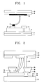
- Figure 1 is a sectional view showing the structure of a general FED device.
- a conventional FED device includes an upper glass substrate 10; an anode electrode 11 formed on the upper glass substrate 10; a phosphor layer 12 formed on the anode electrode 11; a lower glass substrate 1; a gate electrode 2 formed on the lower glass substrate 1; an insulation layer 3 formed on the gate electrode 2; a cathode electrode 5 formed on the insulation layer 3; a CNT (Carbon Nano Tube) 6 formed on the cathode electrode 5; and a counter electrode 4 electrically connected with the gate electrode 2 exposed through a via hole of the insulation layer 3 and formed on the same plane with the cathode electrode 5.
- the upper glass substrate 10 and the lower glass substrate 1 are disposed at the opposite side with a certain interval therebetween.
- a mesh electrode is additionally formed.
- Figure 2 is a sectional view of an FED device having a mesh electrode in accordance with the conventional art.
- the EED device having a mesh electrode includes: an upper glass substrate 110; an anode electrode 100 formed on the upper glass substrate 110; a lower glass substrate 15; a conductive layer 20 formed on the lower glass substrate 15; an insulation layer 30 formed on the conductive layer 20; a cathode electrode 40 formed on the insulation layer 30; a CNT 50 formed on or near the cathode electrode 40; a gate electrode 25 electrically connected with the conductive layer 20 exposed through a via hole of the insulation layer 30; and mesh electrodes 70 supported by structures 60 formed on the cathode electrode 40 and on the gate electrode 25.
- the upper glass substrate 110 and the lower glass substrate 15 are disposed with a spacer 80 therebetween at a certain interval in a facing manner.
- the structures 60 are made of glass, and the mesh electrodes 70 are formed on the structures 60.
- the mesh electrodes 70 are disposed at an upper side of the gate electrode 25 and the cathode electrode 40, thereby spreading and distortion of electron beams can be prevented.
- the mesh electrodes 70 shields electric field generated by the anode electrode 100 so that the high voltage applied to the anode electrode 100 cannot affect the gate electrode 25 and the cathode electrode 40.
- electrons emitted from the CNT 50 are accelerated by the voltage applied to the mesh electrodes 70 and proceed toward the mesh electrodes 70.
- electrons are accelerated by the anode electric field, and then, collide with the phosphor layer 90.
- the mesh electrodes 70 serve to concentrate electron beams into the cell.
- the insulation layer 30 with a dielectric component is positioned between the gate electrode 25 and the cathode electrode 40, electric charges are charged in the insulation layer 30, and as the electrons emitted from the CNT 50 collide with the mesh electrodes 70, electric charges are also charged not only in the mesh electrodes but also in the structures 60 supporting the mesh electrodes 70, causing a problem that electron beams are distorted, a leakage current is increased to increase power consumption.
- the FED device has the following problems.
- one object of the present invention is to provide an apparatus and method for driving a field effect display (FED) device capable of preventing distortion of electron beams by removing electric charges charged in the insulation layer of an FED device.
- FED field effect display
- Another object of the present invention is to provide an apparatus and method for driving a field effect display (FED) device capable of reducing a leakage current by removing electric charges charged in mesh electrodes and structures for supporting the mesh electrodes of the FED device and preventing cross talk (interference) between neighboring cells by preventing distortion of electron beams.
- FED field effect display
- a method for driving a field effect display (FED) device including: applying a voltage to a specific electrode of an FED device during a blanking time of a display frame of an FED.
- a method for driving a field effect display (FED) device including: applying a positive voltage to a data electrode of the FED device during a display time of a display frame of an FED; and applying a lower voltage than the positive voltage to the data electrode during a blanking time of the display frame.
- FED field effect display
- a method for driving a field effect display (FED) device including: applying a data pulse having a positive voltage to a data electrode of the FED device during a display time of the display frame of an FED and applying a scan pulse having a negative voltage in synchronization with the data pulse to a scan electrode of the FED device; and applying a lower pulse than the data pulse to the data electrode during a blanking time of the display frame.
- FED field effect display
- a method for driving a field effect display (FED) device including: applying a data pulse having a positive voltage to a data electrode of the FED device and a scan pulse having a negative voltage synchronized with the data pulse to the scan electrode of the FED device during a display time of a display frame of an FED; applying a negative pulse having a negative voltage to the data electrode during a blanking time of the display frame in order to remove electric charge charged in an insulation layer of the FED device; applying a positive voltage to a mesh electrode of the FED device during a display time; and applying a lower voltage than a ground voltage to the mesh electrode during the blanking time in order to remove electric charges charged at the mesh electrode and on a structure supporting the mesh electrode.
- the mesh electrode is positioned on structures formed on the data electrode and the scan electrode.
- an apparatus for driving a field effect display (FED) device including: a first driving unit for applying a voltage to a data electrode of the FED device during a blanking time of a display frame of an FED.
- FED field effect display
- an apparatus for driving a field effect display (FED) device including: a data driving unit for applying a data pulse having a positive voltage to a data electrode of an FED device during a display time of a display frame of an FED and applying a negative pulse having a negative voltage to a data electrode during a blanking time of the display frame; a scan driving unit for applying a scan pulse having a negative voltage synchronized with the data pulse to a scan electrode of the FED device; and a first driving unit for applying a voltage not higher than a ground voltage to a mesh electrode during the blanking time.
- the mesh electrode is positioned on structures formed on the data electrode and the scan electrode.
- An apparatus and method for driving an FED device capable of removing electric charges unnecessarily charged in the FED device by applying a voltage lower than a ground voltage to a specific electrode (i.e., a data electrode and a mesh electrode) of the FED device during a blanking time of a display frame of an FED in accordance with a preferred embodiment of the present invention will be described with reference to Figures 3 to 9.
- Figure 3 shows pulses applied to an FED device in accordance with a first embodiment of the present invention.
- a display unit of a screen As shown in Figure 3, as for a pulse applied based on a frame, a display unit of a screen, a vertical synchronizing signal, namely, one display frame (or frame frequency) includes a display time for displaying data on an FED and a blanking time for not displaying data.
- a scan pulse (-Vs) having a negative voltage is sequentially applied to scan electrodes (cathode electrode) (scan 1 - scan n), and simultaneously, a data pulse having a positive voltage in synchronization with the scan pulse is applied to a data electrode (gate electrode) according to a PWM (Pulse Width Modulation) method, thereby displaying data on the FED.
- a scan pulse (-Vs) having a negative voltage is sequentially applied to scan electrodes (cathode electrode) (scan 1 - scan n), and simultaneously, a data pulse having a positive voltage in synchronization with the scan pulse is applied to a data electrode (gate electrode) according to a PWM (Pulse Width Modulation) method, thereby displaying data on the FED.
- PWM Pulse Width Modulation
- a negative voltage (-Vr) is applied to the data electrode (gate electrode) during the blanking time in order to remove electric charges charged at the insulation layer of the FED device. Namely, by applying the negative voltage (-Vr) to the data electrode during the blanking time, electric charges charged in the insulation layer of the FED device can be removed, and thus, a flashover phenomenon generated due to the electric charges charged in the insulation layer would not occur.
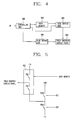
- Figure 4 is a block diagram showing a unit for driving the FED device in accordance with the first embodiment of the present invention.
- an apparatus for driving an FED device includes a controlling unit 200 for receiving a video signal and a synchronizing signal (IN), storing data with respect to the video signal in a data memory 300, and outputting a control signal (i.e., a horizontal/vertical synchronizing signal); a data driving unit 400 for receiving the control signal from the controller 200 and outputting a data pulse which has been pulse-width-modulated; and a scan driving unit 500 for receiving a control signal from the controller 200 and outputting a scan pulse in synchronization with the data pulse.
- An FED panel 600 receives the data pulse and the scan pulse and displays the video signal.
- the data driving unit 400 outputs a data pulse having a positive voltage (VD) to the data electrode during a display time for displaying the video signal and outputs a negative pulse having a negative voltage (-Vr) to the data electrode during a blanking time during a vertical synchronizing signal period under the control of the controller 200.
- VD positive voltage
- -Vr negative voltage
- the negative pulse having the negative voltage (-Vr) is applied to all the data electrodes (gate electrodes) of the FED panel 600 during the blanking time of the vertical synchronizing signal to remove electric charges charged in the insulation layer.
- Figure 5 is a detailed circuit diagram of a data driving unit of Figure 4, that is, a partial circuit of the data driving unit connected with one data electrode of the FED panel.
- the circuit of the data driving unit can be changed variably.
- the data driving unit 400 includes a plurality of switching units SWd1 and SWd2 for outputting the negative voltage (-Vr) or the ground voltage (GND) by control' signals SC1 and SC2 outputted from the controlling unit 200; and a data driving IC 410 including a plurality of switching units SD1 and SD2 outputting the positive voltage +V D or a voltage (ground voltage or -Vr) outputted by the switching units SWd1 and SWd2 to the data electrodes (gate electrodes) of the display panel 600 according to the control signals SC1 and SC2 outputted from the controlling unit 200.
- the plurality of switching units SWd1 and SWd2 determine polarity of a voltage applied to the data electrodes (gate electrodes) of the FED panel.
- the switch unit SD1 is turned off, the switching unit SWd1 is turned off, and then, the switching unit SWd2 is turned on.
- the data driving IC 410 outputs a negative pulse of a negative voltage to the data electrode.
- the switching unit SWd2 is turned on during the blanking time of the vertical synchronizing signal (or one frame) under the control of the controller 200 to output the negative pulse to the data electrode.
- the data driving unit can apply the positive pulse with the positive voltage to the data electrode of the FED panel during the display time for displaying data with respect to the video signal stored in the data memory and apply the negative pulse with the negative voltage to the data electrode during the blanking time, thereby removing electric charges charged in the insulation layer of the FED device.
- electric charges charged in the mesh electrode and in the structure supporting the mesh electrode can be removed by applying the ground voltage or the negative voltage to the mesh electrode (reference numeral 70 of Figure 2).
- Figure 6 shows a pulse for driving an FED in accordance with a second embodiment of the present invention.
- a scan pulse with a negative voltage is sequentially applied to the scan electrodes (cathode electrodes) (scan1 ⁇ scan n) during the display time and a data pulse with a positive voltage in synchronization with the scan pulse is applied to the data electrodes (gate electrodes), to display data on the FED.
- a positive voltage is applied to the mesh electrode during the display time.
- the ground voltage or the negative voltage i.e., -Vr
- the ground voltage or the negative voltage is applied to the mesh electrode during the blanking time. Namely, by applying a voltage not higher than the ground voltage to the mesh electrode during the blanking time, electric charges charged in the mesh electrode and the structure (made of glass) supporting the mesh electrode can be removed, and thus, a leakage current through the mesh electrode can be reduced.
- a current leaked through the mesh electrode can be reduced, the luminance of the FED can be enhanced, and distortion of electron beams and cross talk (interference) among the neighboring cells can be prevented.
- a high voltage can be applied to the FED device and thus the luminance of the FED can be enhanced.
- FIG. 7 is a block diagram of a driving unit for applying a pulse to a mesh electrode in accordance with the second embodiment of the present invention.
- the driving unit for applying the positive voltage (pulse) or the ground voltage to the mesh electrode can be changed variably and have various structures.
- the driving unit includes: a vertical synchronizing signal output unit 220 for outputting a vertical synchronizing signal according to a frame frequency; a monostable multivibrator 230 for generating a pulse in synchronization with the vertical synchronizing signal; an inverter/level converter 240 for inverting a signal of a pulse outputted from the monostable multivibrator 230, changing a level of the inverted signal, and outputting the level-changed signal as a switch drive signal; and a switching unit 250 for outputting a positive voltage (+Vs) according to the switch drive signal or outputting a ground voltage (or a negative voltage according to a structure of a circuit).
- a vertical synchronizing signal output unit 220 for outputting a vertical synchronizing signal according to a frame frequency
- a monostable multivibrator 230 for generating a pulse in synchronization with the vertical synchronizing signal
- an inverter/level converter 240 for inverting a signal of a pulse outputted
- the vertical synchronizing signal output unit 220 can output a used vertical synchronizing signal as it is in order to output a video signal, or can obtain a vertical synchronizing signal from a processor (not shown) for providing the video signal.
- An oscillator 210 for oscillating a signal corresponding to the vertical synchronizing signal can be used instead of the vertical synchronizing signal output unit 220.
- Figure 8 shows waveforms of an output signal applied to the mesh electrode from the driving unit of Figure 7 and of operation signals of switching units for generating the output signal.
- a voltage applied to the mesh electrode can be provided in a pulse form according to the frame frequency, and while a first signal is applied to a first switch SWd of the switch unit 250, a positive voltage is applied to the mesh electrode, and while a second signal is applied to the second switch SWe, the ground voltage is applied to the mesh electrode.
- Figure 9 shows a difference between a current leaked when a pulse is applied to the mesh electrode in accordance with the second embodiment of the present invention and a current leaked through a mesh electrode when a DC voltage is applied to the mesh electrode in accordance with the conventional art.
- the mesh electrode driving method of the present invention can considerably reduce the leakage current compared with the conventional art.
- the mesh electrode driving method of the present invention can considerably reduce the mesh leakage current compared to the conventional art.
- a voltage lower than the voltage applied to the data electrode and/or the mesh electrode of the FED device during the display time of the display frame of the FED is applied to the data electrode and/or the mesh electrode during the blanking time of the display frame of the FED, whereby the electric charges charged in the insulation layer of the FED device can be removed and also the electric charges charged in the mesh electrode and the structure supporting the mesh electrode can be removed.
- the method for driving the FED device of the present invention has many advantages.
Landscapes
- Engineering & Computer Science (AREA)
- Physics & Mathematics (AREA)
- Computer Hardware Design (AREA)
- General Physics & Mathematics (AREA)
- Theoretical Computer Science (AREA)
- Control Of Indicators Other Than Cathode Ray Tubes (AREA)
Applications Claiming Priority (4)
| Application Number | Priority Date | Filing Date | Title |
|---|---|---|---|
| KR1020040015142A KR20050089640A (ko) | 2004-03-05 | 2004-03-05 | 탄소 나노튜브 전계방출소자 구동 방법 |
| KR2004015142 | 2004-03-05 | ||
| KR2004016632 | 2004-03-11 | ||
| KR1020040016632A KR20050091282A (ko) | 2004-03-11 | 2004-03-11 | 탄소 나노 튜브 전계 방출 소자 구동 방법 |
Publications (2)
| Publication Number | Publication Date |
|---|---|
| EP1577866A2 true EP1577866A2 (de) | 2005-09-21 |
| EP1577866A3 EP1577866A3 (de) | 2007-07-11 |
Family
ID=34840295
Family Applications (1)
| Application Number | Title | Priority Date | Filing Date |
|---|---|---|---|
| EP05290471A Withdrawn EP1577866A3 (de) | 2004-03-05 | 2005-03-02 | Gerät und Verfahren zur Ansteuerung einer Feldemissionanzeigevorrichtung |
Country Status (2)
| Country | Link |
|---|---|
| US (1) | US7280089B2 (de) |
| EP (1) | EP1577866A3 (de) |
Cited By (1)
| Publication number | Priority date | Publication date | Assignee | Title |
|---|---|---|---|---|
| CN106782289A (zh) * | 2017-02-02 | 2017-05-31 | 友达光电股份有限公司 | 显示面板及其控制方法 |
Families Citing this family (4)
| Publication number | Priority date | Publication date | Assignee | Title |
|---|---|---|---|---|
| KR101022658B1 (ko) * | 2004-05-31 | 2011-03-22 | 삼성에스디아이 주식회사 | 신호 지연 저감형 전자 방출 장치 구동방법 |
| US7393699B2 (en) | 2006-06-12 | 2008-07-01 | Tran Bao Q | NANO-electronics |
| TWI416450B (zh) * | 2009-09-09 | 2013-11-21 | Tatung Co | 場發射顯示面板的驅動電路和方法及場發射顯示器 |
| US10135333B1 (en) * | 2013-10-04 | 2018-11-20 | Silego Technology, Inc. | Enhanced conduction for p-channel device |
Family Cites Families (11)
| Publication number | Priority date | Publication date | Assignee | Title |
|---|---|---|---|---|
| US5594305A (en) * | 1995-06-07 | 1997-01-14 | Texas Instruments Incorporated | Power supply for use with switched anode field emission display including energy recovery apparatus |
| US5578900A (en) * | 1995-11-01 | 1996-11-26 | Industrial Technology Research Institute | Built in ion pump for field emission display |
| JP2000020019A (ja) * | 1998-06-30 | 2000-01-21 | Toshiba Corp | 電界放出型表示装置 |
| US6133893A (en) * | 1998-08-31 | 2000-10-17 | Candescent Technologies, Inc. | System and method for improving emitter life in flat panel field emission displays |
| US6617798B2 (en) * | 2000-03-23 | 2003-09-09 | Samsung Sdi Co., Ltd. | Flat panel display device having planar field emission source |
| US6882330B2 (en) * | 2001-03-26 | 2005-04-19 | Lg Electronics Inc. | Field emission displaying device and driving method thereof |
| TW502282B (en) * | 2001-06-01 | 2002-09-11 | Delta Optoelectronics Inc | Manufacture method of emitter of field emission display |
| KR100470207B1 (ko) * | 2001-08-13 | 2005-02-04 | 엘지전자 주식회사 | 평면 전계방출 표시소자의 구동장치 및 방법 |
| JP4211323B2 (ja) * | 2002-02-27 | 2009-01-21 | 株式会社日立製作所 | 画像表示装置およびその駆動方法 |
| US6646282B1 (en) * | 2002-07-12 | 2003-11-11 | Hon Hai Precision Ind. Co., Ltd. | Field emission display device |
| US20040155839A1 (en) * | 2003-01-27 | 2004-08-12 | Lg Electronics Inc. | Scan driving apparatus and method of field emission display device |
-
2005
- 2005-03-02 EP EP05290471A patent/EP1577866A3/de not_active Withdrawn
- 2005-03-03 US US11/069,944 patent/US7280089B2/en not_active Expired - Fee Related
Cited By (1)
| Publication number | Priority date | Publication date | Assignee | Title |
|---|---|---|---|---|
| CN106782289A (zh) * | 2017-02-02 | 2017-05-31 | 友达光电股份有限公司 | 显示面板及其控制方法 |
Also Published As
| Publication number | Publication date |
|---|---|
| US7280089B2 (en) | 2007-10-09 |
| EP1577866A3 (de) | 2007-07-11 |
| US20050194911A1 (en) | 2005-09-08 |
Similar Documents
| Publication | Publication Date | Title |
|---|---|---|
| KR20050032321A (ko) | 전계방출표시장치 및 그 구동방법 | |
| US7280089B2 (en) | Apparatus and method for driving field emission display device | |
| US20040155839A1 (en) | Scan driving apparatus and method of field emission display device | |
| US20050184644A1 (en) | Field emission display device | |
| EP1571690A1 (de) | Feldemissionsanzeigevorrichtung | |
| US20020175906A1 (en) | Flat panel display and driving method thereof | |
| US7138761B2 (en) | Field emission display and driving method thereof | |
| KR100444504B1 (ko) | 전계 방출 표시소자 | |
| KR20030008692A (ko) | 평면 전계방출 표시소자의 구동장치 및 방법 | |
| US7221336B2 (en) | Aging driving apparatus of field emission display device and driving method | |
| KR100329777B1 (ko) | 어드레스 구간에서의 플라즈마 디스플레이 패널 구동 방법 | |
| KR20060037882A (ko) | 평판 표시장치용 휘도조절장치 및 이의 휘도조절방법 | |
| KR100664028B1 (ko) | 전계 방출 표시 패널 및 그 구동 방법 | |
| KR100318064B1 (ko) | 고주파구동 전계 방출 표시장치 및 그 구동방법 | |
| US20030030600A1 (en) | Apparatus for driving metal insulator metal field emission display device and method for same | |
| KR100415614B1 (ko) | 액티브 형 평면 전계방출 표시소자 및 그 구동방법 | |
| US7358933B2 (en) | Electron emission display and driving method thereof | |
| KR20050091282A (ko) | 탄소 나노 튜브 전계 방출 소자 구동 방법 | |
| KR20050089640A (ko) | 탄소 나노튜브 전계방출소자 구동 방법 | |
| KR100585633B1 (ko) | 고주파용 플라즈마 표시장치의 구동방법 | |
| KR100556479B1 (ko) | 고주파용 플라즈마 표시장치 | |
| US20050095947A1 (en) | Field emission display device and driving method thereof | |
| CN1216398C (zh) | 低调制电压动态范围的场发射门电极和调制电极的组件 | |
| US20040207576A1 (en) | Spacer discharging apparatus and method of field emission display | |
| EP1708156A2 (de) | Verfahren und Vorrichtung zur Ansteuerung einer Elektronenemissionstafel |
Legal Events
| Date | Code | Title | Description |
|---|---|---|---|
| PUAI | Public reference made under article 153(3) epc to a published international application that has entered the european phase |
Free format text: ORIGINAL CODE: 0009012 |
|
| AK | Designated contracting states |
Kind code of ref document: A2 Designated state(s): AT BE BG CH CY CZ DE DK EE ES FI FR GB GR HU IE IS IT LI LT LU MC NL PL PT RO SE SI SK TR |
|
| AX | Request for extension of the european patent |
Extension state: AL BA HR LV MK YU |
|
| PUAL | Search report despatched |
Free format text: ORIGINAL CODE: 0009013 |
|
| AK | Designated contracting states |
Kind code of ref document: A3 Designated state(s): AT BE BG CH CY CZ DE DK EE ES FI FR GB GR HU IE IS IT LI LT LU MC NL PL PT RO SE SI SK TR |
|
| AX | Request for extension of the european patent |
Extension state: AL BA HR LV MK YU |
|
| 17P | Request for examination filed |
Effective date: 20080115 |
|
| AKX | Designation fees paid |
Designated state(s): DE DK FR |
|
| STAA | Information on the status of an ep patent application or granted ep patent |
Free format text: STATUS: THE APPLICATION HAS BEEN WITHDRAWN |
|
| 18W | Application withdrawn |
Effective date: 20080626 |