EP1577862A1 - Display and electronic device - Google Patents
Display and electronic device Download PDFInfo
- Publication number
- EP1577862A1 EP1577862A1 EP03780766A EP03780766A EP1577862A1 EP 1577862 A1 EP1577862 A1 EP 1577862A1 EP 03780766 A EP03780766 A EP 03780766A EP 03780766 A EP03780766 A EP 03780766A EP 1577862 A1 EP1577862 A1 EP 1577862A1
- Authority
- EP
- European Patent Office
- Prior art keywords
- display
- display screen
- housing
- display device
- dual
- Prior art date
- Legal status (The legal status is an assumption and is not a legal conclusion. Google has not performed a legal analysis and makes no representation as to the accuracy of the status listed.)
- Granted
Links
Images




Classifications
-
- H—ELECTRICITY
- H05—ELECTRIC TECHNIQUES NOT OTHERWISE PROVIDED FOR
- H05B—ELECTRIC HEATING; ELECTRIC LIGHT SOURCES NOT OTHERWISE PROVIDED FOR; CIRCUIT ARRANGEMENTS FOR ELECTRIC LIGHT SOURCES, IN GENERAL
- H05B33/00—Electroluminescent light sources
-
- H—ELECTRICITY
- H04—ELECTRIC COMMUNICATION TECHNIQUE
- H04M—TELEPHONIC COMMUNICATION
- H04M1/00—Substation equipment, e.g. for use by subscribers
- H04M1/02—Constructional features of telephone sets
- H04M1/0202—Portable telephone sets, e.g. cordless phones, mobile phones or bar type handsets
- H04M1/0206—Portable telephones comprising a plurality of mechanically joined movable body parts, e.g. hinged housings
- H04M1/0247—Portable telephones comprising a plurality of mechanically joined movable body parts, e.g. hinged housings comprising more than two body parts
-
- G—PHYSICS
- G06—COMPUTING OR CALCULATING; COUNTING
- G06F—ELECTRIC DIGITAL DATA PROCESSING
- G06F1/00—Details not covered by groups G06F3/00 - G06F13/00 and G06F21/00
-
- G—PHYSICS
- G06—COMPUTING OR CALCULATING; COUNTING
- G06F—ELECTRIC DIGITAL DATA PROCESSING
- G06F1/00—Details not covered by groups G06F3/00 - G06F13/00 and G06F21/00
- G06F1/16—Constructional details or arrangements
- G06F1/1613—Constructional details or arrangements for portable computers
- G06F1/1615—Constructional details or arrangements for portable computers with several enclosures having relative motions, each enclosure supporting at least one I/O or computing function
- G06F1/1616—Constructional details or arrangements for portable computers with several enclosures having relative motions, each enclosure supporting at least one I/O or computing function with folding flat displays, e.g. laptop computers or notebooks having a clamshell configuration, with body parts pivoting to an open position around an axis parallel to the plane they define in closed position
-
- G—PHYSICS
- G06—COMPUTING OR CALCULATING; COUNTING
- G06F—ELECTRIC DIGITAL DATA PROCESSING
- G06F1/00—Details not covered by groups G06F3/00 - G06F13/00 and G06F21/00
- G06F1/16—Constructional details or arrangements
- G06F1/1613—Constructional details or arrangements for portable computers
- G06F1/1633—Constructional details or arrangements of portable computers not specific to the type of enclosures covered by groups G06F1/1615 - G06F1/1626
- G06F1/1637—Details related to the display arrangement, including those related to the mounting of the display in the housing
-
- G—PHYSICS
- G06—COMPUTING OR CALCULATING; COUNTING
- G06F—ELECTRIC DIGITAL DATA PROCESSING
- G06F1/00—Details not covered by groups G06F3/00 - G06F13/00 and G06F21/00
- G06F1/16—Constructional details or arrangements
- G06F1/1613—Constructional details or arrangements for portable computers
- G06F1/1633—Constructional details or arrangements of portable computers not specific to the type of enclosures covered by groups G06F1/1615 - G06F1/1626
- G06F1/1637—Details related to the display arrangement, including those related to the mounting of the display in the housing
- G06F1/1647—Details related to the display arrangement, including those related to the mounting of the display in the housing including at least an additional display
-
- G—PHYSICS
- G06—COMPUTING OR CALCULATING; COUNTING
- G06F—ELECTRIC DIGITAL DATA PROCESSING
- G06F1/00—Details not covered by groups G06F3/00 - G06F13/00 and G06F21/00
- G06F1/16—Constructional details or arrangements
- G06F1/1613—Constructional details or arrangements for portable computers
- G06F1/1633—Constructional details or arrangements of portable computers not specific to the type of enclosures covered by groups G06F1/1615 - G06F1/1626
- G06F1/1637—Details related to the display arrangement, including those related to the mounting of the display in the housing
- G06F1/1652—Details related to the display arrangement, including those related to the mounting of the display in the housing the display being flexible, e.g. mimicking a sheet of paper, or rollable
-
- G—PHYSICS
- G06—COMPUTING OR CALCULATING; COUNTING
- G06F—ELECTRIC DIGITAL DATA PROCESSING
- G06F3/00—Input arrangements for transferring data to be processed into a form capable of being handled by the computer; Output arrangements for transferring data from processing unit to output unit, e.g. interface arrangements
- G06F3/14—Digital output to display device ; Cooperation and interconnection of the display device with other functional units
- G06F3/1423—Digital output to display device ; Cooperation and interconnection of the display device with other functional units controlling a plurality of local displays, e.g. CRT and flat panel display
-
- G—PHYSICS
- G09—EDUCATION; CRYPTOGRAPHY; DISPLAY; ADVERTISING; SEALS
- G09F—DISPLAYING; ADVERTISING; SIGNS; LABELS OR NAME-PLATES; SEALS
- G09F9/00—Indicating arrangements for variable information in which the information is built-up on a support by selection or combination of individual elements
- G09F9/30—Indicating arrangements for variable information in which the information is built-up on a support by selection or combination of individual elements in which the desired character or characters are formed by combining individual elements
-
- H—ELECTRICITY
- H05—ELECTRIC TECHNIQUES NOT OTHERWISE PROVIDED FOR
- H05B—ELECTRIC HEATING; ELECTRIC LIGHT SOURCES NOT OTHERWISE PROVIDED FOR; CIRCUIT ARRANGEMENTS FOR ELECTRIC LIGHT SOURCES, IN GENERAL
- H05B33/00—Electroluminescent light sources
- H05B33/12—Light sources with substantially two-dimensional [2D] radiating surfaces
- H05B33/14—Light sources with substantially two-dimensional [2D] radiating surfaces characterised by the chemical or physical composition or the arrangement of the electroluminescent material, or by the simultaneous addition of the electroluminescent material in or onto the light source
-
- H—ELECTRICITY
- H04—ELECTRIC COMMUNICATION TECHNIQUE
- H04M—TELEPHONIC COMMUNICATION
- H04M1/00—Substation equipment, e.g. for use by subscribers
- H04M1/02—Constructional features of telephone sets
- H04M1/0202—Portable telephone sets, e.g. cordless phones, mobile phones or bar type handsets
- H04M1/0206—Portable telephones comprising a plurality of mechanically joined movable body parts, e.g. hinged housings
- H04M1/0208—Portable telephones comprising a plurality of mechanically joined movable body parts, e.g. hinged housings characterized by the relative motions of the body parts
- H04M1/0214—Foldable telephones, i.e. with body parts pivoting to an open position around an axis parallel to the plane they define in closed position
-
- H—ELECTRICITY
- H04—ELECTRIC COMMUNICATION TECHNIQUE
- H04M—TELEPHONIC COMMUNICATION
- H04M1/00—Substation equipment, e.g. for use by subscribers
- H04M1/02—Constructional features of telephone sets
- H04M1/0202—Portable telephone sets, e.g. cordless phones, mobile phones or bar type handsets
- H04M1/026—Details of the structure or mounting of specific components
- H04M1/0266—Details of the structure or mounting of specific components for a display module assembly
-
- H—ELECTRICITY
- H04—ELECTRIC COMMUNICATION TECHNIQUE
- H04M—TELEPHONIC COMMUNICATION
- H04M2250/00—Details of telephonic subscriber devices
- H04M2250/16—Details of telephonic subscriber devices including more than one display unit
Definitions
- the present invention relates to a display device having a light emitting element, and more particularly relates to a portable information terminal such as a mobile phone and a PDA (Personal Digital Assistant).
- a portable information terminal such as a mobile phone and a PDA (Personal Digital Assistant).
- a display device using a self-light emitting element typified by an electro-luminescence (EL) element and the like has been studied and developed instead of a liquid crystal display (LCD) using a liquid crystal element for a pixel.
- EL electro-luminescence
- Such a light emitting device has the advantages of high image quality and wide viewing angle because of a light emitting type, and reduced thickness and weight and the like without need of a back light.
- the light emitting device is expected to be widely used for a display screen of a mobile phone and a display device.
- a portable information terminal As for a portable information terminal, a high added value is required with diversification of uses. Recently, a display can be used not only for displaying calls and e-mails but also for displaying landscapes, persons and the like with camera function and browsing Web pages. Further, applications have been enriched. In the future, a portable information terminal having a function to display images of a film, television and the like is expected to be widely used.
- a display of a display device particularly that of a portable information terminal has become to display more amount of information.
- an existing display has a small screen which is seen with difficulty, therefore, spectacular images are not displayed easily.
- a display device and a portable information terminal each provided with a larger display are needed.
- the display device and the portable information terminal are required to be reduced in weight, thickness and size, which trades off between a high added value.
- a display device and a portable information terminal each including a dual light emission panel (a panel capable of displaying on both screens) and being capable of realizing a module with a small volume.
- the invention will take the following measures.
- a display device comprises a first display screen, a first housing and a second housing that are connected to each other, and a dual light emission panel (hereinafter referred to as a dual display panel) that includes a second display screen on the front side and a third display screen on the back side.
- the dual display panel is connected to the first housing, disposed between the first housing and the second housing when overlapping the first housing, and rotated around a connecting point of the dual display panel and the first housing.
- the first housing and the second housing can overlap with the dual display panel interposed therebetween.
- a display device comprises a display screen including a plurality of pixels arranged in matrix.
- the display device comprises a plurality of panels at least one of which is a dual display panel including a display screen each on the front side and the back side.
- the display device of the invention comprises a second display screen as a display screen on one side of the front side and the back side of the dual display panel, a third display screen as a display screen on the other side, and a first display screen as a display screen other than the second display screen and the third display screen.
- the display device has a first display state in which the second display screen is used, and a second display state in which the first display screen and the third display screen are used.
- one image in the second display state, one image may be divided into two images one of which is a first image and the other is a second image, and the first image may be displayed on one of the first display screen and the third display screen and the second image may be displayed on the other screen.
- the first display screen and the third display screen can display different images.
- the display device can be applied to a portable information terminal.
- the dual display panel may use an EL element as a display element.
- the display device may be a foldable type.
- the dual display panel can constitute a display device having a flat surface or a curved surface.
- a display with a larger screen can be mounted in a display device and a portable information terminal that have been limited in screen size.
- a display device itself can be formed thinner than that using two single display panels. Therefore, a higher added value of a display device and a portable information terminal can be realized while reducing the weight, thickness and size thereof.
- FIG 1 shows an example of a flip phone including a dual display panel 1003.
- the flip phone comprises a first housing 1001, a second housing 1002 and a dual display panel 1003.
- the first housing 1001 includes an audio output portion 1004, a first display screen 1005 and the like
- the second housing 1002 includes an operating button 1006, an audio input portion 1007 and the like.
- the dual display panel 1003 includes a second display screen 1008, a third display screen 1101 and the like.
- the dual display panel 1003 is disposed between the first housing 1001 and the second housing 1002 of the mobile phone.
- the second display screen 1008 of the dual display panel 1003 namely, only a single display screen is used.
- the third display screen 1101 of the dual display panel 1003 and the first display screen 1005, namely, two display screens can be used.
- FIG. 2A shows an example of a first display state in which images are displayed on a single screen.
- a second display screen 2001 is used for displaying a relatively small amount of information such as calls and e-mails or displaying in a low power consumption mode.
- FIG. 2B shows an example of a second display state in which images are displayed on two screens.
- the second display state in which images are displayed on a third display screen 2101 and a first display screen 2102 is used for displaying a film or television on a larger screen or magnifying and displaying images of the second display screen 2001. That is, one image is divided into two images one of which is displayed on the third display screen 2101 and the other of which is displayed on the first display screen 2102. Operations of the screens in the second display state may be carried out with a side operating button 2103, or with the third display screen 2101 or the first display screen 2102 that is made to be used as a touch panel.
- different images may be displayed on the third display screen 2101 and the first display screen 2102.
- an image of a person called is displayed on one screen while a Web page, an address book and the like are displayed on the other screen, or an image of a person called is displayed on one screen while the user's own image is displayed on the other screen.
- images of the persons called may be displayed separately.
- FIG 5 shows an example in which a dual display panel is rotated around the right side of a first display screen 5001 of a mobile phone, and images are displayed on two screens of the first display screen 5001 and a third display screen 5002.
- a connecting point of the first display screen and the dual display panel 1003 of a mobile phone may be arranged anywhere around the first housing.
- a dual display panel is used for a mobile phone in this embodiment mode, it may be used for a portable information terminal such as a PDA and a laptop personal computer. Further, the dual display panel may be formed of plastic or glass. Alternatively, it may be a foldable film panel. According to this, the dual display panel has a curved surface as well as a flat surface.
- a dual light emission panel having a first display screen and a second display screen is described.
- a pixel electrode or a counter electrode using a light transmitting material means a transparent conductive film such as ITO or a film using aluminum and the like formed with a thickness that allows light to transmit through it, and a reflective material means a conductive material using aluminum and the like, which reflects light.
- FIG 6A comprises a driving TFT 6001, a pixel electrode 6002 using a light transmitting material, an EL layer 6003, a counter electrode 6004 using a light transmitting material, a first display area 6005, a second display area 6006 and the like.
- the pixel electrode 6002 and the counter electrode 6004 use a light transmitting material, light from the EL layer 6003 is emitted in both directions of the counter electrode 6004 and the pixel electrode 6002.
- FIG 6B comprises a first driving TFT 6101, a second driving TFT 6102, a first pixel electrode 6103 using a reflective material, a second pixel electrode 6104 using a light transmitting material, an EL layer 6105, a counter electrode 6106 using a light transmitting material, a reflective film 6107 using a reflective material, a first display area 6108, a second display area 6109 and the like.
- the first pixel electrode 6103 reflects light and the counter electrode 6106 transmits light, light from the EL layer 6105 is emitted in the direction of the counter electrode 6106.
- a current flows between the second pixel electrode 6104 connected to the second driving TFT 6102 and the counter electrode 6106, and thereby the EL layer 6105 in the second display area 6109 emits light.
- the reflective film 6107 reflects light and the second pixel electrode 6104 transmits light, light from the EL layer 6105 is emitted in the direction of the pixel electrode 6104.
- the emission color of the EL layer may be either mono-color or RGB full color, and a color filter may also be combined therewith.
- the full color emission may be achieved by a white EL layer with color filters.
- the EL layer 6105 is formed of an organic compound or a charge injection transporting substance that contains an inorganic compound, and a light emitting material.
- the EL layer 6105 includes a layer of one or plural kinds selected from the group consisting of a low molecular weight organic compound, a medium molecular weight organic compound (that does not have subliming property and that has a molecularity of 20 or less, or a length of chained molecules of 10 ⁇ m or less), and a high molecular weight organic compound, which are relative to molecularity.
- the EL layer 6105 may include a layer that is formed of the organic compound combined with an inorganic compound with electron injection transporting property or hole injection transporting property.
- the charge injection transporting substance as an inorganic compound material includes diamond-like carbon (DLC), Si, Ge, and oxide or nitride of these substances, and may be appropriately doped with P, B, N or the like. Further, the charge injection transporting substance may include an oxide, a nitride, or a fluoride of alkali metal or alkali earth metal, and a compound or an alloy of the metal and Zn, Sn, V, Ru, Sm, or In.
- DLC diamond-like carbon
- Si silicon
- Ge silicon
- oxide or nitride of these substances and may be appropriately doped with P, B, N or the like.
- the charge injection transporting substance may include an oxide, a nitride, or a fluoride of alkali metal or alkali earth metal, and a compound or an alloy of the metal and Zn, Sn, V, Ru, Sm, or In.
- a low molecular weight organic light emitting material as a preferable material forming the EL layer 6105 includes Alq 3 , BAlq 2 , Almq 3 , DPVBi, PVK, a triphenylamine derivative (TPD), and the like. These materials are used as host materials, and quinacridone or the like is added as a dopant.
- a high molecular weight organic light emitting material is physically stronger than a low molecular weight material and superior in durability of the element. Furthermore, a high molecular weight material can be formed by an application method and therefore manufacture of the element is relatively easy.
- the structure of a light emitting element using a high molecular weight organic light emitting material is basically the same as that of a light emitting element using a low molecular weight organic light emitting material, and has a cathode / an organic light emitting layer / an anode.
- the EL layer 6105 is formed from a high molecular weight organic light emitting material
- a two-layer structure is employed in many cases. This is because it is difficult to form a laminated structure using a high molecular weight material unlike the case of using a low molecular weight organic light emitting material.
- the EL layer using a high molecular weight organic light emitting material has a cathode / a light emitting layer / a hole transporting layer / an anode. The emission color is determined by the material of its light emitting layer. Therefore, a light emitting element that emits light of desired color can be formed by selecting an appropriate material of the light emitting layer.
- the high molecular weight electro luminescent material that can be used to form a light emitting layer is a polyparaphenylene vinylene-based material, a polyparaphenylene-based material, a polythiophen-based material, or a polyfluorene-based material.
- the polyparaphenylene vinylene-based material is a derivative of poly (paraphenylene vinylene) [PPV], for example, poly (2, 5-dialkoxy-1, 4-phenylene vinylene) [RO-PPV], poly (2-(2'-ethyl-hexoxy)-5-metoxy-1, 4-phenylene vinylene) [MEH-PPV], poly (2-(dialkoxyphenyl)-1, 4-phenylene vinylene) [ROPh-PPV], and the like.
- poly (paraphenylene vinylene) [PPV] poly (2, 5-dialkoxy-1, 4-phenylene vinylene) [RO-PPV]
- the polyparaphenylene-based material is a derivative of polyparaphenylene [PPP], for example, poly (2, 5-dialkoxy-1, 4-phenylene) [RO-PPP], poly (2, 5-dihexoxy-1, 4-phenylene), and the like.
- the polythiophene-based material is a derivative of polythiophene [PT], for example, poly (3-alkylthiophene) [PAT], poly (3-hexylthiophene) [PHT], poly (3-cyclohexylthiophene) [PCHT], poly (3-cyclohexyl-4-methilthiophene) [PCHMT], poly (3, 4-dicyclohexylthiophene) [PDCHT], poly [3-(4-octylphenyl)-thiophene] [POPT], poly [3-(4-octylphenyl)-2, 2 bithiophene] [PTOPT], and the like.
- PT poly (3-alkylthiophene) [PAT]
- PHT poly (3-hexylthiophene) [PHT]
- PCHT poly (3-cyclohexylthiophene) [PCHT]
- PCHMT poly (3-cyclohexyl
- the polyfluorene-based material is a derivative of polyfluorene [PF], for example, poly (9, 9-dialkylfluorene) [PDAF], poly (9, 9-dioctylfluorene) [PDOF], and the like.
- PF polyfluorene
- PDAF poly (9, 9-dialkylfluorene)
- PDOF poly (9, 9-dioctylfluorene)
- a light emitting element can be formed by arbitrarily laminating functional layers using these materials, such as a hole injection transporting layer, a hole transporting layer, an electron injection transporting layer, an electron transporting layer, a light emitting layer, an electron blocking layer, and a hole blocking layer. Further, a mixed layer or a mixed junction may be formed by combining these layers.
- an EL layer that emits white light for instance, Alq 3 , Alq 3 partially doped with Nile red that is a red light emitting pigment, Alq 3 , p-EtTAZ, and TPD (aromatic diamine) are layered in this order by a vapor deposition method to obtain white light.
- the layer after application is preferably baked by vacuum heating.
- an aqueous solution of poly (ethylene dioxythiophene) / poly (styrene sulfonic acid) (PEDOT / PSS) is applied to the entire surface and baked to form a film that functions as a hole injection layer.
- PVK polyvinyl carbazole
- a luminescence center pigment such as 1, 1, 4, 4-tetraphenyl-1, 3-butadiene (TPB), 4-dicyanomethylene-2-methyl-6-(p-dimethylamino-styryl)-4H-pyran (DCM1), Nile red, or coumarin 6
- TPB 1, 1, 4, 4-tetraphenyl-1, 3-butadiene
- DCM1 4-dicyanomethylene-2-methyl-6-(p-dimethylamino-styryl)-4H-pyran
- Nile red or coumarin 6
- the EL layer 6105 may be formed of a single layer.
- 1, 3, 4-oxadiazole derivative (PBD) capable of transporting electrons is dispersed in polyvinyl carbazole (PVK) capable of transporting holes.
- PVK polyvinyl carbazole
- Another method to obtain white light emission is to disperse 30 wt% of PBD as an electron transporting agent and disperse four kinds of pigments (TPB, coumarin 6, DCM1, and Nile red) in appropriate amounts.
- TPB trifluoride
- coumarin 6, DCM1, and Nile red pigments
- Other than the light emitting element shown here that provides white light emission by selecting materials of the EL layer 6105 arbitrarily, a light emitting element that provides red light emission, green light emission or blue light emission can be manufactured.
- a triplet exciton material containing a metal complex or the like may be used as well as the singlet exciton light emitting material described above.
- a signal control circuit 3001 comprises a CPU 3002, a memory A 3003, a memory B 3004, a memory controller 3005 and the like.
- a dual display panel 3007 comprises a first source signal line driver circuit 3008, a first gate signal line driver circuit 3009, a first display screen 3010, a second display screen that is on the back side of the first display screen, and the like.
- a display panel 3011 comprises a second source signal line driver circuit 3012, a second gate signal line driver circuit 3013, a third display screen 3014 and the like.
- a switch 3015 In a first display state, a switch 3015 is turned off. A signal and a driving voltage for operating the dual display panel 3007 are inputted from a display controller 3006 to the first source signal line driver circuit 3008, the first gate signal line driver circuit 3009 and the like. Since the switch 3015 is off at this time, the display panel 3011 does not operate.
- An image signal inputted to the signal control circuit 3001 is controlled by the memory controller 3005 to be inputted to the memory A 3003 or the memory B 3004 and stored therein. Then, the dual display panel 3007 is selected by the memory controller 3005, and the image signal that is sequentially read out from the memory A 3003 or the memory B 3004 is inputted to the first source signal line driver circuit 3008.
- the switch 3015 In a second display state, the switch 3015 is turned on. Since the switch 3015 is on, a signal and a driving voltage for operating the dual display panel 3007 and the display panel 3011 are inputted to the first source signal line driver circuit 3008, the first gate signal line driver circuit 3009, the second source signal line driver circuit 3012, the second gate signal line driver circuit 3013 and the like.
- an image signal is converted by the memory controller 3005 in accordance with the number of pixels and a display mode, and divided into left and right parts to be inputted to the dual display panel 3007 and the display panel 3008, respectively.
- a first image signal and a second image signal that have been inputted to the signal line control circuit 3001 are inputted to the memory A 3003 and the memory B 3004, respectively, and stored therein. Then, the first image signal is sequentially read out by the memory controller 3005 and inputted to the first source signal line driver circuit 3008, and the second image signal is inputted to the second source signal line driver circuit 3012.
- the configurations of the driver circuits in the dual display panel 3007 and the display panel 3011 are not limited to the general ones shown in this embodiment.
- the dual display panel 3007 may adopt a driver circuit configuration capable of being switched vertically to horizontally.
- Image signals stored in the memory A 3003 and the memory B 3004 may be rearranged by the memory 3005 depending on the display direction and displayed on the dual display panel 3007.
- the source signal line driver circuit and the gate signal line driver circuit may adopt a configuration capable of switching the scan direction in order to change vertically and horizontally or upwards and downwards depending on the display direction.
- a passive matrix type dual display panel may be adopted as well.
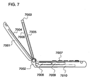
- FIG 7 shows an example of a cross sectional view of the display module explained in Embodiment 1.
- the display module in FIG. 7 comprises a first housing 7001, a second housing 7002 and a dual display panel 7003.
- the first housing 7001 includes a first display portion 7004 and the like
- the second housing 7002 includes an operating button 7007, a display controller 7008, a signal control portion 7009, a battery portion 7010 and the like
- the dual display panel 7003 includes a second display screen 7005, a third display screen 7006 and the like.
- the connection and operation of each part are similar to those shown in Embodiment 1.
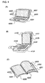
- Described herein is an example of the display device of the invention applied to a laptop personal computer, a PDA and an electronic book. Since one dual display panel can display images in both directions, the thickness of a housing of a display device can be reduced even in the case of, as shown in FIGS. 4A, 4B and 4C, display screens being provided on both sides of a panel.
- FIG 4A shows an example of a laptop personal computer mounting a dual display panel 4003.
- a first housing 4005 includes a first display screen 4001, a second housing 4006 includes an operating button 4004 and the like, and the dual display panel 4003 includes a second display screen 4002 on the front side and a third display screen on the back side of the second display screen 4002.
- the dual display panel 4003 is disposed between the first housing 4005 and the second housing 4006.
- the dual display panel 4003 overlaps the first housing, and the second display screen is used.
- the dual display panel overlaps the second housing and images are displayed on two screens.
- FIG. 4B shows an example of a PDA mounting a dual display panel 4103.
- a first housing 4105 includes a first display screen 4101
- a second housing 4106 includes an operating button 4104 and the like
- the dual display panel 4103 includes a second display screen 4102 on the front side and a third display screen on the back side of the second display screen 4102.
- the dual display panel 4103 is disposed between the first housing 4105 and the second housing 4106.
- the dual display panel 4103 overlaps the first housing, and the second display screen is used.
- the dual display panel overlaps the second housing and images are displayed on two screens.
- FIG 4C shows an example of an electronic book mounting a dual display panel 4203.
- a first housing 4205 includes a first display screen 4201
- a second housing 4206 includes an operating button 4204 and a fourth display screen 4207
- the dual display panel 4203 includes a second display screen 4202 on the front side and a third display screen on the back side.
- the dual display panel 4203 is disposed between the first housing and the second housing.
- the electronic book including the dual display panel 4203 it is usable to read texts on the first display screen 4201 and the third display screen while referring to drawings on the second display screen 4202 and the fourth display screen 4207.
- the display of the dual display panel may be changed from the third display screen to the second display screen.
- the second display screen and the fourth display screen may display the next pages at a certain angle. Then, after using the second display screen and the fourth display screen, and when the dual display panel is started to be turned, the first display screen and the third display screen may display the next pages at a certain angle. According to this, switching of images cannot be recognized and optical discomfort and the like can be suppressed.
Landscapes
- Engineering & Computer Science (AREA)
- Theoretical Computer Science (AREA)
- Computer Hardware Design (AREA)
- Physics & Mathematics (AREA)
- General Physics & Mathematics (AREA)
- General Engineering & Computer Science (AREA)
- Human Computer Interaction (AREA)
- Mathematical Physics (AREA)
- Signal Processing (AREA)
- Devices For Indicating Variable Information By Combining Individual Elements (AREA)
- Electroluminescent Light Sources (AREA)
- Control Of Indicators Other Than Cathode Ray Tubes (AREA)
- Telephone Set Structure (AREA)
Abstract
Description
Claims (11)
- A display device characterized by comprising a display screen including a plurality of pixels arranged in matrix,
wherein the display device comprises a plurality of panels; and
at least one of the plurality of panels is a dual light emission panel including a display screen each on a front side and a back side. - A display device characterized by comprising:wherein the dual light emission panel is connected to the first housing, disposed between the first housing and the second housing when overlapping the first housing, and rotated around a connecting point of the dual light emission panel and the first housing.a display screen including a plurality of pixels;a first housing and a second housing that are connected to each other; anda dual light emission panel including a display screen on a front side and a back side,
- The display device according to claim 2, characterized in that, when the display device is folded at a connecting point of the first housing and the second housing, the first housing and the second housing overlap with the dual light emission panel interposed therebetween.
- The display device according to claim 1 or 2, characterized by comprising:wherein the display device has a first display state in which the first display screen is used, and a second display state in which the second display screen and the third display screen are used.a first display screen as a display screen on one side of the front side and the back side of the dual light emission panel;a second display screen as a display screen on the other side; anda third display screen as a display screen other than the first display screen and the second display screen,
- The display device according to claim 4, characterized in that, in the second display state, one of two divided images is a first image and the other is a second image; and
the first image is displayed on the second display screen and the second image is displayed on the third display screen. - The display device according to claim 4, characterized in that, in the second display state, a different image is displayed each on the second display screen and the third display screen.
- The display device according to any one of claims 1 to 3, characterized in that the display device is a portable information terminal.
- The display device according to claim 7, characterized in that the portable information terminal is a foldable type.
- The display device according to any one of claims 1 to 3, characterized in that the dual light emission panel uses an EL element as a display element.
- The display device according to any one of claims 1 to 3, characterized in that the dual light emission panel comprises a flat surface or a curved surface.
- An electronic appliance using the display device according to any one of claims 1 to 3.
Applications Claiming Priority (3)
| Application Number | Priority Date | Filing Date | Title |
|---|---|---|---|
| JP2002378919 | 2002-12-27 | ||
| JP2002378919 | 2002-12-27 | ||
| PCT/JP2003/016032 WO2004061806A1 (en) | 2002-12-27 | 2003-12-15 | Display and electronic device |
Publications (3)
| Publication Number | Publication Date |
|---|---|
| EP1577862A1 true EP1577862A1 (en) | 2005-09-21 |
| EP1577862A4 EP1577862A4 (en) | 2008-04-23 |
| EP1577862B1 EP1577862B1 (en) | 2014-01-22 |
Family
ID=32708356
Family Applications (1)
| Application Number | Title | Priority Date | Filing Date |
|---|---|---|---|
| EP03780766.6A Expired - Lifetime EP1577862B1 (en) | 2002-12-27 | 2003-12-15 | Display and electronic device |
Country Status (7)
| Country | Link |
|---|---|
| US (1) | US7355338B2 (en) |
| EP (1) | EP1577862B1 (en) |
| JP (1) | JP4489599B2 (en) |
| KR (1) | KR101019138B1 (en) |
| CN (1) | CN100385475C (en) |
| AU (1) | AU2003289348A1 (en) |
| WO (1) | WO2004061806A1 (en) |
Cited By (3)
| Publication number | Priority date | Publication date | Assignee | Title |
|---|---|---|---|---|
| WO2004068910A1 (en) | 2003-01-24 | 2004-08-12 | Semiconductor Energy Laboratory Co. Ltd. | Light-emitting device, method for manufacturing same and electric apparatus using such light-emitting device |
| WO2010022753A1 (en) * | 2008-08-29 | 2010-03-04 | Nokia Corporation | Device and method for providing a contiguous display area |
| US9361853B2 (en) | 2009-05-02 | 2016-06-07 | Semiconductor Energy Laboratory Co., Ltd. | Electronic book |
Families Citing this family (105)
| Publication number | Priority date | Publication date | Assignee | Title |
|---|---|---|---|---|
| CN100504966C (en) | 2002-12-27 | 2009-06-24 | 株式会社半导体能源研究所 | Display device |
| JP4531341B2 (en) * | 2003-02-28 | 2010-08-25 | 株式会社半導体エネルギー研究所 | LIGHT EMITTING DEVICE AND ELECTRONIC DEVICE |
| US7333072B2 (en) * | 2003-03-24 | 2008-02-19 | Semiconductor Energy Laboratory Co., Ltd. | Thin film integrated circuit device |
| JP4614633B2 (en) | 2003-04-09 | 2011-01-19 | 株式会社半導体エネルギー研究所 | Electronics |
| US7566902B2 (en) * | 2003-05-16 | 2009-07-28 | Semiconductor Energy Laboratory Co., Ltd. | Light-emitting device and electronic device |
| US8884845B2 (en) * | 2003-10-28 | 2014-11-11 | Semiconductor Energy Laboratory Co., Ltd. | Display device and telecommunication system |
| JP4485184B2 (en) * | 2003-12-15 | 2010-06-16 | 株式会社半導体エネルギー研究所 | LIGHT EMITTING DEVICE AND ELECTRONIC DEVICE |
| KR100611164B1 (en) | 2004-02-09 | 2006-08-09 | 삼성에스디아이 주식회사 | Dual Flat Panel Display Devices and Dual Flat Panel Display Devices |
| TWI244057B (en) * | 2004-03-01 | 2005-11-21 | Au Optronics Corp | Dual display module |
| TWI234410B (en) * | 2004-03-11 | 2005-06-11 | Toppoly Optoelectronics Corp | Dual-display organic light emitting display |
| US8681140B2 (en) | 2004-05-21 | 2014-03-25 | Semiconductor Energy Laboratory Co., Ltd. | Display device and electronic apparatus having the same |
| US9070647B2 (en) * | 2004-08-05 | 2015-06-30 | Au Optronics Corporation | Dual emitting method and device for active matrix organic electroluminescence |
| US20060049751A1 (en) * | 2004-09-07 | 2006-03-09 | Jiun-Haw Lee | Display device with dual display areas |
| KR100700004B1 (en) * | 2004-11-10 | 2007-03-26 | 삼성에스디아이 주식회사 | Double-sided light emitting organic electroluminescent device and manufacturing method thereof |
| JP5062990B2 (en) * | 2004-11-19 | 2012-10-31 | 株式会社半導体エネルギー研究所 | Display device |
| JP4692986B2 (en) * | 2004-12-17 | 2011-06-01 | 株式会社 日立ディスプレイズ | Display device |
| US20060139862A1 (en) * | 2004-12-23 | 2006-06-29 | Yajun Wang | Hinged electronic device with hinged screen |
| KR100703275B1 (en) * | 2005-02-03 | 2007-04-03 | 삼성전자주식회사 | Portable terminal with external dual LCD |
| KR101097301B1 (en) * | 2005-02-05 | 2011-12-23 | 삼성모바일디스플레이주식회사 | White light emitting device |
| JP4619186B2 (en) | 2005-04-19 | 2011-01-26 | 株式会社半導体エネルギー研究所 | Light emitting device |
| TWI295144B (en) | 2005-06-10 | 2008-03-21 | Au Optronics Corp | Dual emitting device |
| WO2006134218A1 (en) * | 2005-06-15 | 2006-12-21 | Braggone Oy | Optical device structure |
| TWI326379B (en) * | 2005-09-20 | 2010-06-21 | Au Optronics Corp | A double-sided liquid crystal display |
| KR100761131B1 (en) * | 2005-10-11 | 2007-09-21 | 엘지전자 주식회사 | Double-sided light emitting display device and manufacturing method thereof, and mobile communication terminal embedded therein |
| US7844301B2 (en) * | 2005-10-14 | 2010-11-30 | Lg Electronics Inc. | Method for displaying multimedia contents and mobile communications terminal capable of implementing the same |
| US20070097014A1 (en) * | 2005-10-31 | 2007-05-03 | Solomon Mark C | Electronic device with flexible display screen |
| JP4791165B2 (en) * | 2005-12-07 | 2011-10-12 | 富士フイルム株式会社 | camera |
| US20070285340A1 (en) * | 2006-01-13 | 2007-12-13 | Yaoshih Leng | Portable computer with multiple monitors |
| US20070188450A1 (en) * | 2006-02-14 | 2007-08-16 | International Business Machines Corporation | Method and system for a reversible display interface mechanism |
| JP5521226B2 (en) * | 2006-05-25 | 2014-06-11 | 富士フイルム株式会社 | Display system, display method, and display program |
| US20070296708A1 (en) * | 2006-06-23 | 2007-12-27 | Mon-Yang Lu | Computer System |
| US7969414B2 (en) * | 2007-06-08 | 2011-06-28 | Inventec Corporation | Mobile communication apparatus |
| JP2009017164A (en) * | 2007-07-04 | 2009-01-22 | Panasonic Corp | Video display device |
| JP5145797B2 (en) * | 2007-07-04 | 2013-02-20 | パナソニック株式会社 | Video display device |
| TW200907905A (en) * | 2007-08-15 | 2009-02-16 | Tpo Displays Corp | System for displaying image |
| KR20090043142A (en) * | 2007-10-29 | 2009-05-06 | 삼성전자주식회사 | Image processing method and system |
| KR101131491B1 (en) * | 2007-11-29 | 2012-03-30 | 후지쯔 가부시끼가이샤 | Sheet metal member, information display apparatus, and process for manufacturing panel unit |
| EP2420913B1 (en) * | 2007-12-03 | 2017-09-06 | Semiconductor Energy Laboratory Co. Ltd. | Mobile phone |
| US20090170574A1 (en) * | 2007-12-28 | 2009-07-02 | Motorola Inc | Methods and slider form factor devices with contiguous surfaces when open |
| CN101510138B (en) * | 2008-02-16 | 2012-07-11 | 旭丽电子(广州)有限公司 | Display device and method for processing or operating image object by applying same |
| US8174489B2 (en) * | 2008-03-05 | 2012-05-08 | Sony Mobile Communications Ab | Dual-sided display for mobile device |
| JP5168350B2 (en) * | 2008-03-21 | 2013-03-21 | 富士通株式会社 | Display element, electronic device and mobile phone |
| KR100964227B1 (en) * | 2008-05-06 | 2010-06-17 | 삼성모바일디스플레이주식회사 | Thin film transistor array substrate for flat panel display, organic light emitting display device comprising same, and manufacturing method thereof |
| US8673163B2 (en) | 2008-06-27 | 2014-03-18 | Apple Inc. | Method for fabricating thin sheets of glass |
| US7810355B2 (en) | 2008-06-30 | 2010-10-12 | Apple Inc. | Full perimeter chemical strengthening of substrates |
| US20100007576A1 (en) * | 2008-07-14 | 2010-01-14 | Sony Ericsson Mobile Communications Ab | Handheld Electronic Devices with Moveable Displays and Dynamic Display Control |
| US8279174B2 (en) * | 2008-08-27 | 2012-10-02 | Lg Electronics Inc. | Display device and method of controlling the display device |
| US8610155B2 (en) * | 2008-11-18 | 2013-12-17 | Semiconductor Energy Laboratory Co., Ltd. | Light-emitting device, method for manufacturing the same, and cellular phone |
| CN102257651B (en) * | 2008-12-19 | 2014-11-19 | 皇家飞利浦电子股份有限公司 | Transparent organic light emitting diode |
| KR101074788B1 (en) * | 2009-01-30 | 2011-10-20 | 삼성모바일디스플레이주식회사 | Flat panel display apparatus and the manufacturing method thereof |
| JP5616907B2 (en) | 2009-03-02 | 2014-10-29 | アップル インコーポレイテッド | Technology to strengthen the glass cover of portable electronic devices |
| US20100237374A1 (en) * | 2009-03-20 | 2010-09-23 | Electronics And Telecommunications Research Institute | Transparent Organic Light Emitting Diode Lighting Device |
| US8378932B2 (en) * | 2009-05-11 | 2013-02-19 | Empire Technology Development, Llc | Foldable portable display |
| US8576209B2 (en) | 2009-07-07 | 2013-11-05 | Semiconductor Energy Laboratory Co., Ltd. | Display device |
| KR101695809B1 (en) * | 2009-10-09 | 2017-01-13 | 엘지전자 주식회사 | Mobile terminal and method for controlling thereof |
| AU2010306869B2 (en) * | 2009-10-16 | 2014-05-01 | Apple Inc. | Portable computing system |
| US9743486B2 (en) * | 2009-10-30 | 2017-08-22 | E Ink Holdings Inc. | Electronic device |
| TWI409731B (en) * | 2009-10-30 | 2013-09-21 | Prime View Int Co Ltd | Electronic device |
| KR20110054527A (en) * | 2009-11-18 | 2011-05-25 | 삼성전자주식회사 | Method and apparatus for operating a mobile terminal using at least two display units |
| US8638302B2 (en) * | 2009-12-22 | 2014-01-28 | Nokia Corporation | Apparatus with multiple displays |
| US9778685B2 (en) | 2011-05-04 | 2017-10-03 | Apple Inc. | Housing for portable electronic device with reduced border region |
| KR101642722B1 (en) * | 2010-02-04 | 2016-07-27 | 삼성전자 주식회사 | Portable terminal having dual display unit and method for controlling display thereof |
| US9025317B2 (en) * | 2010-03-17 | 2015-05-05 | Otter Products, Llc | Multi-material protective case for sliding/articulating/rotating handheld electronic devices |
| US9213451B2 (en) | 2010-06-04 | 2015-12-15 | Apple Inc. | Thin glass for touch panel sensors and methods therefor |
| US10189743B2 (en) | 2010-08-18 | 2019-01-29 | Apple Inc. | Enhanced strengthening of glass |
| US8613061B2 (en) | 2010-09-01 | 2013-12-17 | Blackberry Limited | Methods and apparatus to implement electronic book viewers |
| US8824140B2 (en) | 2010-09-17 | 2014-09-02 | Apple Inc. | Glass enclosure |
| US9268367B2 (en) | 2010-10-13 | 2016-02-23 | Microsoft Technology Licensing, Llc | Use of low-power display on device |
| US10781135B2 (en) | 2011-03-16 | 2020-09-22 | Apple Inc. | Strengthening variable thickness glass |
| US9725359B2 (en) | 2011-03-16 | 2017-08-08 | Apple Inc. | Electronic device having selectively strengthened glass |
| US9128666B2 (en) | 2011-05-04 | 2015-09-08 | Apple Inc. | Housing for portable electronic device with reduced border region |
| US8981640B2 (en) * | 2011-05-11 | 2015-03-17 | Universal Display Corporation | Simplified patterned light panel |
| CN102983149A (en) * | 2011-09-05 | 2013-03-20 | 江苏东林电子有限公司 | Production method for double-sided light-emitting OLED display screen |
| US9944554B2 (en) | 2011-09-15 | 2018-04-17 | Apple Inc. | Perforated mother sheet for partial edge chemical strengthening and method therefor |
| CN103019637B (en) * | 2011-09-26 | 2015-08-26 | 汉王科技股份有限公司 | Double screen embedded device |
| US9516149B2 (en) | 2011-09-29 | 2016-12-06 | Apple Inc. | Multi-layer transparent structures for electronic device housings |
| WO2013061807A1 (en) * | 2011-10-28 | 2013-05-02 | Semiconductor Energy Laboratory Co., Ltd. | Imaging device |
| US9721998B2 (en) | 2011-11-04 | 2017-08-01 | Semiconductor Energy Laboratory Co., Ltd. | Display device and driving method thereof |
| US10144669B2 (en) | 2011-11-21 | 2018-12-04 | Apple Inc. | Self-optimizing chemical strengthening bath for glass |
| US10133156B2 (en) | 2012-01-10 | 2018-11-20 | Apple Inc. | Fused opaque and clear glass for camera or display window |
| US8684613B2 (en) | 2012-01-10 | 2014-04-01 | Apple Inc. | Integrated camera window |
| CA2863058C (en) | 2012-01-11 | 2021-10-19 | Ultra-D Cooperatief U.A. | Mobile display device |
| US8773848B2 (en) | 2012-01-25 | 2014-07-08 | Apple Inc. | Fused glass device housings |
| CN103246320B (en) * | 2012-02-10 | 2016-12-14 | 联想(北京)有限公司 | Terminal unit |
| US9946302B2 (en) | 2012-09-19 | 2018-04-17 | Apple Inc. | Exposed glass article with inner recessed area for portable electronic device housing |
| KR20140118770A (en) | 2013-03-27 | 2014-10-08 | 가부시키가이샤 한도오따이 에네루기 켄큐쇼 | Display device |
| CN104124388A (en) * | 2013-04-28 | 2014-10-29 | 海洋王照明科技股份有限公司 | Organic light-emitting device and preparation method thereof |
| US9459661B2 (en) | 2013-06-19 | 2016-10-04 | Apple Inc. | Camouflaged openings in electronic device housings |
| KR20150009070A (en) * | 2013-07-12 | 2015-01-26 | 삼성전자주식회사 | Cover device and portable terminal having the same |
| WO2015096356A1 (en) * | 2013-12-24 | 2015-07-02 | 京东方科技集团股份有限公司 | Double-sided display panel |
| US9886062B2 (en) | 2014-02-28 | 2018-02-06 | Apple Inc. | Exposed glass article with enhanced stiffness for portable electronic device housing |
| US20150301987A1 (en) * | 2014-04-18 | 2015-10-22 | Microsoft Corporation | Multiple monitor data entry |
| CN104851405B (en) | 2015-06-08 | 2017-05-03 | 京东方科技集团股份有限公司 | Display screen and display device |
| CN106205392A (en) * | 2016-07-26 | 2016-12-07 | 唐亮 | A kind of vehicle-mounted double screen multimedia system |
| US10261606B2 (en) * | 2016-10-17 | 2019-04-16 | Lenovo (Singapore) Pte. Ltd. | Electronic assembly with expandable input device |
| US10064298B2 (en) | 2016-11-14 | 2018-08-28 | Otter Products, Llc | Protective enclosure for encasing an electronic device |
| KR102728403B1 (en) * | 2017-02-24 | 2024-11-12 | 삼성디스플레이 주식회사 | Organic light emitting display device |
| CN108933848B (en) * | 2017-05-27 | 2021-01-22 | 京东方科技集团股份有限公司 | Display device |
| CN107613051A (en) * | 2017-09-04 | 2018-01-19 | 合肥联宝信息技术有限公司 | A kind of display screen and a kind of electronic equipment |
| CN208077524U (en) * | 2018-03-23 | 2018-11-09 | 京东方科技集团股份有限公司 | A kind of display device |
| US20220209166A1 (en) * | 2019-04-11 | 2022-06-30 | Sharp Kabushiki Kaisha | Light-emitting element and display device |
| US11402877B2 (en) | 2020-05-19 | 2022-08-02 | Otter Products, Llc | Protective case for folding electronic device |
| US12052043B2 (en) | 2021-03-01 | 2024-07-30 | Otter Products, Llc | Protective case attached with anchors |
| US20230385009A1 (en) * | 2022-05-27 | 2023-11-30 | READTYCH Corp. | Device, method, and system for portable interactive device |
| US12500623B2 (en) | 2022-06-30 | 2025-12-16 | Otter Products, Llc | Protective case for folding electronic device |
Family Cites Families (23)
| Publication number | Priority date | Publication date | Assignee | Title |
|---|---|---|---|---|
| JPH05298257A (en) * | 1992-04-16 | 1993-11-12 | Toshiba Corp | Portable electronic devices |
| US6067082A (en) | 1992-11-09 | 2000-05-23 | Enmei; Toshiharu | Portable communicator |
| JPH08152968A (en) * | 1994-11-30 | 1996-06-11 | Sanyo Electric Co Ltd | Handwrite input device |
| JPH10187052A (en) * | 1996-12-26 | 1998-07-14 | Harness Sogo Gijutsu Kenkyusho:Kk | Double-sided display |
| JPH10255976A (en) * | 1997-03-11 | 1998-09-25 | Matsushita Electric Ind Co Ltd | Light emitting device and method of manufacturing the same |
| FI104658B (en) * | 1997-05-26 | 2000-03-15 | Nokia Mobile Phones Ltd | Display arrangement and terminal with two displays |
| JP4185588B2 (en) * | 1998-07-23 | 2008-11-26 | キヤノン株式会社 | Image display device |
| JP2000100558A (en) * | 1998-09-18 | 2000-04-07 | Matsushita Electric Ind Co Ltd | Light emitting device |
| JP2000100560A (en) | 1998-09-21 | 2000-04-07 | Matsushita Electric Ind Co Ltd | Light emitting device |
| JP2000100660A (en) * | 1998-09-24 | 2000-04-07 | Nippon Chemicon Corp | Chip type capacitor and its manufacture |
| JP3731362B2 (en) * | 1998-12-28 | 2006-01-05 | セイコーエプソン株式会社 | Liquid crystal device and electronic device |
| JP2000278373A (en) * | 1999-03-29 | 2000-10-06 | Ricoh Co Ltd | Portable electronic devices |
| EP1264230A2 (en) * | 2000-01-24 | 2002-12-11 | Spotware Technologies, Inc. | Compactable/convertible modular pda |
| JP2001292207A (en) * | 2000-04-10 | 2001-10-19 | Matsushita Electric Ind Co Ltd | Wireless communication device |
| JP2001305525A (en) * | 2000-04-18 | 2001-10-31 | Hosiden Corp | Liquid crystal display device |
| JP2001332392A (en) * | 2000-05-19 | 2001-11-30 | Sony Corp | Double-sided organic electroluminescent device, double-sided organic electroluminescent display device and electronic equipment |
| JP2001356714A (en) * | 2000-06-12 | 2001-12-26 | Alpine Electronics Inc | Display device |
| US7430025B2 (en) * | 2000-08-23 | 2008-09-30 | Semiconductor Energy Laboratory Co., Ltd. | Portable electronic device |
| JP2002189533A (en) * | 2000-08-23 | 2002-07-05 | Semiconductor Energy Lab Co Ltd | Portable electronic equipment |
| JP2001175191A (en) * | 2000-10-16 | 2001-06-29 | Masanobu Kujirada | One hand supporting type display device |
| US7142195B2 (en) * | 2001-06-04 | 2006-11-28 | Palm, Inc. | Interface for interaction with display visible from both sides |
| JP2002372929A (en) * | 2001-06-13 | 2002-12-26 | Namco Ltd | Double-sided display and electronics |
| JP4217426B2 (en) * | 2002-05-28 | 2009-02-04 | シャープ株式会社 | Double-sided display device |
-
2003
- 2003-12-15 CN CNB2003801076402A patent/CN100385475C/en not_active Expired - Fee Related
- 2003-12-15 WO PCT/JP2003/016032 patent/WO2004061806A1/en not_active Ceased
- 2003-12-15 AU AU2003289348A patent/AU2003289348A1/en not_active Abandoned
- 2003-12-15 KR KR1020057011843A patent/KR101019138B1/en not_active Expired - Fee Related
- 2003-12-15 JP JP2004564489A patent/JP4489599B2/en not_active Expired - Fee Related
- 2003-12-15 EP EP03780766.6A patent/EP1577862B1/en not_active Expired - Lifetime
- 2003-12-17 US US10/736,789 patent/US7355338B2/en not_active Expired - Lifetime
Cited By (12)
| Publication number | Priority date | Publication date | Assignee | Title |
|---|---|---|---|---|
| WO2004068910A1 (en) | 2003-01-24 | 2004-08-12 | Semiconductor Energy Laboratory Co. Ltd. | Light-emitting device, method for manufacturing same and electric apparatus using such light-emitting device |
| US8860011B2 (en) | 2003-01-24 | 2014-10-14 | Semiconductor Energy Laboratory Co., Ltd. | Semiconductor device, and electronic book including double-sided light emitting display panel |
| EP1589785B1 (en) * | 2003-01-24 | 2014-10-15 | Semiconductor Energy Laboratory Co., Ltd. | Light-emitting device, method for manufacturing same and electric apparatus using such light-emitting device |
| US9324773B2 (en) | 2003-01-24 | 2016-04-26 | Semiconductor Energy Laboratory Co., Ltd. | Display panel including a plurality of lighting emitting elements |
| WO2010022753A1 (en) * | 2008-08-29 | 2010-03-04 | Nokia Corporation | Device and method for providing a contiguous display area |
| US9361853B2 (en) | 2009-05-02 | 2016-06-07 | Semiconductor Energy Laboratory Co., Ltd. | Electronic book |
| US9996115B2 (en) | 2009-05-02 | 2018-06-12 | Semiconductor Energy Laboratory Co., Ltd. | Electronic book |
| US10915145B2 (en) | 2009-05-02 | 2021-02-09 | Semiconductor Energy Laboratory Co., Ltd. | Electronic book |
| US11513562B2 (en) | 2009-05-02 | 2022-11-29 | Semiconductor Energy Laboratory Co., Ltd. | Electronic book |
| US11803213B2 (en) | 2009-05-02 | 2023-10-31 | Semiconductor Energy Laboratory Co., Ltd. | Electronic book |
| US12228971B2 (en) | 2009-05-02 | 2025-02-18 | Semiconductor Energy Laboratory Co., Ltd. | Electronic book |
| US12541228B2 (en) | 2009-05-02 | 2026-02-03 | Semiconductor Energy Laboratory Co., Ltd. | Electronic book |
Also Published As
| Publication number | Publication date |
|---|---|
| CN100385475C (en) | 2008-04-30 |
| WO2004061806A1 (en) | 2004-07-22 |
| JPWO2004061806A1 (en) | 2006-05-18 |
| KR101019138B1 (en) | 2011-03-04 |
| AU2003289348A1 (en) | 2004-07-29 |
| EP1577862A4 (en) | 2008-04-23 |
| CN1732496A (en) | 2006-02-08 |
| US7355338B2 (en) | 2008-04-08 |
| EP1577862B1 (en) | 2014-01-22 |
| KR20050088213A (en) | 2005-09-02 |
| US20050040753A1 (en) | 2005-02-24 |
| JP4489599B2 (en) | 2010-06-23 |
Similar Documents
| Publication | Publication Date | Title |
|---|---|---|
| US7355338B2 (en) | Electronic device provided with multiple display panels including at least one dual electroluminescent light emission panel | |
| US11770958B2 (en) | OLED display substrate exhibiting improved brightness and including white sub-pixel unit overlapping plurality of signal lines | |
| KR100477154B1 (en) | Portable terminal including organic electroluminescence display | |
| CN100370492C (en) | Display device and electronic equipment | |
| US6844672B2 (en) | Light emitting device and method of manufacturing the same | |
| US9112963B2 (en) | Electronic device and method of usage thereof | |
| CN1757052B (en) | Display device and foldable portable terminal | |
| US10141525B2 (en) | Light-emitting device, module, and electronic device | |
| TW200428100A (en) | Light emitting device | |
| JP2004086014A (en) | Display device and electronic equipment | |
| TWI377861B (en) | Light emitting device and electronic appliance | |
| JP2003098983A (en) | Electronic equipment and display | |
| US20040263660A1 (en) | Electronic device with mirror function and image capture function | |
| JP4667248B2 (en) | Display device | |
| JP2005250501A (en) | Display device and folding portable terminal |
Legal Events
| Date | Code | Title | Description |
|---|---|---|---|
| PUAI | Public reference made under article 153(3) epc to a published international application that has entered the european phase |
Free format text: ORIGINAL CODE: 0009012 |
|
| 17P | Request for examination filed |
Effective date: 20050617 |
|
| AK | Designated contracting states |
Kind code of ref document: A1 Designated state(s): AT BE BG CH CY CZ DE DK EE ES FI FR GB GR HU IE IT LI LU MC NL PT RO SE SI SK TR |
|
| AX | Request for extension of the european patent |
Extension state: AL LT LV MK |
|
| DAX | Request for extension of the european patent (deleted) | ||
| RBV | Designated contracting states (corrected) |
Designated state(s): DE FI FR GB NL |
|
| A4 | Supplementary search report drawn up and despatched |
Effective date: 20080328 |
|
| 17Q | First examination report despatched |
Effective date: 20100115 |
|
| REG | Reference to a national code |
Ref country code: DE Ref legal event code: R079 Ref document number: 60345656 Country of ref document: DE Free format text: PREVIOUS MAIN CLASS: G09F0009300000 Ipc: H04M0001020000 |
|
| RIC1 | Information provided on ipc code assigned before grant |
Ipc: G06F 1/16 20060101ALI20130417BHEP Ipc: H04M 1/02 20060101AFI20130417BHEP |
|
| GRAP | Despatch of communication of intention to grant a patent |
Free format text: ORIGINAL CODE: EPIDOSNIGR1 |
|
| INTG | Intention to grant announced |
Effective date: 20130624 |
|
| GRAJ | Information related to disapproval of communication of intention to grant by the applicant or resumption of examination proceedings by the epo deleted |
Free format text: ORIGINAL CODE: EPIDOSDIGR1 |
|
| GRAP | Despatch of communication of intention to grant a patent |
Free format text: ORIGINAL CODE: EPIDOSNIGR1 |
|
| INTG | Intention to grant announced |
Effective date: 20130930 |
|
| GRAS | Grant fee paid |
Free format text: ORIGINAL CODE: EPIDOSNIGR3 |
|
| GRAA | (expected) grant |
Free format text: ORIGINAL CODE: 0009210 |
|
| AK | Designated contracting states |
Kind code of ref document: B1 Designated state(s): DE FI FR GB NL |
|
| REG | Reference to a national code |
Ref country code: GB Ref legal event code: FG4D |
|
| REG | Reference to a national code |
Ref country code: DE Ref legal event code: R096 Ref document number: 60345656 Country of ref document: DE Effective date: 20140306 |
|
| REG | Reference to a national code |
Ref country code: NL Ref legal event code: VDEP Effective date: 20140122 |
|
| PG25 | Lapsed in a contracting state [announced via postgrant information from national office to epo] |
Ref country code: NL Free format text: LAPSE BECAUSE OF FAILURE TO SUBMIT A TRANSLATION OF THE DESCRIPTION OR TO PAY THE FEE WITHIN THE PRESCRIBED TIME-LIMIT Effective date: 20140122 Ref country code: FI Free format text: LAPSE BECAUSE OF FAILURE TO SUBMIT A TRANSLATION OF THE DESCRIPTION OR TO PAY THE FEE WITHIN THE PRESCRIBED TIME-LIMIT Effective date: 20140122 |
|
| REG | Reference to a national code |
Ref country code: DE Ref legal event code: R097 Ref document number: 60345656 Country of ref document: DE |
|
| PLBE | No opposition filed within time limit |
Free format text: ORIGINAL CODE: 0009261 |
|
| STAA | Information on the status of an ep patent application or granted ep patent |
Free format text: STATUS: NO OPPOSITION FILED WITHIN TIME LIMIT |
|
| 26N | No opposition filed |
Effective date: 20141023 |
|
| REG | Reference to a national code |
Ref country code: DE Ref legal event code: R097 Ref document number: 60345656 Country of ref document: DE Effective date: 20141023 |
|
| GBPC | Gb: european patent ceased through non-payment of renewal fee |
Effective date: 20141215 |
|
| REG | Reference to a national code |
Ref country code: FR Ref legal event code: ST Effective date: 20150831 |
|
| PG25 | Lapsed in a contracting state [announced via postgrant information from national office to epo] |
Ref country code: GB Free format text: LAPSE BECAUSE OF NON-PAYMENT OF DUE FEES Effective date: 20141215 |
|
| PG25 | Lapsed in a contracting state [announced via postgrant information from national office to epo] |
Ref country code: FR Free format text: LAPSE BECAUSE OF NON-PAYMENT OF DUE FEES Effective date: 20141231 |
|
| PGFP | Annual fee paid to national office [announced via postgrant information from national office to epo] |
Ref country code: DE Payment date: 20161206 Year of fee payment: 14 |
|
| REG | Reference to a national code |
Ref country code: DE Ref legal event code: R119 Ref document number: 60345656 Country of ref document: DE |
|
| PG25 | Lapsed in a contracting state [announced via postgrant information from national office to epo] |
Ref country code: DE Free format text: LAPSE BECAUSE OF NON-PAYMENT OF DUE FEES Effective date: 20180703 |