EP1577690A1 - Fabrication d'une couche d'interconnéction optique sur un circuit - Google Patents
Fabrication d'une couche d'interconnéction optique sur un circuit Download PDFInfo
- Publication number
- EP1577690A1 EP1577690A1 EP05102029A EP05102029A EP1577690A1 EP 1577690 A1 EP1577690 A1 EP 1577690A1 EP 05102029 A EP05102029 A EP 05102029A EP 05102029 A EP05102029 A EP 05102029A EP 1577690 A1 EP1577690 A1 EP 1577690A1
- Authority
- EP
- European Patent Office
- Prior art keywords
- layer
- intermediate layer
- optical
- oxide
- optically active
- Prior art date
- Legal status (The legal status is an assumption and is not a legal conclusion. Google has not performed a legal analysis and makes no representation as to the accuracy of the status listed.)
- Granted
Links
Images


Classifications
-
- G—PHYSICS
- G02—OPTICS
- G02B—OPTICAL ELEMENTS, SYSTEMS OR APPARATUS
- G02B6/00—Light guides; Structural details of arrangements comprising light guides and other optical elements, e.g. couplings
- G02B6/24—Coupling light guides
- G02B6/42—Coupling light guides with opto-electronic elements
- G02B6/43—Arrangements comprising a plurality of opto-electronic elements and associated optical interconnections
-
- G—PHYSICS
- G02—OPTICS
- G02B—OPTICAL ELEMENTS, SYSTEMS OR APPARATUS
- G02B6/00—Light guides; Structural details of arrangements comprising light guides and other optical elements, e.g. couplings
- G02B6/10—Light guides; Structural details of arrangements comprising light guides and other optical elements, e.g. couplings of the optical waveguide type
- G02B6/12—Light guides; Structural details of arrangements comprising light guides and other optical elements, e.g. couplings of the optical waveguide type of the integrated circuit kind
- G02B6/12004—Combinations of two or more optical elements
-
- G—PHYSICS
- G02—OPTICS
- G02B—OPTICAL ELEMENTS, SYSTEMS OR APPARATUS
- G02B6/00—Light guides; Structural details of arrangements comprising light guides and other optical elements, e.g. couplings
- G02B6/10—Light guides; Structural details of arrangements comprising light guides and other optical elements, e.g. couplings of the optical waveguide type
- G02B6/12—Light guides; Structural details of arrangements comprising light guides and other optical elements, e.g. couplings of the optical waveguide type of the integrated circuit kind
- G02B6/13—Integrated optical circuits characterised by the manufacturing method
- G02B6/136—Integrated optical circuits characterised by the manufacturing method by etching
-
- H—ELECTRICITY
- H05—ELECTRIC TECHNIQUES NOT OTHERWISE PROVIDED FOR
- H05K—PRINTED CIRCUITS; CASINGS OR CONSTRUCTIONAL DETAILS OF ELECTRIC APPARATUS; MANUFACTURE OF ASSEMBLAGES OF ELECTRICAL COMPONENTS
- H05K1/00—Printed circuits
- H05K1/02—Details
- H05K1/0274—Optical details, e.g. printed circuits comprising integral optical means
Definitions
- the invention relates to the field of optoelectronic devices, in particular that of photonics on silicon, and in particular the implementation of optical interconnections on a chip silicon for intra-chip signal distribution.
- the invention applies in particular to the field optical interconnections, optical connections intra chips, optical telecommunications, integrated optical sensors.
- Optoelectronic devices having a guide part Optical, active optical means, such as transmitters and detectors, and an electronic substrate or comprising one or more electronic components, such as for example a CMOS circuit.
- the purpose of the invention is to solve difficulties presented above by simplifying the manufacturing.
- This method implements a reduced number technological steps.
- the support substrate is produced for example in a semiconductor material, in particular silicon, the intermediate oxide layer (in particular an oxide of semiconductor material of the support substrate) has an optical index, typically less than 1.6.
- the composite substrate is, for example, SOI type with a silicon support substrate, a thermal oxide layer that corresponds to the layer intermediate low optical index and a layer superficial silicon monocrystalline.
- the superficial layer can be in polymer or nitride or polycrystalline silicon.
- the oxide layer may have a thickness between 50 nm and 1 ⁇ m, advantageously between 50 nm and 400 nm.
- Step b) can be achieved by adhesion molecular or SOG process ("spin on glass”) or by sticking with a polymer, for example BCB or by metal or eutectic bonding.
- Optically active means can be type III - V materials. These means comprise for example one or more lasers and / or a or more radiation detectors.
- Step d) may comprise a step assembly by molecular adhesion.
- Optically active means can be made by etching the composite substrate.
- the method may further include a step of encapsulation in a layer of the material constituent of the intermediate layer, at low index optical, for example an oxide layer, such as by example of silicon oxide.
- the invention makes it possible to obtain a distance d very low (for example of the order of 100 nm), between the guide and the upper surface of this layer of low index material included, distance d that can be controlled at +/- 10 nm over the entire plate in the case of a thermal oxide.
- a distance d very low for example of the order of 100 nm
- distance d that can be controlled at +/- 10 nm over the entire plate in the case of a thermal oxide.
- the invention also relates to a optoelectronic device, comprising means for optical guidance between circuit means electronic, and optically active means.
- the thickness of the oxide layer is such that it ensures a good coupling electromagnetic between the optical guiding means and optically active means.
- Layer intermediate has for example a thickness included between 50 nm and 1 ⁇ m, advantageously between 50 nm and 200 nm or between 50 nm and 400 nm.
- a distance of at least 1 ⁇ m separates the optical guiding means and the means of electric circuit.
- the constituent materials of this device are those already mentioned in connection with the process above.
- a starting SOI plate is composed of a Silicon 60 substrate surmounted by a thermal oxide 62 whose thickness has a value close to the value desired, for example in the range 50 nm - 1 ⁇ m, advantageously between 50 nm and 400 nm, for the distance d between the optical guide and the optically assets.
- the SOI plate has a layer 62 with a thickness d equal to approximately 100 nm, with uniformity of +/- 10 nm.
- the silicon layer 64 has, for its part, a thickness of between, for example, 100 nm and 500 nm ( Figure 2A).
- Optical guidance means 66 are then made by photolithography and etching ( Figure 2B) in the layer 64. These means are seen in cut in Figure 2B and may extend perpendicular to the plane of this figure. In addition only one guide is shown in Figure 2B, but a network of guides such as that of Figure 1 can also be realized.
- a deposit of a layer 67 is then made.
- silica for example by PECVD.
- This layer 67 makes it possible to encapsulate guide or guide means in a material to low index.
- a mechanochemical polishing is carried out in order to to obtain a plane surface (figure 2D).
- the thickness e above the guide 66 is greater than 1 ⁇ m, in order to avoid optical losses after assembly.
- This substrate comprising the optical guides 66 is then glued to a plate 68 containing electronic circuits, for example of the CMOS type ( Figure 2E). Bonding can be achieved by adhesion molecular, or by other types of bonding, by example by SOG (abbreviation of the English expression "Spin on glass”) or via a polymer, for example BCB or by metal bonding eutectic.
- SOG abbreviation of the English expression "Spin on glass”
- BCB metal bonding eutectic
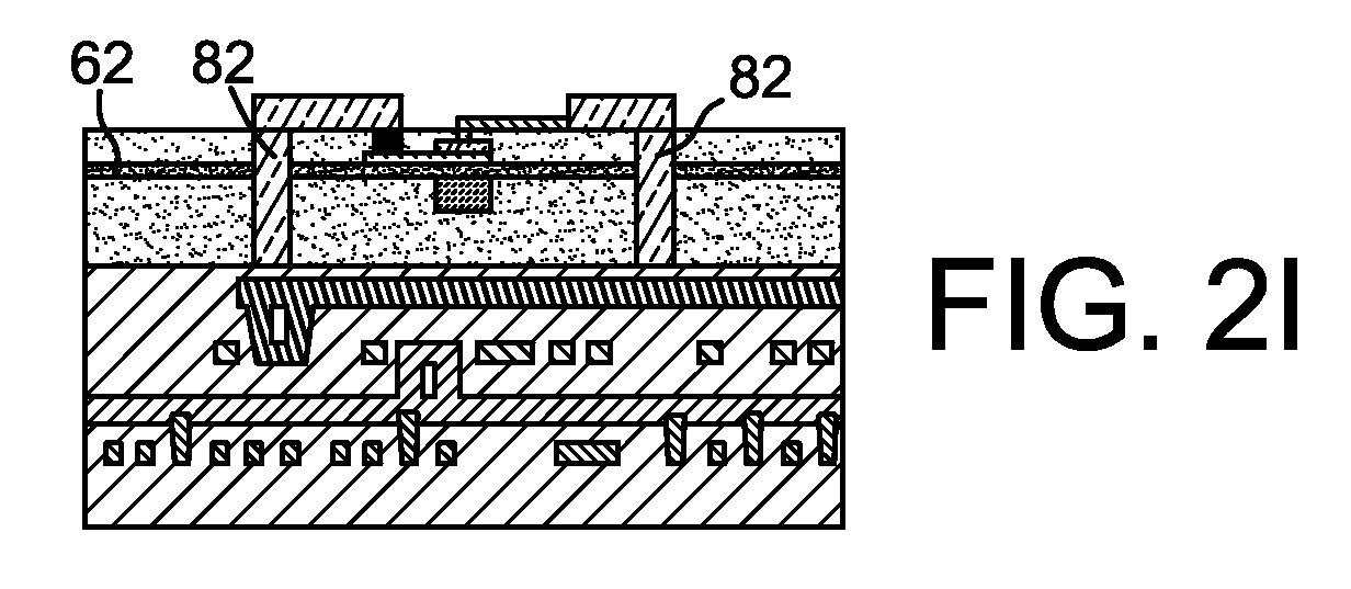
- the silicon substrate 60 is then eliminated up to the surface of the layer 62 ( Figure 2F). We obtains an optoelectronic component 69.
- components active optics 70 for example by adhesion molecular.
- Components 70 at least one source such as for example a laser transmitter and / or one or more photodetectors, for example in III-V materials.
- An exemplary embodiment of such components 70 will be described in more detail in connection with Figures 3A - 3H.
- the distance d, between the guide and the optically active means 70, is mainly defined by the thickness of this oxide layer 62: it can be weak, for example of the order of 70 nm to 420 nm.
- the oxide thickness can be controlled whatever the value of the distance d with an accuracy of +/- 10 nm at the substrate scale (8 inches), which allows to ensure optimum coupling throughout the entire substrate, thus ensuring good yields of particularly advantageous in the of an industrial process.
- a distance of weak for example in the range above, ensures a good coupling electromagnetic between the guide and each photodetector or transmitter concerned.
- the layer 62 can be thinned with techniques of chemical etching or plasma of the microelectronics (for example after the step of figure 2F) which still make it possible to remove a weak silica thickness, typically of the order of 100 nm, with great precision.
- the prior assembly of the layer comprising the optical guiding means with the electronic circuit 68 allows easy control of the distance d, before assembly with the means optically active.
- Tolerances for oxide deposition 67 as well as for polishing this oxide layer are relaxed (thickness after polishing preferably greater than 1 ⁇ m) and there is no need for control thick after polishing.
- Figures 3A-3H illustrate an example of realization of active optical components from an active plate comprising an InP substrate 170, a sacrificial layer 172 made of InGaAs, a heterostructure 174 (i.e., a stack of alternating layers of different compositions) thickness of the order of a few hundred nm, by example between 300 nm and 700 nm, for example 500 nm, a contact zone 176 (for example about 100 nm thick), and a silica layer 178 (by example of about 10 nm thick).
- an active plate comprising an InP substrate 170, a sacrificial layer 172 made of InGaAs, a heterostructure 174 (i.e., a stack of alternating layers of different compositions) thickness of the order of a few hundred nm, by example between 300 nm and 700 nm, for example 500 nm, a contact zone 176 (for example about 100 nm thick), and a silica layer 178 (
- This plate is assembled ( Figure 3B) with the assembly 69, illustrated in FIG. 2F, already produced, guiding means and electronic components.
- the assembly uses adhesive bonding molecular of the two plates.
- the heterostructure 174 for example a active component such as a light source (diode laser or microlaser) or a detector.
- a planarization step may have then take place (FIG. 3F) by depositing a layer 180 of polymer such as BCB.
- the distance between the guide and optically active means 179 remains easily controllable because, as already indicated above, prior assembly of the layer comprising the optical guiding means with the electric circuit.
- the example was given of a layer 64 in monocrystalline silicon, but it can be a layer of another material, of index superior to that of the oxide layer 62, for example a polymer or a nitride or a polycrystalline silicon layer.
Landscapes
- Physics & Mathematics (AREA)
- General Physics & Mathematics (AREA)
- Optics & Photonics (AREA)
- Engineering & Computer Science (AREA)
- Microelectronics & Electronic Packaging (AREA)
- Optical Integrated Circuits (AREA)
- Solid State Image Pick-Up Elements (AREA)
- Optical Couplings Of Light Guides (AREA)
- Light Receiving Elements (AREA)
- Led Device Packages (AREA)
Abstract
Description
- un émetteur 2 de lumière (diode électroluminescente ou diode laser) couplé à un guide 4 submicronique à fort indice,
- un arbre 6 de distribution,
- des photodétecteurs 8, 10 couplés en bout de chaque extrémité d'arbre.
- La figure 1 représente un dispositif connu,
- les figures 2A - 2I représentent des étapes d'un procédé selon l'invention,
- les figures 3A - 3H représentent des étapes de réalisation de sources de rayonnement avec une plaque sur substrat InP.
Claims (20)
- Procédé de réalisation d'un dispositif optoélectronique, comportant :a - une étape de réalisation de moyens (66) de guidage optique, dans une couche superficielle (64) d'un substrat composite, comportant un substrat support (60), une couche intermédiaire (62) en oxyde, dont le matériau a un indice optique inférieur à celui de la couche superficielle (64), et la couche superficielle.b - une étape d'assemblage de ces moyens avec des moyens (68) de circuit électronique,c - une étape d'élimination du substrat support (60)d - la formation de moyens (70) optiquement actifs par dessus cet assemblage, sur la couche intermédiaire, ladite couche intermédiaire ayant une épaisseur permettant d'assurer un bon couplage électromagnétique entre les moyens optiquement actifs et les moyens de guidage.
- Procédé selon la revendication 1, le substrat support étant en un matériau semi-conducteur.
- Procédé selon la revendication 2, la couche intermédiaire, d'indice optique inférieur à celui de la couche superficielle, étant en un oxyde du matériau semi-conducteur.
- Procédé selon la revendication 3, dans lequel la couche intermédiaire est en oxyde thermique.
- Procédé selon l'une des revendications 1 à 4, la couche intermédiaire, d'indice optique inférieur à celui de la couche superficielle ayant un indice inférieur à 1,6.
- Procédé selon l'une des revendications 1 à 5, le substrat composite étant de type SOI.
- Procédé selon l'une des revendications 1 à 6, la couche superficielle (64) étant en polymère ou en nitrure ou en silicium polycristallin.
- Procédé selon l'une des revendications 1 à 7, la couche intermédiaire (62) ayant une épaisseur comprise entre 50 nm et 1 µm, avantageusement entre 50 nm et 400 nm.
- Procédé selon l'une des revendications 1 à 8, comportant en outre une étape d'encapsulation dans une couche du matériau de la couche intermédiaire.
- Procédé selon l'une des revendications 1 à 9, l'étape b) étant réalisée par adhésion moléculaire ou par procédé SOG ou par l'intermédiaire d'un polymère ou par collage métallique ou eutectique.
- Procédé selon l'une des revendications 1 à 10, l'étape d) comprenant :d1- un assemblage d'une plaque active avec l'assemblage formé des moyens (66) de guidage optique et des moyens (38) de circuit électronique,d2- une formation des moyens (70) optiquement actifs dans la plaque active de cet assemblage.
- Procédé selon la revendication 11, la plaque active comportant un empilement de matériaux III - V.
- Procédé selon la revendication 11 ou 12, l'étape d1 étant obtenue par assemblage par adhésion moléculaire.
- Procédé selon l'une des revendications 11 à 13, les moyens (70) optiquement actifs étant réalisés par gravure dans la plaque active.
- Dispositif optoélectronique, comportant des moyens (66) de guidage optique, compris entre des moyens (68) de circuit électronique, et des moyens (70) optiquement actifs, une couche (62) intermédiaire d'oxyde, d'indice inférieur à l'indice du matériau constitutif des moyens de guidage optique, étant comprise entre ces moyens (66) de guidage optique et les moyens (70) optiquement actifs, l'épaisseur de la couche d'oxyde étant telle qu'elle permet d'assurer un bon couplage électromagnétique entre les moyens de guidage optique (66) et les moyens optiquement actifs (70).
- Dispositif selon la revendication 15, l'indice de la couche intermédiaire étant inférieur à 1,6.
- Dispositif selon la revendication 15 ou 16, dans lequel l'oxyde de la couche intermédiaire est un oxyde thermique.
- Dispositif selon l'une des revendications 15 à 17, la couche intermédiaire ayant une épaisseur comprise entre 50 nm et 1 µm, avantageusement entre 50 nm et 400 nm.
- Dispositif selon l'une des revendications 15 à 18, une distance d'au moins 1 µm séparant les moyens de guidage optique et les moyens (68) de circuit électronique.
- Dispositif selon l'une des revendications 15 à 19, les moyens (70) optiquement actifs étant en des matériaux de type III - V.
Applications Claiming Priority (2)
| Application Number | Priority Date | Filing Date | Title |
|---|---|---|---|
| FR0450535 | 2004-03-17 | ||
| FR0450535A FR2867898B1 (fr) | 2004-03-17 | 2004-03-17 | Fabrication d'une couche d'interconnection optique sur un circuit electronique |
Publications (2)
| Publication Number | Publication Date |
|---|---|
| EP1577690A1 true EP1577690A1 (fr) | 2005-09-21 |
| EP1577690B1 EP1577690B1 (fr) | 2008-02-27 |
Family
ID=34834282
Family Applications (1)
| Application Number | Title | Priority Date | Filing Date |
|---|---|---|---|
| EP05102029A Expired - Lifetime EP1577690B1 (fr) | 2004-03-17 | 2005-03-15 | Fabrication d'une couche d'interconnéction optique sur un circuit |
Country Status (5)
| Country | Link |
|---|---|
| US (1) | US7482184B2 (fr) |
| EP (1) | EP1577690B1 (fr) |
| AT (1) | ATE387639T1 (fr) |
| DE (1) | DE602005004945T2 (fr) |
| FR (1) | FR2867898B1 (fr) |
Cited By (1)
| Publication number | Priority date | Publication date | Assignee | Title |
|---|---|---|---|---|
| WO2014144590A1 (fr) * | 2013-03-15 | 2014-09-18 | Apic Corporation | Module photonique à puces multiples |
Families Citing this family (6)
| Publication number | Priority date | Publication date | Assignee | Title |
|---|---|---|---|---|
| US9442344B2 (en) * | 2014-06-02 | 2016-09-13 | Vadient Optics, Llc | Nanocomposite high order nonlinear optical-element |
| FR3054926B1 (fr) | 2016-08-08 | 2018-10-12 | Commissariat A L'energie Atomique Et Aux Energies Alternatives | Procede de fabrication d'un modulateur des pertes de propagation et de l'indice de propagation d'un signal optique |
| FR3061961B1 (fr) | 2017-01-19 | 2019-04-19 | Commissariat A L'energie Atomique Et Aux Energies Alternatives | Dispositif photonique comportant un laser optiquement connecte a un guide d'onde silicium et procede de fabrication d'un tel dispositif photonique |
| CN110828443A (zh) * | 2019-11-13 | 2020-02-21 | 中国科学院微电子研究所 | 无衬底光电混合集成结构及其制备方法 |
| FR3158372B1 (fr) | 2024-01-17 | 2025-12-05 | Scintil Photonics | Dispositif photonique comprenant une couche de composants disposée sur un substrat support et procédé de préparation d’un tel dispositif photonique |
| FR3170642A1 (fr) | 2024-12-23 | 2026-06-26 | Scintil Photonics | Procédé de préparation d’un dispositif photonique comportant une pluralité de guides d’onde hybrides apte à propager un mode optique |
Citations (2)
| Publication number | Priority date | Publication date | Assignee | Title |
|---|---|---|---|---|
| EP1041418A2 (fr) * | 1999-03-30 | 2000-10-04 | Toppan Printing Co., Ltd. | Couche d'interconnection optique, substrat d'interconnection optoélectrique, substrat monté et méthode de fabrication |
| WO2004010192A2 (fr) * | 2002-07-22 | 2004-01-29 | Applied Materials Inc. | Substrats a compatibilite optique |
Family Cites Families (4)
| Publication number | Priority date | Publication date | Assignee | Title |
|---|---|---|---|---|
| JP2001274528A (ja) * | 2000-01-21 | 2001-10-05 | Fujitsu Ltd | 薄膜デバイスの基板間転写方法 |
| US20030110808A1 (en) * | 2001-12-14 | 2003-06-19 | Applied Materials Inc., A Delaware Corporation | Method of manufacturing an optical core |
| US7072534B2 (en) * | 2002-07-22 | 2006-07-04 | Applied Materials, Inc. | Optical ready substrates |
| US6993225B2 (en) * | 2004-02-10 | 2006-01-31 | Sioptical, Inc. | Tapered structure for providing coupling between external optical device and planar optical waveguide and method of forming the same |
-
2004
- 2004-03-17 FR FR0450535A patent/FR2867898B1/fr not_active Expired - Fee Related
-
2005
- 2005-03-15 EP EP05102029A patent/EP1577690B1/fr not_active Expired - Lifetime
- 2005-03-15 DE DE602005004945T patent/DE602005004945T2/de not_active Expired - Lifetime
- 2005-03-15 AT AT05102029T patent/ATE387639T1/de not_active IP Right Cessation
- 2005-03-16 US US11/080,645 patent/US7482184B2/en not_active Expired - Lifetime
Patent Citations (2)
| Publication number | Priority date | Publication date | Assignee | Title |
|---|---|---|---|---|
| EP1041418A2 (fr) * | 1999-03-30 | 2000-10-04 | Toppan Printing Co., Ltd. | Couche d'interconnection optique, substrat d'interconnection optoélectrique, substrat monté et méthode de fabrication |
| WO2004010192A2 (fr) * | 2002-07-22 | 2004-01-29 | Applied Materials Inc. | Substrats a compatibilite optique |
Non-Patent Citations (1)
| Title |
|---|
| GEORGAKILAS A ET AL: "WAFER-SCALE INTEGRATION OF GAAS OPTOELECTRONIC DEVICES WITH STANDARD SI INTEGRATED CIRCUITS USING A LOW-TEMPERATURE BONDING PROCEDURE", APPLIED PHYSICS LETTERS, vol. 81, no. 27, 30 December 2002 (2002-12-30), pages 5099 - 5101, XP001144665, ISSN: 0003-6951 * |
Cited By (1)
| Publication number | Priority date | Publication date | Assignee | Title |
|---|---|---|---|---|
| WO2014144590A1 (fr) * | 2013-03-15 | 2014-09-18 | Apic Corporation | Module photonique à puces multiples |
Also Published As
| Publication number | Publication date |
|---|---|
| ATE387639T1 (de) | 2008-03-15 |
| EP1577690B1 (fr) | 2008-02-27 |
| FR2867898B1 (fr) | 2006-09-15 |
| DE602005004945T2 (de) | 2009-03-12 |
| FR2867898A1 (fr) | 2005-09-23 |
| DE602005004945D1 (de) | 2008-04-10 |
| US20060001038A1 (en) | 2006-01-05 |
| US7482184B2 (en) | 2009-01-27 |
Similar Documents
| Publication | Publication Date | Title |
|---|---|---|
| EP3352312B1 (fr) | Dispositif photonique comportant un laser optiquement connecté à un guide d'onde silicium et procédé de fabrication d'un tel dispositif photonique | |
| EP2092618B1 (fr) | Dispositif laser a source laser et guide d'onde couples | |
| US9864134B2 (en) | Semiconductor structure and method for manufacturing a semiconductor structure | |
| US11675126B1 (en) | Heterogeneous integration of an electro-optical platform | |
| CA3036322A1 (fr) | Dispositif photonique comportant un laser optiquement connecte a un guide d'onde silicium et procede de fabrication d'un tel dispositif photonique | |
| EP1444541B1 (fr) | Dispositif electronique monolithique multicouches et procede de realisation d'un tel dispositif | |
| FR3007589A1 (fr) | Circuit integre photonique et procede de fabrication | |
| EP3994509B1 (fr) | Assemblage d'un composant semi-conducteur actif et d'un composant optique passif à base de silicium | |
| FR3060772A1 (fr) | Circuit photonique integre optimise | |
| FR2912552A1 (fr) | Structure multicouche et son procede de fabrication. | |
| EP0645654A1 (fr) | Procédé de réalisation d'une structure intégrée monolithique incorporant des composants opto-électroniques et structure ainsi réalisée | |
| EP1741136A2 (fr) | Procede de fabrication de circuits electroniques et optoelectroniques | |
| EP4092746A1 (fr) | Procédé de fabrication d'un dispositif optoélectronique | |
| FR3053538A1 (fr) | Source laser a semi-conducteur | |
| EP1577690B1 (fr) | Fabrication d'une couche d'interconnéction optique sur un circuit | |
| EP1920281A1 (fr) | Dispositif de couplage hermetique | |
| US9989703B2 (en) | Semiconductor structure and method for manufacturing a semiconductor structure | |
| EP2442164B1 (fr) | Procédé de fabrication d'un duplexeur optique | |
| EP4148470A1 (fr) | Procede de fabrication d'un systeme optoelectronique en photonique sur silicium comportant un dispositif optique couple a un circuit photonique integre | |
| EP4320471B1 (fr) | Procédé de fabrication d'un dispositif photonique pourvu d'au moins deux puces photoniques et dispositif photonique | |
| FR2913815A1 (fr) | PROCEDE DE CO-INTEGRATION DE SEMI-CONDUCTEURS, EN PARTICULIER SOI ET GeOI OU GaAsOI | |
| FR3155319A1 (fr) | Procédé de fabrication d'un dispositif photonique | |
| WO2018122493A1 (fr) | Dispositif de collimation | |
| CA3043644A1 (fr) | Procede de realisation collective d'une pluralite de puces optoelectroniques |
Legal Events
| Date | Code | Title | Description |
|---|---|---|---|
| PUAI | Public reference made under article 153(3) epc to a published international application that has entered the european phase |
Free format text: ORIGINAL CODE: 0009012 |
|
| AK | Designated contracting states |
Kind code of ref document: A1 Designated state(s): AT BE BG CH CY CZ DE DK EE ES FI FR GB GR HU IE IS IT LI LT LU MC NL PL PT RO SE SI SK TR |
|
| AX | Request for extension of the european patent |
Extension state: AL BA HR LV MK YU |
|
| 17P | Request for examination filed |
Effective date: 20060309 |
|
| AKX | Designation fees paid |
Designated state(s): AT BE BG CH CY CZ DE DK EE ES FI FR GB GR HU IE IS IT LI LT LU MC NL PL PT RO SE SI SK TR |
|
| RAP1 | Party data changed (applicant data changed or rights of an application transferred) |
Owner name: COMMISSARIAT A L'ENERGIE ATOMIQUE |
|
| GRAP | Despatch of communication of intention to grant a patent |
Free format text: ORIGINAL CODE: EPIDOSNIGR1 |
|
| GRAS | Grant fee paid |
Free format text: ORIGINAL CODE: EPIDOSNIGR3 |
|
| GRAA | (expected) grant |
Free format text: ORIGINAL CODE: 0009210 |
|
| AK | Designated contracting states |
Kind code of ref document: B1 Designated state(s): AT BE BG CH CY CZ DE DK EE ES FI FR GB GR HU IE IS IT LI LT LU MC NL PL PT RO SE SI SK TR |
|
| REG | Reference to a national code |
Ref country code: GB Ref legal event code: FG4D Free format text: NOT ENGLISH |
|
| REG | Reference to a national code |
Ref country code: CH Ref legal event code: EP |
|
| REG | Reference to a national code |
Ref country code: IE Ref legal event code: FG4D Free format text: LANGUAGE OF EP DOCUMENT: FRENCH |
|
| REF | Corresponds to: |
Ref document number: 602005004945 Country of ref document: DE Date of ref document: 20080410 Kind code of ref document: P |
|
| PG25 | Lapsed in a contracting state [announced via postgrant information from national office to epo] |
Ref country code: ES Free format text: LAPSE BECAUSE OF FAILURE TO SUBMIT A TRANSLATION OF THE DESCRIPTION OR TO PAY THE FEE WITHIN THE PRESCRIBED TIME-LIMIT Effective date: 20080607 Ref country code: FI Free format text: LAPSE BECAUSE OF FAILURE TO SUBMIT A TRANSLATION OF THE DESCRIPTION OR TO PAY THE FEE WITHIN THE PRESCRIBED TIME-LIMIT Effective date: 20080227 Ref country code: IS Free format text: LAPSE BECAUSE OF FAILURE TO SUBMIT A TRANSLATION OF THE DESCRIPTION OR TO PAY THE FEE WITHIN THE PRESCRIBED TIME-LIMIT Effective date: 20080627 |
|
| NLV1 | Nl: lapsed or annulled due to failure to fulfill the requirements of art. 29p and 29m of the patents act | ||
| PG25 | Lapsed in a contracting state [announced via postgrant information from national office to epo] |
Ref country code: AT Free format text: LAPSE BECAUSE OF FAILURE TO SUBMIT A TRANSLATION OF THE DESCRIPTION OR TO PAY THE FEE WITHIN THE PRESCRIBED TIME-LIMIT Effective date: 20080227 |
|
| BERE | Be: lapsed |
Owner name: COMMISSARIAT A L'ENERGIE ATOMIQUE Effective date: 20080331 |
|
| PG25 | Lapsed in a contracting state [announced via postgrant information from national office to epo] |
Ref country code: PL Free format text: LAPSE BECAUSE OF FAILURE TO SUBMIT A TRANSLATION OF THE DESCRIPTION OR TO PAY THE FEE WITHIN THE PRESCRIBED TIME-LIMIT Effective date: 20080227 Ref country code: SI Free format text: LAPSE BECAUSE OF FAILURE TO SUBMIT A TRANSLATION OF THE DESCRIPTION OR TO PAY THE FEE WITHIN THE PRESCRIBED TIME-LIMIT Effective date: 20080227 |
|
| REG | Reference to a national code |
Ref country code: IE Ref legal event code: FD4D |
|
| PG25 | Lapsed in a contracting state [announced via postgrant information from national office to epo] |
Ref country code: NL Free format text: LAPSE BECAUSE OF FAILURE TO SUBMIT A TRANSLATION OF THE DESCRIPTION OR TO PAY THE FEE WITHIN THE PRESCRIBED TIME-LIMIT Effective date: 20080227 Ref country code: MC Free format text: LAPSE BECAUSE OF NON-PAYMENT OF DUE FEES Effective date: 20080331 Ref country code: CZ Free format text: LAPSE BECAUSE OF FAILURE TO SUBMIT A TRANSLATION OF THE DESCRIPTION OR TO PAY THE FEE WITHIN THE PRESCRIBED TIME-LIMIT Effective date: 20080227 Ref country code: SK Free format text: LAPSE BECAUSE OF FAILURE TO SUBMIT A TRANSLATION OF THE DESCRIPTION OR TO PAY THE FEE WITHIN THE PRESCRIBED TIME-LIMIT Effective date: 20080227 Ref country code: DK Free format text: LAPSE BECAUSE OF FAILURE TO SUBMIT A TRANSLATION OF THE DESCRIPTION OR TO PAY THE FEE WITHIN THE PRESCRIBED TIME-LIMIT Effective date: 20080227 Ref country code: SE Free format text: LAPSE BECAUSE OF FAILURE TO SUBMIT A TRANSLATION OF THE DESCRIPTION OR TO PAY THE FEE WITHIN THE PRESCRIBED TIME-LIMIT Effective date: 20080527 Ref country code: IE Free format text: LAPSE BECAUSE OF FAILURE TO SUBMIT A TRANSLATION OF THE DESCRIPTION OR TO PAY THE FEE WITHIN THE PRESCRIBED TIME-LIMIT Effective date: 20080227 Ref country code: PT Free format text: LAPSE BECAUSE OF FAILURE TO SUBMIT A TRANSLATION OF THE DESCRIPTION OR TO PAY THE FEE WITHIN THE PRESCRIBED TIME-LIMIT Effective date: 20080721 |
|
| PG25 | Lapsed in a contracting state [announced via postgrant information from national office to epo] |
Ref country code: RO Free format text: LAPSE BECAUSE OF FAILURE TO SUBMIT A TRANSLATION OF THE DESCRIPTION OR TO PAY THE FEE WITHIN THE PRESCRIBED TIME-LIMIT Effective date: 20080227 |
|
| PLBE | No opposition filed within time limit |
Free format text: ORIGINAL CODE: 0009261 |
|
| STAA | Information on the status of an ep patent application or granted ep patent |
Free format text: STATUS: NO OPPOSITION FILED WITHIN TIME LIMIT |
|
| PG25 | Lapsed in a contracting state [announced via postgrant information from national office to epo] |
Ref country code: EE Free format text: LAPSE BECAUSE OF FAILURE TO SUBMIT A TRANSLATION OF THE DESCRIPTION OR TO PAY THE FEE WITHIN THE PRESCRIBED TIME-LIMIT Effective date: 20080227 Ref country code: LT Free format text: LAPSE BECAUSE OF FAILURE TO SUBMIT A TRANSLATION OF THE DESCRIPTION OR TO PAY THE FEE WITHIN THE PRESCRIBED TIME-LIMIT Effective date: 20080227 |
|
| 26N | No opposition filed |
Effective date: 20081128 |
|
| PG25 | Lapsed in a contracting state [announced via postgrant information from national office to epo] |
Ref country code: BE Free format text: LAPSE BECAUSE OF NON-PAYMENT OF DUE FEES Effective date: 20080331 |
|
| PG25 | Lapsed in a contracting state [announced via postgrant information from national office to epo] |
Ref country code: BG Free format text: LAPSE BECAUSE OF FAILURE TO SUBMIT A TRANSLATION OF THE DESCRIPTION OR TO PAY THE FEE WITHIN THE PRESCRIBED TIME-LIMIT Effective date: 20080527 |
|
| PG25 | Lapsed in a contracting state [announced via postgrant information from national office to epo] |
Ref country code: CY Free format text: LAPSE BECAUSE OF FAILURE TO SUBMIT A TRANSLATION OF THE DESCRIPTION OR TO PAY THE FEE WITHIN THE PRESCRIBED TIME-LIMIT Effective date: 20080227 |
|
| REG | Reference to a national code |
Ref country code: CH Ref legal event code: PL |
|
| PG25 | Lapsed in a contracting state [announced via postgrant information from national office to epo] |
Ref country code: CH Free format text: LAPSE BECAUSE OF NON-PAYMENT OF DUE FEES Effective date: 20090331 Ref country code: LI Free format text: LAPSE BECAUSE OF NON-PAYMENT OF DUE FEES Effective date: 20090331 |
|
| PG25 | Lapsed in a contracting state [announced via postgrant information from national office to epo] |
Ref country code: LU Free format text: LAPSE BECAUSE OF NON-PAYMENT OF DUE FEES Effective date: 20080315 Ref country code: HU Free format text: LAPSE BECAUSE OF FAILURE TO SUBMIT A TRANSLATION OF THE DESCRIPTION OR TO PAY THE FEE WITHIN THE PRESCRIBED TIME-LIMIT Effective date: 20080828 |
|
| PG25 | Lapsed in a contracting state [announced via postgrant information from national office to epo] |
Ref country code: TR Free format text: LAPSE BECAUSE OF FAILURE TO SUBMIT A TRANSLATION OF THE DESCRIPTION OR TO PAY THE FEE WITHIN THE PRESCRIBED TIME-LIMIT Effective date: 20080227 |
|
| PG25 | Lapsed in a contracting state [announced via postgrant information from national office to epo] |
Ref country code: GR Free format text: LAPSE BECAUSE OF FAILURE TO SUBMIT A TRANSLATION OF THE DESCRIPTION OR TO PAY THE FEE WITHIN THE PRESCRIBED TIME-LIMIT Effective date: 20080528 |
|
| REG | Reference to a national code |
Ref country code: FR Ref legal event code: PLFP Year of fee payment: 12 |
|
| REG | Reference to a national code |
Ref country code: FR Ref legal event code: PLFP Year of fee payment: 13 |
|
| REG | Reference to a national code |
Ref country code: FR Ref legal event code: PLFP Year of fee payment: 14 |
|
| PGFP | Annual fee paid to national office [announced via postgrant information from national office to epo] |
Ref country code: DE Payment date: 20240321 Year of fee payment: 20 Ref country code: GB Payment date: 20240318 Year of fee payment: 20 |
|
| PGFP | Annual fee paid to national office [announced via postgrant information from national office to epo] |
Ref country code: IT Payment date: 20240329 Year of fee payment: 20 Ref country code: FR Payment date: 20240320 Year of fee payment: 20 |
|
| REG | Reference to a national code |
Ref country code: DE Ref legal event code: R071 Ref document number: 602005004945 Country of ref document: DE |
|
| REG | Reference to a national code |
Ref country code: GB Ref legal event code: PE20 Expiry date: 20250314 |
|
| PG25 | Lapsed in a contracting state [announced via postgrant information from national office to epo] |
Ref country code: GB Free format text: LAPSE BECAUSE OF EXPIRATION OF PROTECTION Effective date: 20250314 |