EP1576761B1 - Method and device for extracting a clock pulse frequency underlying a data flow - Google Patents
Method and device for extracting a clock pulse frequency underlying a data flow Download PDFInfo
- Publication number
- EP1576761B1 EP1576761B1 EP03799504A EP03799504A EP1576761B1 EP 1576761 B1 EP1576761 B1 EP 1576761B1 EP 03799504 A EP03799504 A EP 03799504A EP 03799504 A EP03799504 A EP 03799504A EP 1576761 B1 EP1576761 B1 EP 1576761B1
- Authority
- EP
- European Patent Office
- Prior art keywords
- oscillator
- frequency
- data pattern
- digital
- tuning
- Prior art date
- Legal status (The legal status is an assumption and is not a legal conclusion. Google has not performed a legal analysis and makes no representation as to the accuracy of the status listed.)
- Expired - Lifetime
Links
- 238000000034 method Methods 0.000 title claims description 14
- 238000011084 recovery Methods 0.000 claims description 14
- 230000003247 decreasing effect Effects 0.000 claims description 8
- 238000004590 computer program Methods 0.000 claims description 7
- 238000001514 detection method Methods 0.000 claims description 5
- 230000008859 change Effects 0.000 claims description 4
- 230000007423 decrease Effects 0.000 claims description 3
- 230000002123 temporal effect Effects 0.000 claims 2
- AZFKQCNGMSSWDS-UHFFFAOYSA-N MCPA-thioethyl Chemical compound CCSC(=O)COC1=CC=C(Cl)C=C1C AZFKQCNGMSSWDS-UHFFFAOYSA-N 0.000 claims 1
- 238000010586 diagram Methods 0.000 description 9
- 239000013078 crystal Substances 0.000 description 8
- 238000012937 correction Methods 0.000 description 7
- 239000010453 quartz Substances 0.000 description 7
- VYPSYNLAJGMNEJ-UHFFFAOYSA-N silicon dioxide Inorganic materials O=[Si]=O VYPSYNLAJGMNEJ-UHFFFAOYSA-N 0.000 description 7
- 238000012546 transfer Methods 0.000 description 6
- 230000007704 transition Effects 0.000 description 6
- 238000005259 measurement Methods 0.000 description 5
- 230000005540 biological transmission Effects 0.000 description 4
- 230000010355 oscillation Effects 0.000 description 4
- 241000238876 Acari Species 0.000 description 3
- 238000004891 communication Methods 0.000 description 3
- 238000000605 extraction Methods 0.000 description 3
- 238000013459 approach Methods 0.000 description 2
- 230000006870 function Effects 0.000 description 2
- 230000008929 regeneration Effects 0.000 description 2
- 238000011069 regeneration method Methods 0.000 description 2
- 230000004044 response Effects 0.000 description 2
- 101100115778 Caenorhabditis elegans dac-1 gene Proteins 0.000 description 1
- 230000015556 catabolic process Effects 0.000 description 1
- 230000006378 damage Effects 0.000 description 1
- 238000013075 data extraction Methods 0.000 description 1
- 238000006731 degradation reaction Methods 0.000 description 1
- 230000001934 delay Effects 0.000 description 1
- 230000003111 delayed effect Effects 0.000 description 1
- 238000013461 design Methods 0.000 description 1
- 230000005611 electricity Effects 0.000 description 1
- 238000005516 engineering process Methods 0.000 description 1
- 230000002452 interceptive effect Effects 0.000 description 1
- 230000008520 organization Effects 0.000 description 1
- 230000000737 periodic effect Effects 0.000 description 1
- 230000010363 phase shift Effects 0.000 description 1
- 229920000729 poly(L-lysine) polymer Polymers 0.000 description 1
- 230000009467 reduction Effects 0.000 description 1
- 230000001172 regenerating effect Effects 0.000 description 1
- 230000001360 synchronised effect Effects 0.000 description 1
- 230000001960 triggered effect Effects 0.000 description 1
Images


Classifications
-
- H—ELECTRICITY
- H03—ELECTRONIC CIRCUITRY
- H03L—AUTOMATIC CONTROL, STARTING, SYNCHRONISATION OR STABILISATION OF GENERATORS OF ELECTRONIC OSCILLATIONS OR PULSES
- H03L7/00—Automatic control of frequency or phase; Synchronisation
- H03L7/06—Automatic control of frequency or phase; Synchronisation using a reference signal applied to a frequency- or phase-locked loop
- H03L7/08—Details of the phase-locked loop
- H03L7/099—Details of the phase-locked loop concerning mainly the controlled oscillator of the loop
- H03L7/0995—Details of the phase-locked loop concerning mainly the controlled oscillator of the loop the oscillator comprising a ring oscillator
-
- H—ELECTRICITY
- H04—ELECTRIC COMMUNICATION TECHNIQUE
- H04L—TRANSMISSION OF DIGITAL INFORMATION, e.g. TELEGRAPHIC COMMUNICATION
- H04L7/00—Arrangements for synchronising receiver with transmitter
- H04L7/04—Speed or phase control by synchronisation signals
- H04L7/041—Speed or phase control by synchronisation signals using special codes as synchronising signal
- H04L7/046—Speed or phase control by synchronisation signals using special codes as synchronising signal using a dotting sequence
-
- H—ELECTRICITY
- H03—ELECTRONIC CIRCUITRY
- H03L—AUTOMATIC CONTROL, STARTING, SYNCHRONISATION OR STABILISATION OF GENERATORS OF ELECTRONIC OSCILLATIONS OR PULSES
- H03L2207/00—Indexing scheme relating to automatic control of frequency or phase and to synchronisation
- H03L2207/50—All digital phase-locked loop
Definitions
- USB Universal Serial Bus
- the USB standard standardizes a data transfer format for fast data transfer between USB devices and a host.
- the USB standard defines a so-called Tier-Star topology, where USB devices can either be hubs or functions or functional devices.
- the USB data format is specified in the USB specification.
- the most recent USB definition is currently USB Revision 2.0.
- the USB bus is a half-duplex bus. All transactions are initiated by the host.
- the USB specification revision 2.0 defines three data transfer rates. The lowest data transfer rate is used in low-speed mode, and is 1.5 megabits per second. In full-speed mode, a data transfer rate of 12 megabits per second is used. In high-speed mode, a data transfer rate of 480 megabits per second is used.
- the use of the low-speed mode is for interactive devices such. As a keyboard or a mouse. Only a limited number of low-speed devices should be connected to the bus to avoid degradation of bus utilization. For full-speed and high-speed devices, special bandwidth and latency are guaranteed.
- Devices are connected to the USB bus via a 4-wire cable that carries differential data, a power signal, and ground.
- a 4-wire cable that carries differential data, a power signal, and ground.
- Dp positive differential signal
- Dn negative difference signal
- the clock information is encoded in the data.
- an NRZI coding and a bit stuffing technique is used to guarantee an adequate number of transitions.
- NRZI means No Return to Zero Invert. This means that an inverse coding is used.
- a logic "1" signal is represented by a non-existent change in the electrical signal, while a logic "0" signal is represented by a change in the state of the electrical signal.
- An edge thus represents a zero, while a non-existent change, ie a constant signal represents a zero.
- a bit stuffing is used for DC reduction, so that after six consecutive ones, a positive / negative edge is used.
- the data stream is defined as a sequence of frames or frames 72, 73 which are separated by so-called control 74, with the ticks occurring at 1 ms intervals.
- frame 72 or 73 are a plurality of data packets.
- a frame consists of several data packets, and that a data stream is composed of a plurality of consecutive frames.
- Each data packet is introduced in the data stream from a packet identification number which has a width of 8 bits and is shown in Fig. 7c.
- a frame therefore includes as many packet identification numbers (PIDs) as there are packets in the frame.
- the packet identification number specification shown in Figure 7c which is four bits wide and is represented in a PID field by the four PID 0 , PID 1 , PID 2 , PID 3 PID bits and the corresponding inverted PID bits , is set in the USB standard.
- the bits shown in Fig. 7c are arranged from LSb to MSb. LSb stands for Least Significant Bit, while MSb stands for Most Significant Bit.
- the host transmits a start of frame (SOF) packet once per millisecond to define the ticks 74 shown in Figure 7b.
- SOF start of frame
- the SOF packet is shown in FIG. 7d and includes a SYNC field (not shown in FIG. 7d), a SOF PID field 75, an 11-bit frame number (76) (frame number), and a CRC.
- the frame number 76 is incremented by 1 with each additional SOF packet.
- the PID field 75 of Fig. 7d preceding synchronization pattern is shown as an electrical signal. It consists of a sequence of bits specified in the USB standard or a data pattern which, due to the NRZI coding, looks like an electrical signal, as shown in FIG. 7a.
- the sequence of data bits is 00000001, resulting in the "electrical" sequence 10101011 shown in FIG. 7a.
- Idle In front of the synchronization data pattern is an area labeled Idle, which has a single-ended-zero (SE0) coding with respect to the difference signals Dp and Dm, as set forth below.
- This SE0 coding of the Dp and Dm signals points to the end of a previous frame and further indicates that now follows a new frame which is introduced with a sync field immediately, as shown in Figure 7a , the packet identification number, and specifically, as shown in Fig. 7c, a least significant bit of the PID followed by the next higher bit of the PID, etc. follows.
- Fig. 7a illustrates that the bits in the synchronization pattern are fixed and the associated electrical signal may have the sequence of 10101011 while the PID bits may have both a 0 and a 1 depending on the packet identification to be coded.
- Each low-speed or full-speed data packet transmitted via the USB bus thus starts with a synchronization pattern ( Figure 7a) followed by the packet identification number (PID) shown in Figure 7c. which defines the package type.
- the sync field includes a series of 0-1 transitions on the bus to allow a receiver to synchronize to the bit clock.
- a frame interval of one millisecond is defined.
- the host transmits an SOF packet (frame start packet) once every millisecond ( Figure 7b).
- the SOF packet consists of a synchronization field followed by the SOF PID, an 11-bit frame number, and a CRC 5 fingerprint ( Figure 7d).
- the frame number is incremented with each sent SOF packet.
- a boot sequence occurs. At the end of this sequence, the device is driven to a reset state. After the reset event, the device has a duration of 10 milliseconds to perform a reset recovery. During this time, the device receives SOF packets.
- a conventional USB device is shown schematically in FIG. It includes an analog USB front-end that may be integrated with a differential transmitter (TX) and a differential receiver (RX) in a functional unit 90.
- TX differential transmitter
- RX differential receiver
- the signals Dp and Dm are in analog form, while on another side of the element 90, the corresponding received and analog / digital converted signals are applied, which are fed to a USB core 91 and received by the same become.
- These signals are represented in FIG. 9 by the two pairs of parallel signal arrows.
- the USB device further includes a quartz oscillator 92, which is in communication with a Quarzoszillatorbesciens 93, wherein the Quarzoszillatorbesciens 93 on the one hand the USB core 91 and on the other hand a clock distribution 94 drives, which is ally with a CPU 95, which in turn is connected to a memory 96 in operative connection.
- a USB device also includes a parallel input-output interface (parallel I / O) 97.
- such conventional USB devices typically use a quartz oscillator 92 as the clock source for the system devices and the USB data recovery circuit.
- quartz oscillator 92 For rugged portable devices, such as portable devices. Smart cards, it would be desirable to extract their own local clock directly from the USB data stream.
- quartz oscillators is impractical since quartz crystals can not normally be integrated into a chip and are also very susceptible to destruction due to mechanical stress. Smart cards are usually worn in harsh environments, such. B. in a wallet, which is housed in a trouser pocket. The mechanical stress exerted thereby would be fatal for a quartz crystal.
- US 2001/0011914 A1 discloses an apparatus for recovering a clock signal from at least two synchronization bits.
- a reference clock signal a signal from an internal oscillator is used to measure the number of reference clock pulses between the first two synchronization pulses sent from an external USB bus at the beginning of each transaction.
- N a rough measurement for the USB clock signal to be regenerated is obtained.
- the delay of each of these two sync pulses with respect to the previous pulse of the reference clock signal is being measured. This delay is calculated with respect to an internally defined time unit. Based on the measurement of these two delays and the measurement of a number of reference clock periods.
- US 2001/0020857 A1 discloses an apparatus for regenerating a clock signal from an external serial bus, the apparatus comprising a ring oscillator and a counter.
- the ring oscillator provides n phases of a clock signal. Of these n-phases, one phase is used as a reference and applied to the counter. It is therefore possible to count the number of total reference clock signal periods between a first pulse and a second pulse obtained from the bus. Upon reading the state of the phases in the oscillator receiving the second pulse, a current phase corresponding to the phase shift between the reference clock signal and the second pulse of the bus is determined.
- a regeneration device which also includes a ring oscillator and a counter, it is possible to regenerate the clock signal on the bus with high accuracy.
- U.S. Patent No. 6,343,364 B1 discloses a method and apparatus for local clock generation using the USB signals Dp and Dm, which operates without quartz oscillator or resonator. For this purpose, a number of cycles of a freewheeling high-frequency clock signal is counted, which occurs in a known number of bit periods of the received signal. Thereafter, the counted number of cycles of the freewheeling high frequency signal is divided by the known number of bit periods to determine a resulting number of clock cycles included in a single bit duration of the received USB signal. Based on this, a local clock signal is generated.
- WO 00/16255 discloses a method for data transmission and a smart card suitable for this purpose.
- the signals Dp and Dm are connected to an interface of the card.
- the card further includes a CPU, memory units, USB output contacts, and an array of at least six pads that are planar with the surface of the card body.
- U.S. Patent No. 5,487,084 discloses a concept for generating a clock frequency in a smart card interface used for data transmission from a smart card to, for example, a mobile telephone, to obtain a predetermined data rate.
- a phase locked loop and a number of programmable counters are used to obtain a clock signal having a frequency that is a multiple of the data rate.
- the counters and the phase-locked loop can be chosen so that the frequency is 16 times such a data rate in order to use a universal asynchronous receiver / transmitter (UART).
- U.S. Patent No. 5,818,948 discloses an architecture for a USB based PC speaker control device. To recover a clock from the received data stream, a phase locked loop is used.
- U.S. Patent No. 6,061,802 discloses software-based clock synchronization with an isochronous master clock structure in which the frame rate clocks of a plurality of data buses are synchronized to a master clock signal.
- the master clock signal is derived from the existing clock signals within the computer system or from data received from an external source.
- U.S. Patent No. 6,092,210 discloses an apparatus and method for synchronizing the clocks of connected USB buses by synchronizing clocks in a local device to the data streams of both USB buses. For this purpose, a separate local clock synchronization device is used for each USB device connected to the USB device under consideration is. Each separate local clock synchronization can use the same reference clock.
- DE 10041772 C2 discloses a clock generator, in particular for USB devices, in which a pulse filter is triggered on the basis of a periodically recurring in the data stream synchronization signal to a frequency of a pulse train, which is output from an internal clock generator by suppressing pulses in the effective frequency to reduce. Further, using the synchronization signal and a value stored in a pulse number memory or using an output signal of a data signal decoder, a frequency generated by the internal clock generator is retuned.
- US Pat. No. 6,407,641 B1 discloses an auto-locking oscillator for data communication. To tune the oscillation frequency of a clock signal, the frequency of an incoming data stream is analyzed to produce one or more control signals, and the oscillation frequency is adjusted to the one or more signals accordingly. Between a data stream analyzer and the oscillator to be set, a coarse-tuning device and a fine-tuning device are connected.
- U.S. Patent No. 6,125,158 discloses a phase rain loop and a multistage phase comparator.
- the comparator measures a phase difference between a reference signal and an output signal using a periodic clock.
- the comparator is a two-stage comparator with a fine comparator and a coarse comparator.
- the coarse comparator measures the number of clock periods between the transitions of the reference signal and the output signal.
- the fine comparator includes a delay line generator that generates a plurality of delayed clocks. These are then used to sample the reference signal to determine a fine phase difference between transitions of the reference signal and the output signal.
- EP 0414445 A2 discloses a digital frequency synthesizer having a phase accumulator comprising a coarse-component accumulator and a fine-component accumulator together with a dithering circuit.
- the fine component accumulator controls the coarse-component accumulator, which in turn feeds a non-linear DAW.
- the object of the present invention is to provide an on the one hand economical and on the other hand accurate concept for extracting a clock frequency underlying a data stream.
- the present invention is based on the finding that even for faster USB modes, the synchronization field alone or the duration of the synchronization field is at least sufficient to achieve a coarse adjustment of an oscillating within free limits oscillator.
- the achievable accuracy for the adjustment of the free-running oscillator is far too low to perform a meaningful data extraction.
- it is already sufficiently accurate to start with coarse data retrieval to decode the packet identification field following the sync field.
- the number of clock periods of the free-running oscillator between two temporally successive packet identification fields is counted and compared with a predetermined reference value.
- the present invention is thus based on the fact that, although a time jitter is allowed for consecutive USB clocks of 12 ns and 20 ns respectively, the accuracy for a frame interval, ie for the distance between two consecutive frame start packet identifications, is set much narrower in percentage terms is.
- the USB standard defines a frame interval of 1 ms ⁇ 500 ns. This corresponds to a relative accuracy of 0.05%. According to the invention, therefore, the high relative accuracy frame period is used to achieve fine tuning of the clock recovery oscillator.
- fine tuning on the basis of the frame period ie the first data pattern in a preferred embodiment only after the coarse tuning has taken place on the basis of the synchronization field, as in the preferred embodiment frame identification number decoding works well after coarse tuning has taken place.
- the concept according to the invention is advantageous in that a two-step approach is used in which the fine tuning builds on the coarse tuning and thus enables clock recovery without external quartz crystals or complex non-integrable resonators for devices that operate at high data rates, such. USB high-speed mode or USB full-speed mode.
- the inventive concept is also advantageous in that the use of simple and thus robust algorithms is possible, so that a simple and at the same time robust implementation z. B. on portable devices such as smart cards, etc., which are also limited in terms of computing power and in terms of memory requirements per se.
- coarse tuning is performed on the basis of a second data pattern existing in the data stream, which is preferably easily detectable, and fine-tuning is performed on the basis of first data patterns repeating in the data stream, the recurring first data patterns being present with high accuracy, however, are not as easily detectable as a second data pattern.
- This achieves clock recovery with the high accuracy on which the recurring first data pattern in the data stream is based, but for the detection of which a coarse tuning of the oscillator on the basis of the second data pattern, which is easily detectable but inaccurately present, is used.
- the two-stage concept according to the invention makes it possible to achieve, on the one hand, fast and, on the other hand, accurate frequency adjustment.
- the coarse tuning z. B. performed with the first synchronization pattern, so that in the startup time of 10 ms enough successive events in the data stream (eg., SOF PIDs) remain that a secure and accurate tuning of the now roughly co-tuned oscillator is achieved.
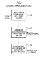
- 1 shows a device for extracting a clock frequency underlying a data stream, wherein the data stream at regular, with a relative first accuracy specified first time intervals such. For example, 1 ms for an application for a USB data stream, a first data pattern such.
- B. a frame start packet identification number (SOF PID) and wherein the data stream further comprises a second data pattern (synchronization field) having a plurality of clock periods according to the clock frequency or a multiple of the clock frequency, wherein the clock periods are specified with a second relative accuracy that is less than the first relative accuracy.
- SOF PID frame start packet identification number
- the inventive device is designed to control a controllable oscillator 10, d. H. to supply an oscillator controller 11 with coarse tuning signals on a line 12a or fine tuning signals on a line 12b, such that the oscillator controller 11 provides the controllable oscillator 10 with a corresponding voltage signal in the case of a VCO or a corresponding current signal in the case depending on the design of the controllable oscillator an ICO can supply.
- the device according to the invention comprises a coarse tuning device 13 and a fine tuning device 14.
- the coarse tuning device is designed to detect a start and an end of the second data pattern (synchronization field using the example of the USB specification).
- the coarse tuning device is further configured to count a number of clock periods of the controllable oscillator 10 in a time period from the beginning to the end of the second data pattern.
- the coarse tuning means is arranged to drive the oscillator control means 11 to reduce the oscillator clock frequency of the controllable oscillator 10, or in the case where the counted number less than the reference value is to drive the controllable oscillator to increase its oscillator clock frequency.
- the fine tuning device 14 is formed. In contrast to the coarse-tuning device, however, it does not detect the start and the end of the second data pattern but rather the occurrence of a first data pattern in the data stream and a subsequent occurrence of the first data pattern in the data stream.
- the fine-tuning device is further configured to count the number of clock periods of the oscillator 10 from an occurrence of the first data pattern to a next occurrence of the first data pattern, and then to control the oscillator controller 11 according to the location of the counted value with respect to a set reference value Oscillation frequency of the controllable oscillator 10 is increased or decreased. Only in happy isolated cases is the oscillator already set correctly due to the coarse tuning.
- an oscillator clock frequency is obtained with the relative second accuracy, that is, the accuracy underlying the first data pattern, which, depending on the specific embodiment, is immediately equal to the clock that underlies the data stream, or equal to a multiple of the clock, underlying the data stream, or equal to a fraction of the clock underlying the data stream.
- integer multiples such. For example, two times, three times, .... n times, where n is an integer.
- fractions are also integer fraction preferred, such. B. 1/2, 1/3, 1/4, ...., 1 / n, where n is also an integer.
- FIG. 1 shows a device 130 for detecting the beginning and the end of the second data pattern in the data stream, that is to say using the example of the USB data stream z.
- B the beginning of the synchronization pattern in the form of the first electrical "1” and the end of the synchronization pattern in the form of the last electrical "1" of the synchronization pattern of Fig. 7a.
- only a portion of the synchronization pattern of FIG. 7a may be used as a second data pattern, such that the second data pattern used for coarse tuning purposes begins with the first electrical "1" and with the first seventh logical "0" ends such that only the alternate part of the synchronization pattern of Fig. 7a is used.
- only part of the alternating bit pattern could be used depending on the ratio of the frequency of the controllable oscillator to the bit clock used in FIG. 7a.
- means 131 for counting the oscillator periods between the start detected by the device 130 and the end detected by the device 130 are operated. Specifically, by a counter enable signal output by the device 130 when it detects the beginning of the second data pattern, a counter is started which counts the clock periods of the oscillator signal supplied to the device 131 until the end 130 is detected by the device 130 or according to the counter-stop signal from the device 130 to the device 131 is transmitted.
- the count may then be supplied by means 131 to means 132 configured to compare the count to a reference value and to provide a corresponding correction signal which is communicated to the oscillator controller (means 11 of FIG. 1).
- the reference value used by the device 132 depends on a nominal frequency of the oscillator 10 and a time duration or number of considered bits of the synchronization pattern shown in Fig. 7a or a part thereof. If the bit clock of the synchronization pattern in Fig. 7a z.
- the predetermined reference value will be 64.
- the controllable oscillator 10 during the duration of the synchronization pattern of Fig. 7a would have to provide 64 clocks. If he delivers less than 64 bars, he is too slow. If he delivers more than 64 measures, it is too fast.
- Fig. 3 shows a more detailed block diagram of the fine-tuning device 14 of Fig. 1.
- the fine-tuning device 14 of Fig. 1 comprises means 140 for detecting a first data pattern (a SOF PID using the example of the USB format) and a temporally following first data pattern.
- a counter is activated in a means 141 for counting the oscillator periods in a first data pattern, which is then stopped when a temporally following first data pattern has been detected.
- the counter in the device 141 is operative to count the clock periods of the controllable oscillator 10 of FIG.
- the count value is then applied to a means 142 which is adapted to compare this count value with a reference value and to generate the correction signal supplied to the oscillator controller 11 of FIG.
- the time interval between two consecutive first data patterns is 1 ms, as shown in FIG. 7b.
- the nominal frequency of the controllable oscillator 10 of FIG. 1 is 96 MHz again, then the predetermined reference value would be 96,000, d. H. it would take 96,000 oscillator cycles in the 1 millisecond time to set the oscillator correctly. If the count is greater than 96,000, the oscillator frequency must be reduced. If the count is less than 96,000, the oscillator frequency must be increased.
- the fine-tuning device shown in Fig. 3 may be further used as a frequency tracing device after both coarse tuning and fine tuning are completed, and the accuracy or frequency-following capability of the Oscillator should be further increased, as will be explained below.
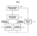
- the devices 132 of FIG. 2 or 142 of FIG. 3 are preferably designed to work iteratively, as will be explained below with reference to FIG. 4.
- the iterative approach is to first measure (40) the number of clock cycles through devices 130 and 140, respectively, to then compare the measured number to a reference value (41). If the comparison result is that the number of clock cycles is greater than the reference value, the frequency is reduced (42). On the other hand, if it is determined that the measured number of clock cycles is less than the reference value, the frequency of the oscillator must be increased (43 ). Then an iteration variable is incremented or entered into a next step 44, in which it is now checked again whether the frequency increased or decreased in the last value is again too high or too low.
- the 1 ms frame interval is used to set the frequency of the free running oscillator.
- the frequency accuracy of the oscillator is within the specified range of 0.25%.
- a tuning of the oscillator is performed in two sections, namely first in a coarse tuning section and then in one
- the measurement based on SYNC bits can not further improve the accuracy of the oscillator frequency. Now the fine tuning begins.
- the frequency of the oscillator after the tuning thereof is determined by the reference value FR.
- the reference value FR must be equal to 96,000 when contemplating successive SOF packets.
- the reference value is correspondingly higher.
- the reference value is correspondingly lower.
- a frequency tracking algorithm that further adjusts the oscillator frequency takes place.
- the number of oscillator periods between SOF packets present in the data stream is measured.
- the oscillator clock obtained after coarse tuning and fine tuning can be used as a reference clock for a USB core.
- FIG. 8 in which the extraction device according to the invention, which is designated by 80, is shown.
- the extraction device according to the invention therefore has, together with a controllable oscillator, the functionality of the blocks 92 and 93 of the known USB function circuit, which has been explained with reference to FIG.
- phase locking between the oscillator clock and the bit clock of the USB data stream is not required since the oscillator clock frequency is usually a multiple of the bit clock frequency and oversampling and digital PLLs can be used for data recovery.
- the inventive device is advantageous in that for data streams, which is based on a fast clock, such. For example, for full-speed USB data streams and high-speed USB data streams, no crystal oscillator is needed. Of course, even for slower clocked data streams no external oscillators are needed.
- the device according to the invention is furthermore advantageous in that the regenerated frequency is obtained with high accuracy, which is determined by the accuracy with which the first data pattern is present in the data stream.
- the example of the USB application achieves an accuracy of 0.05%.
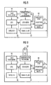
- Fig. 5 shows a clock regeneration circuit, which basically consists of two main units.
- One is the digitally controllable oscillator 50, which has an oscillator controller 11 on the one hand and the controllable oscillator 10 on the other hand, which is a current-controlled oscillator in FIG.
- FIG. 5 further shows a digital logic 52 including the coarse tuner 13 and the fine tuner 14, as illustrated below.
- the current controlled oscillator 10 is current-controlled in the preferred embodiment shown in FIG Ring oscillator with an odd number of in-line inverters 51a, 51b, 51c, which are supplied by a current summing node 52 with an operating current over which an oscillation frequency of the current-controlled oscillator 10 is adjustable.
- the oscillator control device 11 comprises, in addition to the current sum node 52, a supply current source or reference current source 53, which supplies a central reference (there is typically additionally a separate bias), a first digital / analog converter 54, a second digital / analog converter 55, and a
- the digital-to-analogue converters 54, 55 and 56 of FIG. 5 are designed to provide, on the output side, a current that is a fraction of the supply current supplied on the input side, wherein the selection of the fractional part over that of the Digital-to-analog converter via a digital input supplied binary number takes place.
- binary-weighted circuits 54, 55 and 56 are preferred.
- the DAW 1 (54) provides the value of the supply current 53 at its output to the current summation node 52 when all bits of the same supplied binary number are set. If, on the other hand, only the MSB of the DAW 1 (54) is set, while all the low-order bits are equal to 0, the DAW 1 supplies on the output side half of the current supplied by the source 53 to the current summation node. According to the invention, 9-bit DAWs are preferred, although in the embodiment also higher and lower width DAWs can be used.
- the DAW 1 54 is supplied directly by the power supply 53. It can therefore deliver the maximum amount of electricity on the output side.
- the DAW 1 is adjusted in a preferred embodiment of the present invention by the coarse tuning and the fine tuning. More specifically, the high order bits of the DAW 1 are adjusted by the coarse tuning, while the low order bits of the DAW 1 are adjusted by the fine tuning become.
- the DAW 2 55 is used for frequency tracking. Its supply current and thus the maximum of it to the current summation node 52-deliverable oscillator control current is controlled by the DAW 3 56.
- the output current of the DAW 3 56 is equal to the supply current 53, which leads directly to the fact that the DAW 2, if it is also supplied with all ones, can supply the same power to the summing node 52. According to the invention, however, it is preferred to apply a binary number to the DAW 3 which is smaller than the maximum loadable binary number in order to reduce the maximum current supplied by the DAW 2 55 to the current summation node 52.
- the DAW 2 55 can also be charged with 9 bits, for example, in order to be able to perform a frequency tracking to which the DAW 2 55 is used with a finer accuracy, as achieved by the LSB of the DAW 1 is determined.
- the granularity of the current output by the DAW.2 is inversely proportional to the operating current supplied to the DAW 2. The smaller the operating current supplied to the DAW 2 (set by the DAW 3), the finer the granularity in the frequency tracking mode following the fine tuning mode.
- the digitally controllable oscillator 11 thus comprises a supply source 53, the current controlled ring oscillator 10 and the three DAWs 54, 55 and 56.
- the DAWs controlled by the digital logic 52 provide the control current for frequency adjustment of the current controlled oscillator ICO 10.
- the total current for the ICO is the sum of the currents supplied by the two DAWs 54 and 55.
- the regions of the digital-to-analogue converters 1 and 2 are preferably overlapping. It is preferred that the maximum output current of the DAW 1 is a programmable multiple (programmable by the DAW 3) the maximum output of the DAW 2 is. Preferably, a factor of 4 is used.
- the DAW 3 56 is biased so that the supply current in the DAC 2 is smaller by the programmable multiple than the supply current in the DAC 1. It is further preferred that during coarse tuning and fine tuning, the MSB of the DAW 2 is set and / or all other bits of the DAW 2 are not set. The DAW 2 thus supplies half of the total maximum possible output current to the current summation node 52. If all the bits of the DAW are then set by the coarse tuning mode and the fine tuning mode, by additionally setting bits of the DAW 2 which have a smaller significance than the MSB of the same, the current will be increased.
- the MSB of the DAW 2 is reset and the lower order bits are set or not set as needed.
- Digital logic 52 in FIG. 5 includes the following basic functional blocks.
- the circuit comprises a synchronization field detector 520, which is also denoted by SD in FIG. 5.
- the digital logic further comprises a data recovery block 521, a frame start packet identification (SOF) PID detector 522, an oscillator clock cycle counter 523, a digital oscillator control logic 524, also designated as a correction value generator in FIG. 5, and a block 525, which is designated by clock forwarding logic and clock divider / multiplier.
- SOF frame start packet identification
- the sync field detector 520 includes an SEO detector, a sync detector, a state machine, and a dedicated counter.
- Block 520 is connected to the differential signals Dp and Dm of the USB bus.
- Block 520 is operative to listen to signals on the bus and thereby monitor bus traffic to determine certain bus conditions, such as traffic conditions, using the SEO detector. B. to detect the presence of "single-ended zero".
- both Dp and Dm are in the same state as B. high. Since Dp and Dm are by definition differential signals, the SE0 state is actually a forbidden state that does not contain meaningful user data. However, according to the USB specification, a state SE0 is used when the end of a packet is reached.
- the SEO detector thus detects the end of a preceding packet and thus also the beginning of a synchronization field which the synchronization detector then detects in response to the SEO detector.
- the state machine is activated in block 520 to wait for the reception of a synchronization pattern as shown in Fig. 7a.
- the counter in block 520 measures the length of the synchronization pattern by counting the number of oscillator periods between the beginning and the end of the synchronization field.
- the data recovery block 521 is enabled or enabled by the block 520 via the line labeled EN after the block 520 has received a valid synchronization pattern.
- the data recovery unit 521 is deactivated again when the block 520 has received a state SE0.
- the measurement result from block 520 in terms of the length of the synchronization field is supplied to block 521, which uses this information to extract "zeros" and "ones" from the USB serial data stream, that is, to decode the data stream Recover information contained in the data stream.
- the frame start packet identification detector 521 also referred to as the SOF token detector, examines the serial data stream from the block 521 and signals the counter 523 when it has detected a frame start packet identification number (SOF-PID).
- SOF-PID frame start packet identification number
- the oscillator clock cycle counter 523 counts the number of DCO periods between the receipt of consecutive SOF tokens.
- the counter 523 includes a plausibility checker that checks whether SOF tokens have been missed.
- the plausibility checker is configured to compare a coarse count value with a current count value. If the current count exceeds the coarse count by a very large amount, then this implies that at least one SOF PID has been missed between two detected SOF PIDs.
- the counter 523 is controlled so that this count does not affect the device 524 is provided, as this would lead to a strong misadjustment of the controllable oscillator. Instead, this count is marked as implausible and discarded.
- the correction value generation means 524 performs frequency tuning and frequency tracking. After a reset, the frequency tuning algorithm is active. First, the frequency of the oscillator is coarsely tuned. For coarse tuning, the cycle number of the synchronization pattern measured by block 520 is used. The coarse tuning determines the most significant bits of the DAW 1 as it has been executed. With each tuning step, the low order bits are gradually determined. After a certain number C of coarse tuning steps, with a bit width of the DAW 1 of 9, there are three steps for coarse tuning are preferred, the fine tuning algorithm starts activated by a controller shown in Fig. 1, which basically controls the steps of coarse tuning, fine tuning and frequency tracking.
- the number of fine tuning steps is D1 - C.
- the frequency tracking takes place after the fine tuning.
- the cycle count of counter 521 is also used in frequency tracking to further tune the oscillator frequency across the DAW 55.
- FIG. 6 illustrates the functionality of the correction value generator 524 in more detail.
- a first step 60 the most significant bit of the DAW 1 is set equal to 1, while the remaining bits are set to 0.
- the MSB of the DAW 2 is also set throughout the coarse and fine tuning, while the remaining bits of the DAW 2 are 0.
- the means 524 performs a frequency comparison based on the input values of the rough tuning block SD 520 or the fine tuning counter 523. If the frequency is too high, the MSB of the DAW 1 is set equal to 0. On the other hand, if the frequency is too small, the MSB of the DAW 1 remains at 1. Then, the device 524 operates to set the MSB-1 of the DAW 1 in step 62 after the MSB is as in step 61 has been determined.
- step 63 means 524 is again operative to perform a frequency comparison. If the frequency is too high, the bit MSB-1 of the DAW 1 is reset to 0. If, on the other hand, the frequency is too small, then the bit MSB-1 of the DAW 1 remains at its set value, ie at 1. At this The manner of successive iterative approximation is advanced until a corresponding predetermined number of bits of the DAW 1 are set. Then, by the controller 15 of Fig. 1, the correction value generating means 524 is activated to go from the coarse tuning mode to the fine tuning mode and no longer to operate based on the counts of the block 520 but based on the counts of the block 523 to be in the fine tuning mode to calculate the remaining bits of the DAW 1 bit by bit.
- the frequency tracking mode (65) is switched, in which the bits of the DAW 2 are adjusted accordingly. If it is determined in the last step 64 of the fine tune mode that the frequency was too low, this indicates that the MSB of the DAW 2, which was initially set to 1 in step 60, is rightly 1. If, on the other hand, it is determined in the last step 64 of the fine tuning mode that the frequency is too high, then the MSB of the DAW 2 is set to 0 and the successive approximation with the MSB -1 of the DAW 2 is carried out step by step.
- the DAW 3 can be reprogrammed at certain points in time in order to set the maximum output current and thus the granularity of the DAW 2 or to adapt it to changing circumstances.
- the inventive method for extracting a clock frequency underlying a data stream can be implemented in hardware or in software.
- the implementation may be on a digital storage medium, in particular a floppy disk or CD, with electronically readable control signals that may interact with a programmable computer system such that the corresponding method is executed.
- the invention thus also consists in a computer program product with program code stored on a machine-readable carrier for carrying out the method according to the invention, when the computer program product runs on a computer.
- the invention can thus be realized as a computer program with a program code for carrying out the method when the computer program runs on a computer.
Landscapes
- Engineering & Computer Science (AREA)
- Computer Networks & Wireless Communication (AREA)
- Signal Processing (AREA)
- Synchronisation In Digital Transmission Systems (AREA)
- Stabilization Of Oscillater, Synchronisation, Frequency Synthesizers (AREA)
Description
In der Datenübertragungstechnik besteht generell der Bedarf, einen Takt aus einem Datenstrom zu extrahieren. Ein Daten-übertragungsstandard, der in letzter Zeit starke Verbreitung erfahren hat, ist der USB-Standard (USB = Universal Serial Bus). Der USB-Standard standardisiert ein Datenübertragungsformat zur schnellen Datenübertragung zwischen USB-Geräten und einem Host. Der USB-Standard definiert eine sogenannte Tier-Star-Topologie, wobei USB-Geräte entweder Hubs oder Funktionen bzw. Funktionsgeräte sein können. Das USB-Datenformat ist in der USB-Spezifikation spezifiziert. Die aktuellste USB-Definition ist gerade USB-Revision 2.0.In data transmission technology, there is a general need to extract a clock from a data stream. One data transmission standard that has recently become very popular is the USB (Universal Serial Bus) standard. The USB standard standardizes a data transfer format for fast data transfer between USB devices and a host. The USB standard defines a so-called Tier-Star topology, where USB devices can either be hubs or functions or functional devices. The USB data format is specified in the USB specification. The most recent USB definition is currently USB Revision 2.0.
Der USB-Bus ist ein Halb-Duplex-Bus. Alle Transaktionen werden von dem Host initiiert. In der USB-Spezifikation-Revision 2.0 sind drei Datenübertragungsraten definiert. Die niedrigste Datenübertragungsrate wird im Low-Speed-Modus verwendet, und beträgt 1,5 Megabit pro Sekunde. Im Full-Speed-Modus wird eine Datenübertragungsrate von 12 Megabit pro Sekunde verwendet. Im High-Speed-Modus wird eine Datenübertragungsrate von 480 Megabit pro Sekunde eingesetzt.The USB bus is a half-duplex bus. All transactions are initiated by the host. The USB specification revision 2.0 defines three data transfer rates. The lowest data transfer rate is used in low-speed mode, and is 1.5 megabits per second. In full-speed mode, a data transfer rate of 12 megabits per second is used. In high-speed mode, a data transfer rate of 480 megabits per second is used.
Die Verwendung des Low-Speed-Modus dient für interaktive Geräte, wie z. B. eine Tastatur oder eine Maus. Nur eine begrenzte Anzahl von Low-Speed-Geräten sollte mit dem Bus verbunden sein, um eine Degradation der Bus-Ausnutzung zu vermeiden. Für Full-Speed- und High-Speed-Geräte sind eine spezielle Bandbreite und Latenzzeit garantiert.The use of the low-speed mode is for interactive devices such. As a keyboard or a mouse. Only a limited number of low-speed devices should be connected to the bus to avoid degradation of bus utilization. For full-speed and high-speed devices, special bandwidth and latency are guaranteed.
Geräte sind mit dem USB-Bus über ein 4-Draht-Kabel verbunden, das Differenzdaten, ein Leistungssignal und Masse trägt. Dies bedeutet, dass eine Ader des 4-Draht-Kabels ein positives Differenzsignal Dp trägt, dass eine weitere Ader des 4-Draht-Kabels ein negatives Differenzsignal Dn trägt, dass eine weitere Ader auf dem Versorgungspotential liegt und dass schließlich die letzte Ader auf dem Massepotential liegt. Die Taktinformationen sind in den Daten codiert. Gemäß der USB-Spezifikation wird eine NRZI-Codierung und eine Bit-Stuffing-Technik verwendet, um eine adäquate Anzahl von Übergängen zu garantieren. NRZI bedeutet No Return to Zero Invert. Dies bedeutet, dass eine inverse Codierung eingesetzt wird. Ein logisches "1"-Signal wird durch eine nicht vorhandene Änderung im elektrischen Signal dargestellt, während ein logisches "0"-Signal durch eine Änderung im Zustand des elektrischen Signals dargestellt wird. Eine Flanke stellt somit eine Null dar, während eine nichtvorhanden Änderung, also ein gleichbleibendes Signal eine Null darstellt. Ferner wird zur Gleichanteilsreduktion ein Bit-Stuffing eingesetzt, so dass nach sechs aufeinanderfolgenden Einsen eine positive/negative Flanke eingesetzt wird.Devices are connected to the USB bus via a 4-wire cable that carries differential data, a power signal, and ground. This means that one wire of the 4-wire cable carries a positive differential signal Dp, that is another wire of the 4-wire cable A negative difference signal Dn carries the result that another core is at the supply potential and that finally the last core is at the ground potential. The clock information is encoded in the data. According to the USB specification, an NRZI coding and a bit stuffing technique is used to guarantee an adequate number of transitions. NRZI means No Return to Zero Invert. This means that an inverse coding is used. A logic "1" signal is represented by a non-existent change in the electrical signal, while a logic "0" signal is represented by a change in the state of the electrical signal. An edge thus represents a zero, while a non-existent change, ie a constant signal represents a zero. Furthermore, a bit stuffing is used for DC reduction, so that after six consecutive ones, a positive / negative edge is used.
Wie es in Fig. 7b dargestellt ist, ist der Datenstrom als eine Folge von Rahmen oder Frames 72, 73 definiert, die durch sogenannte Kontrolhzeiehen 74 voneinander getrennt sind, wobei die Ticks in einem Abstand von 1 ms auftreten. Innerhalb des Rahmens 72 oder 73 befindet sich eine Mehrzahl von Datenpaketen. Dies bedeutet, dass ein Rahmen aus mehreren Datenpaketen besteht, und dass sich ein Datenstrom aus einer Mehrzahl aufeinanderfolgender Rahmen zusammensetzt. Jedes Datenpaket wird im Datenstrom von einer Paketidentifikationsnummer eingeleitet, die eine Breite von 8 Bits hat und in Fig. 7c dargestellt ist. Ein Rahmen umfasst daher so viele Paketidentifikationsnummern (PID), wie Pakete in dem Rahmen vorhanden sind. Die in Fig. 7c dargestellte Spezifikation der Paket-identifikationsnummer, die vier Bits breit ist und in einem PID-Feld durch die vier PID-Bits PID0, PID1, PID2, PID3 und durch die entsprechend invertierten PID-Bits dargestellt ist, ist im USB-Standard festgelegt. Die Bits, die in Fig. 7c dargestellt sind, sind vom LSb bis zum MSb angeordnet. LSb steht für niederstwertiges Bit (Least Significant Bit), während MSb für höchstwertiges Bit (Most Significant Bit) steht.As shown in Figure 7b, the data stream is defined as a sequence of frames or
Der Host überträgt ein Rahmenstart-Paket (SOF-Paket; SQF = Start of Frame) einmal pro Millisekunde, um die in Fig. 7b dargestellten Ticks 74 zu definieren. Das SOF-Paket ist in Fig. 7d dargestellt und umfasst ein SYNC-Feld (in Fig. 7d nicht dargestellt), ein SOF-PID-Feld 75, eine 11-Bit-Rahmennummer (76) (Frame Number) sowie ein CRC-Prüfsumme über das Feld 76, die in einem Feld 77 eingetragen ist. Die Rahmennummer 76 wird mit jedem zusätzlichen SOF-Paket um 1 inkrementiert.The host transmits a start of frame (SOF) packet once per millisecond to define the
In Fig. 7a ist das beispielsweise dem PID-Feld 75 von Fig. 7d vorausgehende Synchronisationsmuster (SYNC-Pattern) als elektrisches Signal dargestellt. Es besteht aus einer im USB-Standard spezifizierten Folge von Bits bzw. einem Datenmuster, das aufgrund der NRZI-Codierung als elektrisches Signal derart aussieht, wie es in Fig. 7a dargestellt ist. Die Folge von Datenbits beträgt 00000001, was zu der in Fig. 7a gezeigten "elektrischen" Folge 10101011 führt. Vor dem Synchronisationsdatenmuster ist ein mit Idle bezeichneter Bereich, der im Hinblick auf die Differenzsignale Dp und Dm eine Single-Ended-Zero (SE0) Codierung aufweist, wie es nachfolgend dargelegt wird. Diese SE0-Codierung der Dp- und Dm-Signale weist auf das Ende eines vorhergehenden Rahmens hin und weist ferner darauf hin, dass nunmehr ein neuer Rahmen folgt, der mit einem Synchronisationsfeld eingeleitet wird, dem unmittelbar, wie es in Fig. 7a gezeigt ist, die Paketidentifikationsnummer und im speziellen, wie es in Fig. 7c gezeigt ist, ein niederstwertiges Bit der PID gefolgt von dem nächsthöherwertigen Bit der PID etc. folgt.In Fig. 7a, for example, the
Die in Fig. 7a gezeigte Notation illustriert, dass die Bits im Synchronisationsmuster festgelegt sind und das zugeordnete elektrische Signal die Folge von 10101011 haben kann, während die PID-Bits sowohl eine 0 als auch eine 1 je nach zu codierender Paketidentifikation haben können.The notation shown in Fig. 7a illustrates that the bits in the synchronization pattern are fixed and the associated electrical signal may have the sequence of 10101011 while the PID bits may have both a 0 and a 1 depending on the packet identification to be coded.
Jedes Low-Speed- oder Full-Speed-Datenpaket, das über den USB-Bus übertragen wird, startet also mit einem Synchronisationsmuster (Fig. 7a), dem die Paket-Identifikationsnummer (PID) folgt, die in Fig. 7c dargestellt ist, welche den Pakettyp definiert. Das Synchronisationsfeld umfasst eine Serie von 0-1-Übergängen auf dem Bus, um es einem Empfänger zu ermöglichen, sich auf den Bittakt zu synchronisieren.Each low-speed or full-speed data packet transmitted via the USB bus thus starts with a synchronization pattern (Figure 7a) followed by the packet identification number (PID) shown in Figure 7c. which defines the package type. The sync field includes a series of 0-1 transitions on the bus to allow a receiver to synchronize to the bit clock.
Wie es in Fig. 7 dargestellt ist, ist ein Rahmenintervall von einer Millisekunde definiert. Der Host überträgt ein SOF-Paket (Rahmenstartpaket) einmal pro Millisekunde (Fig. 7b). Das SOF-Paket besteht aus einem Synchronisationsfeld, gefolgt von der SOF-PID, einer 11-Bit-Rahmennummer und einem CRC 5-Fingerabdruck (Fig. 7d). Die Rahmennummer wird mit jedem gesendeten SOF-Paket inkrementiert.As shown in Fig. 7, a frame interval of one millisecond is defined. The host transmits an SOF packet (frame start packet) once every millisecond (Figure 7b). The SOF packet consists of a synchronization field followed by the SOF PID, an 11-bit frame number, and a
Wenn ein Gerät mit dem USB-Bus verbunden wird, findet eine Hochfahr-Sequenz statt. Am Ende dieser Sequenz wird das Gerät in einen Reset-Zustand getrieben. Nach dem Reset-Ereignis hat das Gerät eine Zeitdauer von 10 Millisekunden, um ein Reset-Recovery durchzuführen. Während dieser Zeit empfängt das Gerät SOF-Pakete.When a device is connected to the USB bus, a boot sequence occurs. At the end of this sequence, the device is driven to a reset state. After the reset event, the device has a duration of 10 milliseconds to perform a reset recovery. During this time, the device receives SOF packets.
Ein herkömmliches USB-Gerät ist in Fig. 9 schematisch dargestellt. Es umfasst ein analoges USB-Frontend, das mit einem Differenz-Sender (TX) und einem Differenz-Empfänger (RX) in einer Funktionseinheit 90 integriert sein kann. An einer Seite des Elements 90 liegen die Signale Dp und Dm in analoger Form dar, während an einer anderen Seite des Elements 90 die entsprechenden empfangenen und analog/digital gewandelten Signale anliegen, die in einen USB-Kern 91 eingespeist werden bzw. von demselben empfangen werden. Diese Signale sind in Fig. 9 durch die zwei Paare von parallelen Signalpfeilen dargestellt. Das USB-Gerät umfasst ferner einen Quarzoszillator 92, der mit einer Quarzoszillatorbeschaltung 93 in Verbindung steht, wobei die Quarzoszillatorbeschaltung 93 einerseits den USB-Kern 91 und andererseits eine Taktverteilung 94 ansteuert, die mit einer CPU 95 verbünden ist, welche wiederum mit einem Speicher 96 in Wirkverbindung steht. Ferner umfasst ein USB-Gerät je nach Anwendung auch eine Parallel-Eingabe-Ausgabe-Schnittstelle (Parallel-I/O) 97.A conventional USB device is shown schematically in FIG. It includes an analog USB front-end that may be integrated with a differential transmitter (TX) and a differential receiver (RX) in a
Solche herkömmlichen USB-Geräte verwenden, wie es aus Fig. 9 ersichtlich ist, typischerweise einen Quarzoszillator 92 als Taktquelle für die Systemgeräte und die USB-Datenwiederherstellungsschaltung Für robuste tragbare Geräte, wie z. B. Chipkarten, würde es wünschenswert sein, dass sie ihren eigenen lokalen Takt direkt aus dem USB-Datenstrom extrahieren. Für solche Geräte ist die Verwendung von Quarzoszillatoren unpraktisch, da Quarze normalerweise nicht in einen Chip integriert werden können und ferner für eine Zerstörung aufgrund mechanischer Belastungen sehr anfällig sind. Chipkarten werden üblicherweise in rauen Umgebungen getragen, wie z. B. in einem Portemonnaie, das in einer Hosentasche untergebracht ist. Der dadurch ausgeübte mechanische Streß wäre für einen Schwingquarz fatal.As can be seen in FIG. 9, such conventional USB devices typically use a
Daher wurden Takterzeugungsschaltungen für USB-Geräte im Low-Speed-Modus entwickelt, die keine Quarzoszillatoren benötigen.Therefore, clock generation circuits have been developed for USB devices in low-speed mode that do not require crystal oscillators.
Die US 2001/0011914 A1 offenbart eine Vorrichtung für die Wiedergewinnung eines Taktsignals aus zumindest zwei Synchronisationsbits. Als Referenztaktsignal wird ein Signal von einem inneren Oszillator verwendet, um die Anzahl von Referenztaktpulsen zwischen den ersten zwei Synchronisationspulsen zu messen, die von einem externen USB-Bus am Beginn jeder Transaktion gesendet werden. Damit wird eine Grobmessung N für das USB-Taktsignal, das regeneriert werden soll, erhalten. Die Verzögerung von jedem dieser zwei Synchronisationspulse bezüglich des vorhergehenden Pulses des Referenztaktsignals wird gemessen. Diese Verzögerung wird bezüglich einer intern definierten Zeiteinheit berechnet. Auf der Basis der Messung dieser zwei Verzögerungen und der Messung einer Anzahl von Referenztaktperioden.US 2001/0011914 A1 discloses an apparatus for recovering a clock signal from at least two synchronization bits. As a reference clock signal, a signal from an internal oscillator is used to measure the number of reference clock pulses between the first two synchronization pulses sent from an external USB bus at the beginning of each transaction. Thus, a rough measurement N for the USB clock signal to be regenerated is obtained. The delay of each of these two sync pulses with respect to the previous pulse of the reference clock signal is being measured. This delay is calculated with respect to an internally defined time unit. Based on the measurement of these two delays and the measurement of a number of reference clock periods.
Die US 2001/0020857 A1 offenbart eine Vorrichtung für die Regeneration eines Taktsignals aus einem externen seriellen Bus, wobei die Vorrichtung einen Ringoszillator und einen Zähler aufweist. Der Ringoszillator liefert n Phasen eines Taktsignals. Von diesen n-Phasen wird eine Phase als Referenz verwendet und an den Zähler angelegt. Es ist daher möglich, die Anzahl von gesamten Referenztaktsignalperioden zwischen einem ersten Puls und einem zweiten Puls, welche von dem Bus erhalten werden, zu zählen. Beim Lesen des Zustands der Phasen in dem Oszillator beim Empfang des zweiten Pulses wird eine aktuelle Phase bestimmt, die der Phasenverschiebung zwischen dem Referenztaktsignal und dem zweiten Puls des Busses entspricht. Unter Verwendung einer Regenerationsvorrichtung, die ebenfalls einen Ringoszillator und einen Zähler umfasst, ist es möglich, das Taktsignal auf dem Bus mit hoher Genauigkeit zu regenerieren.US 2001/0020857 A1 discloses an apparatus for regenerating a clock signal from an external serial bus, the apparatus comprising a ring oscillator and a counter. The ring oscillator provides n phases of a clock signal. Of these n-phases, one phase is used as a reference and applied to the counter. It is therefore possible to count the number of total reference clock signal periods between a first pulse and a second pulse obtained from the bus. Upon reading the state of the phases in the oscillator receiving the second pulse, a current phase corresponding to the phase shift between the reference clock signal and the second pulse of the bus is determined. By using a regeneration device which also includes a ring oscillator and a counter, it is possible to regenerate the clock signal on the bus with high accuracy.
Das U.S.-Patent Nr. 6,343,364 B1 offenbart ein Verfahren und eine Vorrichtung zur Lokaltakterzeugung unter Verwendung der USB-Signale Dp und Dm, das ohne Schwingquarz oder Resonator arbeitet. Hierzu wird eine Anzahl von Zyklen eines freilaufenden Hochfrequenztaktsignals gezählt, welche in einer bekannten Anzahl von Bitperioden des empfangenen Signals auftritt. Hierauf wird die gezählte Anzahl von Zyklen des freilaufenden Hochfrequenzsignals durch die bekannte Anzahl von Bitperioden geteilt, um eine resultierende Anzahl von Taktzyklen zu bestimmen, die in einer einzigen Bitdauer des empfangenen USB-Signals enthalten sind. Darauf aufbauend wird ein Lokaltaktsignal erzeugt.U.S. Patent No. 6,343,364 B1 discloses a method and apparatus for local clock generation using the USB signals Dp and Dm, which operates without quartz oscillator or resonator. For this purpose, a number of cycles of a freewheeling high-frequency clock signal is counted, which occurs in a known number of bit periods of the received signal. Thereafter, the counted number of cycles of the freewheeling high frequency signal is divided by the known number of bit periods to determine a resulting number of clock cycles included in a single bit duration of the received USB signal. Based on this, a local clock signal is generated.
Die WO 00/16255 offenbart ein Verfahren zur Datenübertragung und eine hierfür geeignete Smart Card. Die Signale Dp und Dm sind mit einer Schnittstelle der Karte verbunden. Die Karte umfasst ferner eine CPU, Speichereinheiten, USB-Ausgangskontakte sowie eine Anordnung von zumindest sechs Kontaktflächen, die mit der Oberfläche des Kartenkörpers eben sind.WO 00/16255 discloses a method for data transmission and a smart card suitable for this purpose. The signals Dp and Dm are connected to an interface of the card. The card further includes a CPU, memory units, USB output contacts, and an array of at least six pads that are planar with the surface of the card body.
Das U.S.-Patent Nr. 5,487,084 offenbart ein Konzept zum Erzeugen einer Taktfrequenz in einer Smart-Card-Schnittstelle, die zur Datenübertragung von einer Smart-Card zu beispielsweise einem Mobiltelephon verwendet wird, um eine vorbestimmte Datenrate zu erhalten. Eine Phasenregelschleife und eine Anzahl von programmierbaren Zählern wird eingesetzt, um ein Taktsignal mit einer Frequenz zu erhalten, die ein Vielfaches der Datenrate ist. Insbesondere können die Zähler und die Phasenregelschleife so gewählt werden, dass die Frequenz das 16-fache einer solchen Datenrate beträgt, um einen universellen asynchronen Empfänger/Sender (UART) einsetzen zu können.U.S. Patent No. 5,487,084 discloses a concept for generating a clock frequency in a smart card interface used for data transmission from a smart card to, for example, a mobile telephone, to obtain a predetermined data rate. A phase locked loop and a number of programmable counters are used to obtain a clock signal having a frequency that is a multiple of the data rate. In particular, the counters and the phase-locked loop can be chosen so that the frequency is 16 times such a data rate in order to use a universal asynchronous receiver / transmitter (UART).
Das U.S.-Patent Nr. 5,818,948 offenbart eine Architektur für ein USB-basiertes PC-Lautsprecher-Steuerungsgerät. Zur Wiedergewinnung eines Takts aus dem empfangenen Datenstrom wird eine Phasenregelschleife eingesetzt.U.S. Patent No. 5,818,948 discloses an architecture for a USB based PC speaker control device. To recover a clock from the received data stream, a phase locked loop is used.
Das U.S.-Patent Nr. 6,061,802 offenbart eine Softwarebasierte Taktsynchronisation mit einer isochronen Master-Taktstruktur, in der die Rahmenratentakte einer Mehrzahl von Datenbussen auf ein Mastertaktsignal synchronisiert sind. Das Mastertaktsignal wird von den existierenden Taktsignalen innerhalb des Computersystems oder aus Daten, die von einer externen Quelle empfangen werden, abgeleitet.U.S. Patent No. 6,061,802 discloses software-based clock synchronization with an isochronous master clock structure in which the frame rate clocks of a plurality of data buses are synchronized to a master clock signal. The master clock signal is derived from the existing clock signals within the computer system or from data received from an external source.
Das U.S.-Patent Nr. 6,092,210 offenbart eine Vorrichtung und ein Verfahren zum Synchronisieren der Takte von verbundenen USB-Bussen, indem Takte in einem lokalen Gerät auf die Datenströme beider USB-Busse synchronisiert werden. Hierzu wird eine separate Lokaltaktsynchronisationsvorrichtung für jedes USB-Gerät eingesetzt, das mit dem betrachteten USB-Gerät verbunden ist. Jede getrennte Lokaltaktsynchronisation kann denselben Referenztakt verwenden.U.S. Patent No. 6,092,210 discloses an apparatus and method for synchronizing the clocks of connected USB buses by synchronizing clocks in a local device to the data streams of both USB buses. For this purpose, a separate local clock synchronization device is used for each USB device connected to the USB device under consideration is. Each separate local clock synchronization can use the same reference clock.
Die DE 10041772 C2 offenbart einen Taktgenerator insbesondere für USB-Geräte, bei dem aufgrund eines periodisch im Datenstrom wiederkehrenden Synchronisationssignals ein Pulsfilter angesteuert wird, um eine Frequenz eines Pulszuges, der von einem internen Taktgenerator ausgegeben wird, durch Unterdrücken von Pulsen in der effektiven Frequenz zu reduzieren. Ferner wird unter Verwendung des Synchronisationssignals und eines in einem Pulszahlspeicher abgelegten Werts bzw. unter Verwendung eines Ausgangssignals eines Datensignaldecodierers eine von dem internen Taktgenerator erzeugte Frequenz nachgestimmt.DE 10041772 C2 discloses a clock generator, in particular for USB devices, in which a pulse filter is triggered on the basis of a periodically recurring in the data stream synchronization signal to a frequency of a pulse train, which is output from an internal clock generator by suppressing pulses in the effective frequency to reduce. Further, using the synchronization signal and a value stored in a pulse number memory or using an output signal of a data signal decoder, a frequency generated by the internal clock generator is retuned.
Übliche Taktwiedergewinnungssysteme, wie sie in den oben beschriebenen Referenzen dargestellt sind, verwenden das Synchronisationsmuster (Fig. 7a), das jedem USB-Datenpaket vorausgeht. Dies mag für Low-Speed-USB-Anwendungen hinsichtlich der Genauigkeit genügen. Für schnellere Anwendungen im USB-Full-Speed-Modus oder im USB-High-Modus ist die Genauigkeit des Synchronisationsmusters zu klein. Dies wird anhand der folgenden Zahlenbeispiele dargestellt. Für Full-Speed-USB-Geräte besteht die Anforderung dahingehend, dass der Sendetakt auf 0,25% (2500 ppm) genau sein muss. Aufgrund des großen Zeit-Jitters, das bei 12 ns für Paar-Übergänge (Paired Transitions) liegt bzw. bei 20 ns für aufeinanderfolgende Übergänge (Consecutive Transitions) liegt, das für die seriellen Bitdaten auf dem USB-Bus zugelassen ist, ist eine zuverlässige Taktwiedergewinnung allein aufgrund des Synchronisationsmusters nicht möglich.Conventional timing recovery systems, as illustrated in the references described above, use the synchronization pattern (Figure 7a) preceding each USB data packet. This may be sufficient for low-speed USB applications in terms of accuracy. For faster USB Full Speed or USB high mode applications, the accuracy of the synchronization pattern is too small. This is illustrated by the following numerical examples. For full-speed USB devices, there is a requirement that the transmit clock be accurate to 0.25% (2500 ppm). Because of the large time jitter, which is 12 ns for paired transitions, or 20 ns for consecutive transitions, which is allowed for the serial bit data on the USB bus, is a reliable one Clock recovery is not possible due to the synchronization pattern alone.
Das US-Patent Nr. 6,407,641 B1 offenbart einen Auto-Locking-Oszillator für die Datenkommunikation. Zum Abstimmen der Oszillationsfrequenz eines Taktsignals wird die Frequenz eines ankommenden Datenstroms analysiert, um eines oder mehrere Steuersignale zu erzeugen, und wird die Oszillationsfrequenz entsprechend auf das eine oder die mehreren Signale eingestellt. Zwischen einem Datenstromanalysator und dem einzustellenden Oszillator sind eine Grobabstimmungseinrichtung und eine Feinabstimmungseinrichtung geschaltet.US Pat. No. 6,407,641 B1 discloses an auto-locking oscillator for data communication. To tune the oscillation frequency of a clock signal, the frequency of an incoming data stream is analyzed to produce one or more control signals, and the oscillation frequency is adjusted to the one or more signals accordingly. Between a data stream analyzer and the oscillator to be set, a coarse-tuning device and a fine-tuning device are connected.
Das US-Patent Nr. 6,125,158 offenbart eine Phasenregenschleife und einen Multistufen-Phasenkomparator. Der Komparator misst eine Phasendifferenz zwischen einem Referenzsignal und einem Ausgangssignal unter Verwendung eines periodischen Takts. Der Komparator ist ein Zwei-Stufen-Komparator mit einem Fein-Komparator und einem Grob-Komparator. Der Grob-Komparator misst die Anzahl von Taktperioden zwischen den Übergängen des Referenzsignals und des Ausgangssignals. Der Fein-Komparator umfasst einen Verzögerungsleitungs-Generator der eine Mehrzahl von verzögerten Takten erzeugt. Diese werden dann verwendet, um das Referenzsignal abzutasten, um eine Fein-Phasendifferenz zwischen Übergängen des Referenzsignals und des Ausgangssignals zu bestimmen.U.S. Patent No. 6,125,158 discloses a phase rain loop and a multistage phase comparator. The comparator measures a phase difference between a reference signal and an output signal using a periodic clock. The comparator is a two-stage comparator with a fine comparator and a coarse comparator. The coarse comparator measures the number of clock periods between the transitions of the reference signal and the output signal. The fine comparator includes a delay line generator that generates a plurality of delayed clocks. These are then used to sample the reference signal to determine a fine phase difference between transitions of the reference signal and the output signal.
Die EP 0414445 A2 offenbart einen digitalen Frequenzsynthesizer mit einem Phasenakkumulator, der einen Grob-Komponentenakkumulator und einen Fein-Komponenten-Akkumulator zusammen mit einer Dithering-Schaltung umfasst. Der Fein-Komponenten-Akkumulator steuert den Grob-Komponenten-Akkumulator, der wiederum einen nicht-linearen DAW speist.EP 0414445 A2 discloses a digital frequency synthesizer having a phase accumulator comprising a coarse-component accumulator and a fine-component accumulator together with a dithering circuit. The fine component accumulator controls the coarse-component accumulator, which in turn feeds a non-linear DAW.
Die Aufgabe der vorliegenden Erfindung besteht darin, ein einerseits wirtschaftliches und andererseits genaues Konzept zum Extrahieren einer einem Datenstrom zugrundeliegenden Taktfrequenz zu schaffen.The object of the present invention is to provide an on the one hand economical and on the other hand accurate concept for extracting a clock frequency underlying a data stream.
Diese Aufgabe wird durch eine Vorrichtung gemäß Patentanspruch 1 oder ein Verfahren gemäß Patentanspruch 32 oder ein Computer-Programm gemäß Patentanspruch 33 gelöst.This object is achieved by a device according to
Der vorliegenden Erfindung liegt die Erkenntnis zugrunde, dass auch für schnellere USB-Modi das Synchronisationsfeld alleine bzw. die Zeitdauer des Synchronisationsfelds wenigstens ausreichend ist, um eine Grobeinstellung eines in Grenzen freilaufenden Oszillators zu erreichen. Die damit erreichbare Genauigkeit für die Einstellung des freilaufenden Oszillators ist jedoch viel zu gering, um eine sinnvolle Datenextraktion durchzuführen. Sie ist jedoch bereits ausreichend genau, um mit einer Grob-Datenwiedergewinnung zu starten, um das Paketidentifikationsfeld, das auf das Synchronisationsfeld folgt, zu decodieren. Erfindungsgemäß wird die Anzahl von Taktperioden des freilaufenden Oszillators zwischen zwei zeitlich aufeinanderfolgenden Paketidentifikationsfeldern gezählt und mit einem vorbestimmten Referenzwert verglichen.The present invention is based on the finding that even for faster USB modes, the synchronization field alone or the duration of the synchronization field is at least sufficient to achieve a coarse adjustment of an oscillating within free limits oscillator. The achievable accuracy for the adjustment of the free-running oscillator, however, is far too low to perform a meaningful data extraction. However, it is already sufficiently accurate to start with coarse data retrieval to decode the packet identification field following the sync field. According to the invention, the number of clock periods of the free-running oscillator between two temporally successive packet identification fields is counted and compared with a predetermined reference value.
Die vorliegende Erfindung basiert somit darauf, dass, obgleich ein Zeit-Jitter für aufeinanderfolgende USB-Takte von 12 ns bzw. 20 ns zugelassen ist, die Genauigkeit für ein Rahmenintervall, also für den Abstand zwischen zwei aufeinanderfolgenden Rahmenstart-Paketidentifikationen prozentual gesehen wesentlich enger vorgegeben ist. So ist beim USB-Standard ein Rahmenintervall auf 1 ms ±500 ns definiert. Dies entspricht einer relativen Genauigkeit von 0,05%. Erfindungsgemäß wird daher die mit hoher relativer Genauigkeit vorliegende Rahmenperiode verwendet, um eine Feineinstellung des Taktwiedergewinnungsoszillators zu erreichen.The present invention is thus based on the fact that, although a time jitter is allowed for consecutive USB clocks of 12 ns and 20 ns respectively, the accuracy for a frame interval, ie for the distance between two consecutive frame start packet identifications, is set much narrower in percentage terms is. For example, the USB standard defines a frame interval of 1 ms ± 500 ns. This corresponds to a relative accuracy of 0.05%. According to the invention, therefore, the high relative accuracy frame period is used to achieve fine tuning of the clock recovery oscillator.
An dieser Stelle sei darauf hingewiesen, dass die Feinabstimmung auf der Basis der Rahmenperiode, also dem ersten Datenmuster bei einem bevorzugten Ausführungsbeispiel erst erfolgt, nachdem die Grobabstimmung auf der Basis des Synchronisationsfelds stattgefunden hat, da bei dem bevorzugten Ausführungsbeispiel eine Rahmenidentifikationsnummerndecodierung gut funktioniert, nachdem eine Grobabstimmung stattgefunden hat.It should be noted that the fine tuning on the basis of the frame period, ie the first data pattern in a preferred embodiment only after the coarse tuning has taken place on the basis of the synchronization field, as in the preferred embodiment frame identification number decoding works well after coarse tuning has taken place.
Das erfindungsgemäße Konzept ist dahingehend vorteilhaft, dass eine zweischrittige Vorgehensweise angewandt wird, bei der die Feinabstimmung auf der Grobabstimmung aufbaut und damit ohne externe Schwingquarze oder aufwendige nichtintegrierbare Resonatoren eine Taktwiedergewinnung auch für Geräte ermöglicht, die mit schnellen Datenraten arbeiten, wie z. B. dem USB-High-Speed-Modus oder USB-Full-Speed-Modus.The concept according to the invention is advantageous in that a two-step approach is used in which the fine tuning builds on the coarse tuning and thus enables clock recovery without external quartz crystals or complex non-integrable resonators for devices that operate at high data rates, such. USB high-speed mode or USB full-speed mode.
Das erfindungsgemäße Konzept ist ferner dahingehend vorteilhaft, dass der Einsatz einfacher und damit robust arbeitender Algorithmen möglich ist, so dass eine einfache und gleichzeitig robuste Implementierung z. B. auf tragbaren Geräten wie Chipkarten etc. möglich ist, die auch hinsichtlich der Rechenleistung und hinsichtlich des Speicherbedarfs per se begrenzt sind.The inventive concept is also advantageous in that the use of simple and thus robust algorithms is possible, so that a simple and at the same time robust implementation z. B. on portable devices such as smart cards, etc., which are also limited in terms of computing power and in terms of memory requirements per se.
Erfindungsgemäß wird somit auf der Basis eines in dem Datenstrom vorhandenen zweiten Datenmusters, das vorzugsweise einfach detektierbar ist, eine Grobabstimmung vorgenommen, und wird auf der Basis von in dem Datenstrom wiederkehrenden ersten Datenmustern eine Feinabstimmung durchgeführt, wobei die wiederkehrenden ersten Datenmuster mit hoher Genauigkeit vorliegen, jedoch nicht derart einfach detektierbar sind wie ein zweites Datenmuster. Damit wird eine Taktwiedergewinnung mit der hohen Genauigkeit, die dem wiederkehrenden ersten Datenmuster in dem Datenstrom zugrunde liegt, erreicht, zu dessen Detektion jedoch eine Grobabstimmung des Oszillators auf der Basis des zwar einfach detektierbaren jedoch ungenau vorliegenden zweiten Datenmusters verwendet wird.Thus, according to the present invention, coarse tuning is performed on the basis of a second data pattern existing in the data stream, which is preferably easily detectable, and fine-tuning is performed on the basis of first data patterns repeating in the data stream, the recurring first data patterns being present with high accuracy, however, are not as easily detectable as a second data pattern. This achieves clock recovery with the high accuracy on which the recurring first data pattern in the data stream is based, but for the detection of which a coarse tuning of the oscillator on the basis of the second data pattern, which is easily detectable but inaccurately present, is used.
Das zweistufige erfindungsgemäße Konzept erlaubt es, eine einerseits schnelle und andererseits genaue Frequenzeinstellung zu erreichen. Für USB-Anwendungen existiert nur eine Start-Up-Zeit von etwa 10 ms, in der ein neuer Kommunikationsteilnehmer bereit sein muss. Ist er in dieser Zeit nicht bereit, so gibt es ein Fehlersignal. Nur aufgrund der Feinabstimmung reicht diese Zeit normalerweise nicht aus, da es nur 10 aufeinanderfolgende SOF-PIDs in den 10 ms Stärtup-Zeit gibt.The two-stage concept according to the invention makes it possible to achieve, on the one hand, fast and, on the other hand, accurate frequency adjustment. For USB applications, there is only one start-up time of about 10 ms, in which a new communication participant must be ready. If he is not ready at this time, then there is an error signal. Due to fine-tuning only, this time is usually not enough because there are only 10 consecutive SOF PIDs in the 10ms Stärtup time.
Andererseits ist die Grobabstimmung allein zwar schnell, aber zu ungenau, da das Synchronisationsmuster zu ungenau im Datenstrom ist.On the other hand, the coarse tuning alone is fast but too imprecise because the synchronization pattern is too inaccurate in the data stream.
Erfindungsgemäß wird daher die Grobabstimmung z. B. mit dem ersten Synchronisationsmuster durchgeführt, so dass in der Startup-Zeit von 10 ms noch genug aufeinanderfolgende Ereignisse im Datenstrom (z. B. SOF-PIDs) verbleiben, dass eine sichere und genau Abstimmung des nunmehr grob abgestimmten Oszillators erreicht wird.According to the invention, therefore, the coarse tuning z. B. performed with the first synchronization pattern, so that in the startup time of 10 ms enough successive events in the data stream (eg., SOF PIDs) remain that a secure and accurate tuning of the now roughly co-tuned oscillator is achieved.
Bevorzugte Ausführungsbeispiele der vorliegenden Erfindung werden nachfolgend Bezug nehmend auf die beiliegenden Zeichnungen detailliert erläutert. Es zeigen:
- Fig. 1
- ein Blockdiagramm einer erfindungsgemäßen Vorrichtung zum Extrahieren einer einem Datenstrom zugrundeliegenden Taktfrequenz;
- Fig. 2
- ein detailliertes Blockdiagramm der Grobabstimmungseinrichtung von Fig. 1;
- Fig. 3
- ein detailliertes Blockdiagramm der Feinabstimmungseinrichtung von Fig. 3;
- Fig. 4
- ein Blockschaltbild des Konzepts zum iterativen Grob- bzw. Feinabstimmen gemäß einem bevorzugten Ausführungsbeispiel der vorliegenden Erfindung;
- Fig. 5
- ein Blockschaltbild einer erfindungsgemäßen Vorrichtung zum Extrahieren gemäß einem bevorzugten Ausführungsbeispiel der vorliegenden Erfindung;
- Fig. 6
- ein Flußdiagramm zur Erläuterung des bei dem in Fig. 5 dargestellten Ausführungsbeispiels verwendeten Iterationsverfahrens;
- Fig. 7a
- einen Ausschnitt des Datenstroms mit Synchronisationsmuster und nachfolgendem PID-Muster;
- Fig. 7b
- eine Darstellung der Organisation des Datenstroms in Frames;
- Fig. 7c
- eine Darstellung der in dem Datenstrom enthaltenen PID gemäß dem USB-Standard;
- Fig. 7d
- eine Darstellung der Rahmenstart-PID gemäß dem USB-Standard;
- Fig. 8
- ein Blockschaltbild eines USB-Geräts mit einer erfindungsgemäßen Vorrichtung zum Extrahieren; und
- Fig. 9
- ein Blockschaltbild eines USB-Geräts mit einem externen Quarzoszillator.
- Fig. 1
- a block diagram of an inventive device for extracting a data stream underlying clock frequency;
- Fig. 2
- a detailed block diagram of the coarse tuning device of Fig. 1;
- Fig. 3
- a detailed block diagram of the fine-tuning device of Fig. 3;
- Fig. 4
- a block diagram of the concept for iterative coarse tuning or fine tuning according to a preferred embodiment of the present invention;
- Fig. 5
- a block diagram of an inventive extraction device according to a preferred embodiment of the present invention;
- Fig. 6
- a flowchart for explaining the iteration method used in the embodiment shown in Figure 5;
- Fig. 7a
- a section of the data stream with synchronization pattern and subsequent PID pattern;
- Fig. 7b
- a representation of the organization of the data stream in frames;
- Fig. 7c
- a representation of the PID contained in the data stream according to the USB standard;
- Fig. 7d
- a representation of the frame start PID according to the USB standard;
- Fig. 8
- a block diagram of a USB device with an inventive device for extracting; and
- Fig. 9
- a block diagram of a USB device with an external crystal oscillator.
Fig. 1 zeigt eine Vorrichtung zum Extrahieren einer einem Datenstrom zugrundeliegenden Taktfrequenz, wobei der Datenstrom in regelmäßigen, mit einer relativen ersten Genauigkeit spezifizierten ersten zeitlichen Abständen, wie z. B. 1 ms bei einer Anwendung für einen USB-Datenstrom, ein erstes Datenmuster, wie z. B. eine Rahmenstart-Paketidentifikationsnummer (SOF-PID) aufweist, und wobei der Datenstrom ferner ein zweites Datenmuster (Synchronisations-Feld) aufweist, das eine Mehrzahl von Taktperioden gemäß der Taktfrequenz oder einem Vielfachen der Taktfrequenz aufweist, wobei die Taktperioden mit einer zweiten relativen Genauigkeit spezifiziert sind, die kleiner als die erste relative Genauigkeit ist.1 shows a device for extracting a clock frequency underlying a data stream, wherein the data stream at regular, with a relative first accuracy specified first time intervals such. For example, 1 ms for an application for a USB data stream, a first data pattern such. B. a frame start packet identification number (SOF PID), and wherein the data stream further comprises a second data pattern (synchronization field) having a plurality of clock periods according to the clock frequency or a multiple of the clock frequency, wherein the clock periods are specified with a second relative accuracy that is less than the first relative accuracy.
Die erfindungsgemäße Vorrichtung ist ausgebildet, um einen steuerbaren Oszillator 10 anzusteuern, d. h. um eine Oszillator-Steuerung 11 mit Grobabstimmungssignalen auf einer Leitung 12a oder Feinabstimmungssignalen auf einer Leitung 12b zu beliefern, derart, dass die Oszillatorsteuerung 11 dem steuerbaren Oszillator 10 je nach Ausführung des steuerbaren Oszillators ein entsprechendes Spannungssignal im Falle eines VCO oder ein entsprechendes Stromsignal im Falle eines ICO zuführen kann.The inventive device is designed to control a
Die erfindungsgemäße Vorrichtung umfasst eine Grobabstimmungseinrichtung 13 und eine Feinabstimmungseinrichtung 14. Die Grobabstimmungseinrichtung ist ausgebildet, um einen Beginn und ein Ende des zweiten Datenmusters (Synchronisationsfeld am Beispiel der USB-Spezifikation) zu detektieren. Die Grobabstimmungseinrichtung ist ferner ausgebildet, um eine Anzahl von Taktperioden des steuerbaren Oszillators 10 in einer Zeitdauer von dem Beginn zu dem Ende des zweiten'Datenmusters zu zählen. Darüber hinaus ist die Grobabstimmungseinrichtung ausgebildet, um in dem Fall, in dem die gezählte Anzahl größer als ein Referenzwert ist, die Einrichtung 11 zur Oszillatorsteuerung anzusteuern, um die Oszillatortaktfrequenz des steuerbaren Oszillators 10 zu verringern, oder in dem Fall, in dem die gezählte Anzahl kleiner als der Referenzwert ist, den steuerbaren Oszillator anzusteuern, um dessen Oszillatortaktfrequenz zu erhöhen.The device according to the invention comprises a
Analog hierzu ist die Feinabstimmungseinrichtung 14 ausgebildet. Im Unterschied zur Grobabstimmungseinrichtung detektiert sie jedoch nicht den Beginn und das Ende des zweiten Datenmusters sondern das Auftreten eines ersten Datenmusters im Datenstrom und ein zeitlich folgendes Auftreten des ersten Datenmusters im Datenstrom. Die Feinabstimmungseinrichtung ist ferner ausgebildet, um die Anzahl von Taktperioden des Oszillators 10 von einem Auftreten des ersten Datenmusters bis zu einem nächsten Auftreten des ersten Datenmusters zu zählen, um dann je nach Lage des gezählten Werts bezüglich eines eingestellten Referenzwerts die Oszillatorsteuerungseinrichtung 11 anzusteuern, damit die Schwingfrequenz des steuerbaren Oszillators 10 erhöht bzw. erniedrigt wird. Nur in glücklichen Einzelfällen ist der Oszillator bereits aufgrund der Grobabstimmung richtig eingestellt.Analogously, the
Dadurch wird eine Oszillatortaktfrequenz mit der relativen zweiten Genauigkeit, also der Genauigkeit, die dem ersten Datenmuster zugrunde liegt, erhalten, die, je nach spezifischer Ausführung, unmittelbar gleich dem Takt ist, der dem Datenstrom zugrunde liegt, oder gleich einem Vielfachen des Takts ist, der dem Datenstrom zugrunde liegt, oder gleich einem Bruchteil des Takts ist, der dem Datenstrom zugrunde liegt. Insbesondere werden ganzzahlige Vielfache, wie z. B. das Zweifache, Dreifache, .... n-fache bevorzugt, wobei n eine ganze Zahl ist. Bezüglich der Bruchteile werden ebenfalls ganzzahlige Bruchteil bevorzugt, wie z. B. 1/2, 1/3, 1/4, ...., 1/n, wobei n ebenfalls eine ganze Zahl ist.Thus, an oscillator clock frequency is obtained with the relative second accuracy, that is, the accuracy underlying the first data pattern, which, depending on the specific embodiment, is immediately equal to the clock that underlies the data stream, or equal to a multiple of the clock, underlying the data stream, or equal to a fraction of the clock underlying the data stream. In particular, integer multiples, such. For example, two times, three times, .... n times, where n is an integer. With regard to the fractions are also integer fraction preferred, such. B. 1/2, 1/3, 1/4, ...., 1 / n, where n is also an integer.
Fig. 2 zeigt ein detaillierteres Blockdiagramm der Grobabstimmungseinrichtung von Fig. 1. Im einzelnen umfasst die Grobabstimmungseinrichtung 13 von Fig. 1 eine Einrichtung 130 zum Erfassen des Beginns und des Endes des zweiten Datenmusters im Datenstrom, also am Beispiel des USB-Datenstroms z. B. den Beginn des Synchronisationsmusters in Form der ersten elektrischen "1" und das Ende des Synchronisationsmusters in Form der letzten elektrischen "1" des Synchronisationsmusters von Fig. 7a. In Ausführungsform und Implementation kann jedoch auch nur ein Teil des Synchronisationsmusters von Fig. 7a als zweites Datenmuster verwendet werden, so dass das zweite Datenmuster, das zu Grobabstimmungszwecken verwendet wird, mit der ersten elektrischen "1" beginnt und mit der siebenten logischen "0" endet, derart, dass nur der alternierende Teil des Synchronisationsmusters von Fig. 7a verwendet wird. Wieder alternativ könnte auch lediglich abhängig von dem Verhältnis der Frequenz des steuerbaren Oszillators zu dem in Fig. 7a verwendeten Bittakt auch nur ein Teil des alternierenden Bitmusters eingesetzt werden.1 shows a
Ansprechend auf die Einrichtung 130 wird eine Einrichtung 131 zum Zählen der Oszillatorperioden zwischen dem von der Einrichtung 130 erfassten Beginn und dem von der Einrichtung 130 erfassten Ende betrieben. Im einzelnen wird durch ein Zähleraktivierungssignal, das die Einrichtung 130 ausgibt, wenn sie den Beginn des zweiten Datenmusters detektiert hat, ein Zähler gestartet, der die Taktperioden des der Einrichtung 131 zugeführten Oszillatorsignals so lange zählt, bis von der Einrichtung 130 das Ende erfasst wird oder entsprechend das Zähler-Stop-Signal von der Einrichtung 130 zu der Einrichtung 131 übermittelt wird.In response to the
Der Zählerstand kann dann von der Einrichtung 131 einer Einrichtung 132 zugeführt werden, die ausgebildet ist, um den Zählerstand mit einem Referenzwert zu vergleichen, und um ein entsprechendes Korrektursignal zu liefern, das zur Oszillatorsteuerung (Einrichtung 11 von Fig. 1) übermittelt wird. Der von der Einrichtung 132 verwendete Referenzwert hängt von einer Nennfrequenz des Oszillators 10 und einer zeitlichen Dauer bzw. Anzahl von betrachteten Bits des in Fig. 7a dargestellten Synchronisationsmusters oder eines Teils desselben ab. Beträgt der Bittakt des Synchronisationsmusters in Fig. 7a z. B. 12 Megabit pro Sekunde im Full-Speed-USB-Modus, und liegt die Nennfrequenz des steuerbaren Oszillators beispielsweise bei 96 MHz, also dem achtfachen des Full-Speed-USB-Takts, und wird das gesamte Synchronisationsfeld, also die 8 Bittakte zur Grobabstimmung verwendet, so wird in diesem Fall der vorbestimmte Referenzwert gleich 64 sein. Dies bedeutet, dass im Falle einer optimalen Oszillatoreinstellung der steuerbare Oszillator 10 während der Dauer des Synchronisationsmusters von Fig. 7a 64 Takte liefern müsste. Liefert er weniger als 64 Takte, so ist er zu langsam. Liefert er dagegen mehr als 64 Takte, so ist zu schnell.The count may then be supplied by
Fig. 3 zeigt ein detaillierteres Blockdiagramm der Feinabstimmungseinrichtung 14 von Fig. 1. Die Feinabstimmungseinrichtung 14 von Fig. 1 umfasst eine Einrichtung 140 zum Erfassen eines ersten Datenmusters (einer SOF-PID am Beispiel des USB-Formats) und eines zeitlich folgenden ersten Datenmusters. Beim Erfassen eines ersten Datenmusters wird ein Zähler in einer Einrichtung 141 zum Zählen der Oszillatorperioden bei einem ersten Datenmuster aktiviert, der dann, wenn ein zeitlich folgendes erstes Datenmuster detektiert worden ist, wieder angehalten wird. Der Zähler in der Einrichtung 141 ist wirksam, um die Taktperioden des steuerbaren Oszillators 10 von Fig. 1 zu zählen. Der Zählwert wird dann einer Einrichtung 142 zugeführt, die ausgebildet ist, um diesen Zählwert mit einem Referenzwert zu vergleichen und das Korrektursignal zu erzeugen, das der Oszillatorsteuerung 11 von Fig. 1 zugeführt wird.Fig. 3 shows a more detailed block diagram of the fine-tuning
Am Beispiel eines USB-spezifizierten Datenstroms ist der zeitliche Abstand zwischen zwei aufeinanderfolgenden ersten Datenmustern 1 ms, wie es in Fig. 7b gezeigt ist. Beträgt die Nennfrequenz des steuerbaren Oszillators 10 von Fig. 1 wieder 96 MHz, so wäre in diesem Fall der vorbestimmte Referenzwert 96.000, d. h. es müssten 96.000 Oszillatorzyklen in dem Zeitraum von 1 Millisekunde auftreten, damit der Oszillator korrekt eingestellt ist. Ist der Zählwert größer als 96.000, so muss die Oszillatorfrequenz reduziert werden. Ist der Zählwert dagegen kleiner als 96.000, so muss die Oszillatorfrequenz erhöht werden.Using the example of a USB-specified data stream, the time interval between two consecutive first data patterns is 1 ms, as shown in FIG. 7b. In this case, if the nominal frequency of the
Die in Fig. 3 gezeigte Feinabstimmungseinrichtung kann ferner als Frequenzverfolgungseinrichtung eingesetzt werden, nachdem sowohl die Grobabstimmung als auch die Feinabstimmung beendet sind und.die Genauigkeit bzw. die Frequenzfolgefähigkeit des Oszillators weiter gesteigert werden soll, wie es nachfolgend noch erläutert wird.The fine-tuning device shown in Fig. 3 may be further used as a frequency tracing device after both coarse tuning and fine tuning are completed, and the accuracy or frequency-following capability of the Oscillator should be further increased, as will be explained below.
Die Einrichtungen 132 von Fig. 2 bzw. 142 von Fig. 3 sind vorzugsweise ausgebildet, um iterativ zu arbeiten, wie es anhand von Fig. 4 nachfolgend erläutert wird. Die iterative Vorgehensweise besteht darin, zunächst die Anzahl der Taktzyklen durch die Einrichtungen 130 bzw. 140 zu messen (40), um die gemessene Anzahl dann mit einem Referenzwert zu vergleichen (41). Ist das Vergleichsergebnis dahingehend, dass die Anzahl von Taktzyklen größer als der Referenzwert ist, so wird die Frequenz verkleinert (42) Wird dagegen festgestellt, dass die gemessene Anzahl von Taktzyklen kleiner als der Referenzwert ist, so muss die Frequenz des Oszillators vergrößert werden (43). Dann wird eine Iterationsvariable inkrementiert bzw. wird in einen nächsten Schritt 44 eingetreten, in dem nunmehr wieder überprüft wird, ob die im letzten Wert vergrößerte oder verkleinerte Frequenz wiederum zu hoch oder zu niedrig ist.The
Als Iterationsstrategie bzw. als Inkrementwert, mit dem die Frequenz in einem Schritt zum nächsten erhöht bzw. erniedrigt wird, können verschiedene Strategien eingesetzt werden. Erfindungsgemäß wird es bevorzugt, ein Konzept einzusetzen, bei dem der Inkrementbetrag, um den die Frequenz von einem Schritt zum nächsten verändert wird, also erhöht bzw. erniedrigt wird, sich von Schritt zu Schritt verändert und insbesondere sich von Schritt zu Schritt verkleinert. Hierzu wird es bevorzugt, ein Verfahren der sukzessiven Approximation einzusetzen, das später anhand der Fig. 6 näher erläutert wird.As an iteration strategy or as an incremental value with which the frequency is increased or decreased in one step to the next, various strategies can be used. According to the invention, it is preferred to use a concept in which the incremental amount by which the frequency is changed from one step to the next, that is, increased or decreased, changes from step to step, and in particular decreases from step to step. For this purpose, it is preferred to use a method of successive approximation, which will be explained in more detail later with reference to FIG. 6.
Bei dem bevorzugten Ausführungsbeispiel der vorliegenden Erfindung wird das 1 ms-Rahmenintervall zum Einstellen der Frequenz des freilaufenden Oszillators eingesetzt. Innerhalb von 10 Rahmenintervallen ist die Frequenzgenauigkeit des Oszillators innerhalb des spezifizierten Bereichs von 0,25%.In the preferred embodiment of the present invention, the 1 ms frame interval is used to set the frequency of the free running oscillator. Within 10 frame intervals, the frequency accuracy of the oscillator is within the specified range of 0.25%.
Hierzu wird, wie es ausgeführt worden ist, eine Abstimmung des Oszillators in zwei Abschnitten durchgeführt, nämlich zunächst in einem Grobabstimmungsabschnitt und dann in einemFor this purpose, as has been stated, a tuning of the oscillator is performed in two sections, namely first in a coarse tuning section and then in one
Feinabstimmungsabschnitt.Fine tuning section.
Für die Grobeinstellung wird die Anzahl von Oszillatorperioden zwischen einer bestimmten Anzahl von SYNC-Feld-Bits gezählt und mit einem Referenzwert verglichen. Wenn der Zählerwert größer als der Referenzwert ist, ist die Oszillatorfrequenz zu hoch und wird verringert. Ist dagegen der Zählerwert kleiner als der Referenzwert, so ist die Oszillatorfrequenz zu niedrig und wird erhöht. Wenn die Anzahl von Grobabstimmungsschritten gleich C beträgt, wenn der Referenzwert mit CR bezeichnet ist und wenn der Zählerwert mit CC bezeichnet wird, und wenn schließlich die Frequenz des Oszillators ν beträgt, so kann der Grobabstimmungsalgorithmus folgendermaßen allgemein dargestellt werden:
- 1. Bestimmen von CCC(νC-1)
- 2.


- 3. Bestimmen von CCC+1(νC)
- 1. Determination of CC C (ν C-1 )
- Second
- 3. Determination of CC C + 1 (ν C )
Nach einer bestimmten kleinen Anzahl von Grobabstimmungsschritten kann die Messung auf der Basis von SYNC-Bits die Genauigkeit der Oszillatorfrequenz nicht weiter verbessern. Nun beginnt die Feinabstimmung.After a certain small number of coarse tuning steps, the measurement based on SYNC bits can not further improve the accuracy of the oscillator frequency. Now the fine tuning begins.
Zur Feinabstimmung wird die Anzahl von Oszillatorperioden zwischen SOF-Paketen gezählt, und es wird ein Algorithmus, der ähnlich dem Grobabstimmungsalgorithmus ist, eingesetzt. Wenn die Feinabstimmungs-Schritt-Nummer F beträgt, der Referenzwert FR beträgt, der Zählerwert FC beträgt und die Frequenz des Oszillators wieder ν ist, ergibt sich der Feinabstimmungsalgorithmus folgendermaßen:
- (a) Bestimmen von FCF(νF-1)
- (b)


- (c) Bestimmen von FCF+1(νF)
- (a) Determining FC F (ν F-1 )
- (B)
- (c) Determining FC F + 1 (ν F )
Da die Zeit zwischen aufeinanderfolgenden SOF-Paketen auf ±500 ns genau ist, wird eine Genauigkeit der eingestellten Frequenz von 0,05% (500 ppm) erreicht.Since the time between successive SOF packets is accurate to within ± 500 ns, an accuracy of the set frequency of 0.05% (500 ppm) is achieved.
Die Frequenz des Oszillators nach der Abstimmung desselben wird durch den Referenzwert FR.bestimmt. Wenn die erwünschte Oszillatorfrequenz beispielsweise 96 MHz beträgt, muss der Referenzwert FR gleich 96.000 sein, wenn aufeinanderfolgende SOF-Pakete betrachtet werden. Werden nicht unmittelbar aufeinanderfolgende SOF-Pakete betrachtet, sondern z. B. zweifach, bzw. dreifach aufeinanderfolgende SOF-Pakete, so ist der Referenzwert entsprechend höher. Im Falle von Halben, Dritteln, Vierteln, ... der Periodendauer zwischen SOF-Paketen ist der Referenzwert entsprechend niedriger.The frequency of the oscillator after the tuning thereof is determined by the reference value FR. For example, if the desired oscillator frequency is 96 MHz, the reference value FR must be equal to 96,000 when contemplating successive SOF packets. Are not considered immediately consecutive SOF packages, but z. B. twice, or three consecutive SOF packets, the reference value is correspondingly higher. In the case of halfs, thirds, quarters, ... of the period between SOF packets, the reference value is correspondingly lower.
Wie es bereits anhand der Fig. 3 dargestellt worden ist, findet nach der Feinabstimmung bei einem bevorzugten Ausführungsbeispiel der vorliegenden Erfindung ein Frequenzverfolgungsalgorithmus statt, der die Oszillatorfrequenz weiter einstellt. Wie im Feinabstimmungsalgorithmus wird die Anzahl von Oszillatorperioden zwischen im Datenstrom vorhandenen SOF-Paketen gemessen.As already illustrated with reference to FIG. 3, after fine tuning in a preferred embodiment of the present invention, a frequency tracking algorithm that further adjusts the oscillator frequency takes place. As in the fine tuning algorithm, the number of oscillator periods between SOF packets present in the data stream is measured.
Der Oszillatortakt, der nach der Grobabstimmung und nach der Feinabstimmung erhalten wird, kann beispielsweise als Referenztakt für einen USB-Kern verwendet werden. Hierzu wird auf Fig. 8 verwiesen, in der die erfindungsgemäße Vorrichtung zum Extrahieren, die mit 80 bezeichnet ist, dargestellt ist. Die erfindungsgemäße Vorrichtung zum Extrahieren besitzt daher zusammen mit einem steuerbaren Oszillator die Funktionalität der Blöcke 92 und 93 der bekannten USB-Funktionsschaltung, die anhand von Fig. 9 erläutert worden ist.For example, the oscillator clock obtained after coarse tuning and fine tuning can be used as a reference clock for a USB core. Reference is made to FIG. 8, in which the extraction device according to the invention, which is designated by 80, is shown. The extraction device according to the invention therefore has, together with a controllable oscillator, the functionality of the
Es sei darauf hingewiesen, dass ein Phasen-Locking zwischen dem Oszillatortakt und dem Bittakt des USB-Datenstroms nicht nötigt ist, da die Oszillatortaktfrequenz üblicherweise ein Vielfaches der Bittaktfrequenz ist und ein Oversampling und digitale PLLs zur Datenwiedergewinnung verwendet werden können.It should be noted that phase locking between the oscillator clock and the bit clock of the USB data stream is not required since the oscillator clock frequency is usually a multiple of the bit clock frequency and oversampling and digital PLLs can be used for data recovery.
Die erfindungsgemäße Vorrichtung ist dahingehend vorteilhaft, dass für Datenströme, denen ein schneller Takt zugrunde liegt, wie z. B. für Full-Speed-USB-Datenströme und High-Speed-USB-Datenströme, kein Quarzoszillator benötigt wird. Natürlich werden auch für langsamer getaktete Datenströme keine externen Oszillatoren benötigt.The inventive device is advantageous in that for data streams, which is based on a fast clock, such. For example, for full-speed USB data streams and high-speed USB data streams, no crystal oscillator is needed. Of course, even for slower clocked data streams no external oscillators are needed.
Die erfindungsgemäße Vorrichtung ist ferner dahingehend vorteilhaft, da die regenerierte Frequenz mit hoher Genauigkeit erhalten wird, die durch die Genauigkeit bestimmt ist, mit der das erste Datenmuster im Datenstrom vorhanden ist. Am Beispiel der USB-Anwendung wird eine Genauigkeit von 0,05% erreicht.The device according to the invention is furthermore advantageous in that the regenerated frequency is obtained with high accuracy, which is determined by the accuracy with which the first data pattern is present in the data stream. The example of the USB application achieves an accuracy of 0.05%.
Nachfolgend wird Bezug nehmend auf Fig. 5 ein bevorzugtes Ausführungsbeispiel der vorliegenden Erfindung im Blockdiagrammform dargestellt. Fig. 5 zeigt eine Taktregenerationsschaltung, die prinzipiell aus zwei Haupteinheiten besteht. Die eine ist der digital steuerbare Oszillator 50, der eine Oszillatorsteuerung 11 einerseits und den steuerbaren Oszillator 10 andererseits aufweist, der in Fig. 5 ein stromgesteuerter Oszillator ist.Referring now to Fig. 5, a preferred embodiment of the present invention is shown in block diagram form. Fig. 5 shows a clock regeneration circuit, which basically consists of two main units. One is the digitally
Fig. 5 zeigt ferner eine Digitallogik 52, die die Grobabstimmungseinrichtung 13 und die Feinabstimmungseinrichtung 14 umfasst, wie es nachfolgend dargestellt wird.FIG. 5 further shows a
Der stromgesteuerte Oszillator 10 ist bei dem in Fig. 5 gezeigten bevorzugten Ausführungsbeispiel ein stromgesteuerter Ringoszillator mit einer ungeraden Anzahl von in Kette geschalteten Invertern 51a, 51b, 51c, die von einem Stromsummenknoten 52 mit einem Betriebsstrom versorgt werden, über den eine Schwingfrequenz des stromgesteuerten Oszillators 10 einstellbar ist.The current controlled
Die Oszillatorsteuerungseinrichtung 11 umfasst neben dem Stromsummenknoten 52 eine Versorgungsstromquelle bzw. Referenzstromquelle 53, die eine zentrale Referenz liefert (es ist typischerweise zusätzlich ein eigenes Bias vorhanden), einen ersten Digital-Analog-Wandler 54, einen zweiten Digital-Analog-Wandler 55 und einen dritten Digital-Analog-Wandler 56. Die Digital-Analog-Wandler 54, 55 und 56 von Fig. 5 sind ausgebildet, um ausgangsseitig einen Strom zu liefern, der ein Bruchteil des eingangsseitig zugeführten Versorgungsstroms ist, wobei die Auswahl des Bruchteils über die dem Digital-Analog-Wandler über einen Digitaleingang zugeführte binäre Zahl erfolgt. Vorzugsweise werden binär-gewichtete Schaltungen 54, 55 und 56 bevorzugt. Beispielsweise liefert der DAW 1 (54) den Wert des Versorgungsstroms 53 an seinem Ausgang zum Stromsummationsknoten 52, wenn alle Bits der demselben zugeführten binären Zahl gesetzt sind. Ist dagegen nur das MSB des DAW 1 (54) gesetzt, während alle Bits mit niedriger Wertigkeit gleich 0 sind, so liefert der DAW 1 ausgangsseitig die Hälfte des von der Quelle 53 gelieferten Stroms zum Stromsummationsknoten. Erfindungsgemäß werden 9-Bit-DAWs bevorzugt, obgleich in der Ausführungsform auch DAWs mit höherer bzw. niedrigerer Breite eingesetzt werden können.The
Wie es aus Fig. 5 ersichtlich ist, wird der DAW 1 54 direkt von der Stromversorgung 53 versorgt. Er kann daher ausgangsseitig den maximalen Strombetrag liefern. Der DAW 1 wird bei einem bevorzugten Ausführungsbeispiel der vorliegenden Erfindung durch die Grobabstimmung und die Feinabstimmung eingestellt. Insbesondere werden die höherwertigen Bits des DAW 1 durch die Grobabstimmung eingestellt, während die niederwertigen Bits des DAW 1 durch die Feinabstimmung eingestellt werden. Der DAW 2 55 wird zur Frequenzverfolgung eingesetzt. Sein Versorgungsstrom und damit der von ihm maximal zum Stromsummationsknoten 52-lieferbare Oszillatorsteuerstrom ist durch den DAW 3 56 steuerbar. Wird der DAW 3 56 mit einem Binärwert, in dem alle Bits gesetzt sind, angesteuert, so ist der Ausgabestrom des DAW 3 56 gleich dem Versorgungsstrom 53, was unmittelbar dazu führt, dass der DAW 2, wenn er ebenfalls mit lauter Einsen beaufschlagt wird, denselben Strom zum Summationsknoten 52 liefern kann. Erfindungsgemäß wird es jedoch bevorzugt, den DAW 3 mit einer Binärzahl zu beaufschlagen, die kleiner als die maximal beaufschlagbare Binärzahl ist, um den Maximalstrom, der durch den DAW 2 55 zum Stromsummationsknoten 52 geliefert wird, zu verringern. Dieser verringerte Maximalstrom ist dann aufgrund der Tatsache, dass der DAW 2 55 ebenfalls beispielsweise mit 9 Bits beaufschlagt werden kann, feiner unterteilbar, um eine Frequenzverfolgung, zu der der DAW 2 55 eingesetzt wird, mit einer feineren Genauigkeit durchführen zu können, wie sie durch das LSB des DAW 1 bestimmt ist. Allgemein gesagt ist die Granularität des Stroms, der durch den DAW.2 ausgegeben wird, umgekehrt proportional zu dem dem DAW 2 zugeführten Betriebsstrom. Je kleiner der Betriebsstrom ist, der dem DAW 2 zugeführt wird (eingestellt durch den DAW 3), um so feiner ist die Granularität im Frequenzverfolgungsmodus, der auf den Feinabstimmungsmodus folgt.As can be seen from FIG. 5, the
Der digital steuerbare Oszillator 11 umfasst somit eine Versorgungsquelle 53, den stromgesteuerten Ringoszillator 10 und die drei DAWs 54, 55 und 56. Die DAWs, die durch die Digitallogik 52 gesteuert werden, liefern den Steuerstrom zur Frequenzeinstellung des stromgesteuerten Oszillators ICO 10. Der Gesamtstrom für den ICO ist die Summe der Ströme, die von den beiden DAWs 54 und 55 geliefert werden. Die Bereiche der Digital-Analog-Wandler 1 und 2 sind vorzugsweise überlappend. Es wird bevorzugt, dass der maximale Ausgangsstrom des DAW 1 ein programmierbares Vielfaches (programmierbar durch den DAW 3) der maximalen Ausgabe des DAW 2 ist. Vorzugsweise wird ein Faktor 4 eingesetzt.The digitally
An dieser Stelle sei ferner darauf hingewiesen, dass während des Grobabstimmungsmodus und des Feinabstimmungsmodus der DAW 3 56 derart beaufschlagt wird, dass der Versorgungsstrom in dem DAW 2 um das programmierbare Vielfache kleiner ist als der Versorgungsstrom in dem DAW 1. Darüber hinaus wird bevorzugt, dass während der Grobabstimmung und der Feinabstimmung das MSB des DAW 2 gesetzt ist und/oder alle anderen Bits des DAW 2 nicht gesetzt sind. Der DAW 2 liefert damit die Hälfte des von ihm insgesamt möglichen maximalen Ausgangsstroms zum Stromsummationsknoten 52. Sind dann alle Bits des DAW durch den Grobabstimmungsmodus und den Feinabstimmungsmodus eingestellt, so kann durch zusätzliches Setzen von Bits des DAW 2, die eine kleinere Wertigkeit haben als das MSB desselben, der Strom vergrößert werden. Soll der Strom im Feinabstimmungsmodus dagegen verringert werden, so wird das MSB des DAW 2 rückgesetzt und es werden je nach Bedarf die Bits niedrigerer Ordnung gesetzt oder nicht gesetzt. Dadurch, dass während.des Grobabstimmungsmodus und des Feinabstimmungsmodus das MSB des DAW 2 gesetzt ist, wird sichergestellt, dass im Frequenzverfolgungsmodus, der auf den Feinabstimmungsmodus folgt, der Versorgungsstrom für den stromgesteuerten Oszillator sowohl erhöht als auch verringert werden kann.It should also be noted that during the coarse tuning mode and fine tuning mode, the
Die Digitallogik 52 in Fig. 5 umfasst folgende grundsätzliche Funktionsblöcke. Zunächst umfasst die Schaltung einen Synchronisationsfelddetektor 520, der in Fig. 5 auch mit SD bezeichnet ist. Die Digitallogik umfasst ferner einen Datenwiederherstellungsblock 521, einen Rahmenstart-Paketidentifikationsdetektor (SOF-PID-Detektor) 522, einen Oszillatortaktzykluszähler 523, eine Digitaloszillatorsteuerlogik 524, die in Fig. 5 auch mit Korrekturwert-Erzeugungs-Einrichtung bezeichnet ist, und ferner einen Block 525, der mit Taktweiterleitungslogik und Takt-Teiler/Vervielfacher bezeichnet ist.
Der Synchronisationsfelddetektor 520 umfasst einen SEO-Detektor, einen Synchronisationsdetektor, eine Zustandsmaschine sowie einen eigenen Zähler. Der Block 520 ist mit den Differenz-Signalen Dp und Dm des USB-Busses verbunden. Der Block 520 ist wirksam, um Signale auf dem Bus abzuhören und damit den Busverkehr zu überwachen, um unter Verwendung des SEO-Detektors bestimmte Busbedingungen, wie z. B. das Vorliegen von "Single Ended Zero" zu erfassen. Im SEO-Modus sind sowohl Dp als auch Dm auf demselben Zustand, wie z. B. hoch. Nachdem Dp und Dm per Definition eigentlich Differenzsignale sind, ist der SE0-Zustand eigentlich ein verbotener Zustand, der keine aussagefähigen Nutzdaten enthält. Gemäß der USB-Spezifikation wird ein Zustand SE0 jedoch dann eingesetzt, wenn das Ende eines Pakets erreicht ist. Der SEO-Detektor erfasst somit das Ende eines vorausgehenden Pakets und damit auch den Beginn eines Synchronisationsfelds, das der Synchronisationsdetektor dann ansprechend auf den SEO-Detektor detektiert. Nachdem eine SEO-Bedingung im Block 520 erfasst worden ist, wird die Zustandsmaschine im Block 520 aktiviert, um auf den Empfang eines Synchronisationsmusters, wie es in Fig. 7a dargestellt ist, zu warten. Der Zähler im Block 520 misst die Länge des Synchronisationsmusters durch Zählen der Anzahl von Oszillatorperioden zwischen dem Beginn und dem Ende des Synchronisationsfeldes.The
Der Data-Recovery-Block 521 wird durch den Block 520 über die mit EN bezeichnete Leitung aktiviert oder "enabled", nachdem der Block 520 ein gültiges Synchronisationsmuster empfangen hat. Die Data-Recovery-Einheit 521 wird wieder deaktiviert, wenn der Block 520 einen Zustand SE0 empfangen hat. Darüber hinaus wird das Meßergebnis vom Block 520 bezüglich der Länge des Synchronisationsfeldes dem Block 521 zugeführt, der diese Information dazu verwendet, um "Nullen" und "Einsen" aus dem seriellen USB-Datenstrom zu extrahieren, also den Datenstrom zu decodieren bzw. in dem Datenstrom enthaltene Informationen wiederzugewinnen. Immer wenn eine gültige "0" oder eine gültige "1" von dem Block 521 erkannt worden ist, wird diese an dem Ausgang des Blocks 521 signalisiert, derart, dass der Block 521 eine Folge von Nullen bzw. Einsen liefert.The
Der Rahmenstart-Paketidentifikations-Detektor 521, der auch als SOF-Token-Detektor bezeichnet wird, untersucht den seriellen Datenstrom vom Block 521 und signalisiert dem Zähler 523, wenn er eine Rahmenstart-Paketidentifikationsnummer (SOF-PID) erfasst hat.The frame start
Der Oszillatortaktzykluszähler 523 zählt die Anzahl der DCO-Perioden zwischen dem Empfang aufeinanderfolgenden SOF-Tokens. Darüber hinaus umfasst der Zähler 523 eine Plausibilitätsüberprüfungseinrichtung, die untersucht, ob SOF-Tokens verfehlt worden sind. Die Plausibilitätsüberprüfungseinrichtung ist ausgebildet, um einen groben Zählwert mit einem aktuellen Zählwert zu vergleichen. Übersteigt der aktuelle Zählwert den groben Zählwert um einen sehr hohen Betrag, so deutet dies darauf herfassten wenigstens eine SOF-PID zwischen zwei erfassten SOF-PIDs verfehlt worden ist.. In diesem Fall wird der Zähler 523 dahingehend gesteuert, dass dieser Zählwert nicht der Einrichtung 524 zur Verfügung gestellt wird, da dies zu einer starken Fehleinstellung des steuerbaren Oszillators führen würde. Statt dessen wird dieser Zählwert als nicht plausibel markiert und verworfen.The oscillator
Die Korrekturwert-Erzeugungs-Einrichtung 524 führt die Frequenzabstimmung und Frequenzverfolgung durch. Nach einem Reset ist der Frequenzabstimmungsalgorithmus aktiv. Zunächst wird die Frequenz des Oszillators grob abgestimmt. Zur Grobabstimmung wird die Zyklusanzahl des Synchronisationsmusters verwendet, die durch den Block 520 gemessen worden ist. Die Grobabstimmung bestimmt die höchstwertigen Bits des DAW 1, wie es ausgeführt worden ist. Mit jedem Abstimmschritt werden die niederwertigen Bits nach und nach bestimmt. Nach einer bestimmten Anzahl C von Grobabstimmungsschritten, wobei bei einer Bitbreite des DAW 1 von 9 drei Schritte für die Grobabstimmung bevorzugt werden, startet der Feinabstimmungsalgorithmus aktiviert durch eine in Fig. 1 dargestellte Steuerungseinrichtung, die die Schrittfolge der Grobabstimmung, Feinabstimmung und Frequenzverfolgung prinzipiell steuert.The correction value generation means 524 performs frequency tuning and frequency tracking. After a reset, the frequency tuning algorithm is active. First, the frequency of the oscillator is coarsely tuned. For coarse tuning, the cycle number of the synchronization pattern measured by
Wenn die Breite des DAW 1 D1 Bits beträgt, beträgt die Anzahl der Feinabstimmungsschritte D1 - C.If the width of the DAW is 1 D1 bits, the number of fine tuning steps is D1 - C.
Wie es ausgeführt worden ist, findet nach der Feinabstimmung die Frequenzverfolgung statt. Wie beim Feinabstimmungsalgorithmus wird auch bei der Frequenzverfolgung der Zykluszählwert des Zählers 521 eingesetzt, um die Oszillatorfrequenz über den DAW 2 55 weiter einzustellen.As has been said, the frequency tracking takes place after the fine tuning. As with the fine tuning algorithm, the cycle count of
Nachfolgend wird auf Fig. 6 Bezug genommen, um die Funktionalität der Korrekturwert-Erzeugungs-Einrichtung 524 detaillierter darzustellen.Reference is now made to FIG. 6 to illustrate the functionality of the
In einem ersten Schritt 60 wird das höchstwertige Bit des DAW 1 gleich 1 gesetzt, während die restlichen Bits auf 0 gesetzt werden. Das MSB des DAW 2 wird während der ganzen Grob- und Feinabstimmung ebenfalls gesetzt, während die restlichen Bits des DAW 2 gleich 0 sind. In einem Schritt 61 führt die Einrichtung 524 anhand der Eingabewerte des Blocks SD 520 für die Grobabstimmung oder des Zählers 523 für die Feinabstimmung einen Frequenzvergleich durch. Ist die Frequenz zu groß, wird das MSB des DAW 1 gleich 0 gesetzt. Ist die Frequenz dagegen zu klein, bleibt das MSB des DAW 1 auf 1. Dann ist die Einrichtung 524 wirksam, um in einem Schritt 62 nunmehr das MSB-1 des DAW 1 zu setzen, nachdem das MSB derart ist, wie es im Schritt 61 bestimmt worden ist.In a
In einem Schritt 63 ist die Einrichtung 524 wieder wirksam, um einen Frequenzvergleich durchzuführen. Ist die Frequenz zu groß, so wird das Bit MSB-1 des DAW 1 auf 0 zurückgesetzt. Ist die Frequenz dagegen zu klein, so bleibt das Bit MSB-1 des DAW 1 auf seinem gesetzten Wert, d. h. auf 1. Auf diese Art und Weise der sukzessiven iterativen Approximation wird fortgeschritten, bis eine entsprechende vorbestimmte Anzahl von Bits des DAW 1 gesetzt ist. Dann wird durch die Steuerung 15 von Fig. 1 die Korrekturwert-Erzeugungs-Einrichtung 524 aktiviert, um vom Grobabstimmungsmodus in den Feinabstimmungsmodus zu gehen und nunmehr nicht mehr aufgrund der Zählwerte des Blocks 520 sondern aufgrund der Zählwerte des Blocks 523 zu arbeiten, um im Feinabstimmungsmodus die restlichen Bits des DAW 1 nach und nach zu berechnen.In
Wenn schließlich alle Bits des DAW 1 berechnet sind (64), wird in den Frequenzverfolgungsmodus (65) geschaltet, in dem die Bits des DAW 2 entsprechend eingestellt werden. Wird im letzten Schritt 64 des Feinabstimmungsmodus festgestellt, dass die Frequenz zu klein war, so deutet dies darauf hin, dass das MSB des DAW 2, das zu Anfang im Schritt 60 auf 1 gesetzt wurde, zu Recht auf 1 ist. Wird dagegen im letzten Schritt 64 des Feinabstimmungsmodus festgestellt, dass die Frequenz zu groß ist, so wird das MSB des DAW 2 auf 0 gesetzt und die sukzessive Approximation mit dem MSB -1 des DAW 2 nach und nach durchgeführt. Je nach Ausführungsform kann zu bestimmten Zeitpunkten der DAW 3 umprogrammiert werden, um den Maximalausgabestrom und damit die Granularität des DAW 2 einzustellen bzw. an sich wechselnde Gegebenheiten anzupassen.Finally, when all the bits of the
Abhängig von den Gegebenheiten kann das erfindungsgemäße Verfahren zum Extrahieren einer einem Datenstrom zugrundeliegenden Taktfrequenz in Hardware oder in Software implementiert werden. Die Implementation kann auf einem digitalen Speichermedium, insbesondere einer Diskette oder CD, mit elektronisch auslesbaren Steuersignalen erfolgen, die so mit einem programmierbaren Computersystem zusammenwirken können, dass das entsprechende Verfahren ausgeführt wird. Allgemein besteht die Erfindung somit auch in einem Computer-Programm-Produkt mit auf einem maschinenlesbaren Träger gespeichertem Programmcode zur Durchführung des erfindungsgemäßen Verfahrens, wenn das Computer-Programm-Produkt auf einem Rechner abläuft. In anderen Worten ausgedrückt kann die Erfindung somit als ein Computer-Programm mit einem Programmcode zur Durchführung des Verfahrens realisiert werden, wenn das Computer-Programm auf einem Computer abläuft.Depending on the circumstances, the inventive method for extracting a clock frequency underlying a data stream can be implemented in hardware or in software. The implementation may be on a digital storage medium, in particular a floppy disk or CD, with electronically readable control signals that may interact with a programmable computer system such that the corresponding method is executed. In general, the invention thus also consists in a computer program product with program code stored on a machine-readable carrier for carrying out the method according to the invention, when the computer program product runs on a computer. In other words, the invention can thus be realized as a computer program with a program code for carrying out the method when the computer program runs on a computer.
- 1010
- steuerbarer Oszillatorcontrollable oscillator
- 1111
- OszillatbrsteuerungOszillatbrsteuerung
- 12a12a
- GrobabstimmungsleitungCoarse tuning line
- 12b12b
- FeinabstimmungsleitungFine-tuning line
- 1313
- GrobabstimmungseinrichtungCoarse-tuning means
- 1414
- FeinabstimmungseinrichtungFine-tuning means
- 1515
- Gesamtsteuerungoverall control
- 4040
- Messen der Anzahl von TaktzyklenMeasuring the number of clock cycles
- 4141
- Vergleichen mit einem ReferenzwertCompare with a reference value
- 4242
- FrequenzverkleinernFrequenzverkleinern
- 4343
- FrequenzvergrößernFrequenzvergrößern
- 4444
- nächster SchrittNext Step
- 5050
- digital steuerbarer Oszillatordigitally controllable oscillator
- 51a51a
- erster Inverterfirst inverter
- 51b51b
- zweiter Invertersecond inverter
- 51c51c
- dritter Inverterthird inverter
- 5252
- StromsummationsknotenCurrent summing node
- 5353
- Versorgungsquellesource
- 5454
-
Digital-Ahalog-Wandler 1
Digital Ahalog converter 1 - 5555
-
Digital-Analog-Wandler 2Digital-to-
analog converter 2 - 5656
-
Digital-Analog-Wandler 3Digital-to-
analog converter 3 - 6060
-
MSB von DAW 1 setzenSet MSB of
DAW 1 - 6161
- Frequenzvergleichfrequency comparison
- 6262
-
MSB -1 von DAW 1 setzenSet MSB -1 of
DAW 1 - 6363
- Frequenzvergleichfrequency comparison
- 6464
- Frequenzvergleich im FeinabstimmungsmodusFrequency comparison in fine tuning mode
- 6565
- Frequenzvergleich im FrequenzverfolgungsmodusFrequency comparison in the frequency tracking mode
- 7272
- erster Rahmenfirst frame
- 7373
- zweiter Rahmensecond frame
- 7474
- ein ms-Ticksa ms ticks
- 7575
- PIDPID
- 7676
- Rahmenzahlframe number
- 7777
- Fingerabdruck der RahmenzahlFingerprint of frame number
- 8080
- Vorrichtung zum ExtrahierenDevice for extracting
- 9090
- USB-FrontendUSB front end
- 9191
- USB-KernUSB core
- 9292
- Quarzoszillatorcrystal oscillator
- 9393
- QuarzoszillatorbeschreibungCrystal Oscillator Description
- 9494
- Taktverteilungclock distribution
- 9595
- CPUCPU
- 9696
- SpeicherStorage
- 9797
- Parallel-I/O-SchnittstelleParallel I / O interface
- 130130
- Einrichtung zum ErfassenDevice for detecting
- 131131
- Einrichtung zum ZählenDevice for counting
- 132132
- Einrichtung zum VergleichenDevice for comparing
- 140140
- Einrichtung zum ErfassenDevice for detecting
- 141141
- Einrichtung zum ZählenDevice for counting
- 142142
- Einrichtung zum VergleichenDevice for comparing
- 520520
- SynchronisationsdetektorblockSynchronization detector block
- 521521
- DatenwiederherstellungsblockData recovery block
- 522522
- Rahmenstart-Paketidentifikations-DetektorFrame start packet identification detector
- 523523
- Feinabstimmungs-ZählerFine tuning counter
- 524524
- Korrekturwert-Erzeugungs-EinrichtungCorrection value generation device
- 525525
- Taktweiterleitungslogik/Takt-Teiler/VervielfacherClock forwarding logic / clock divider / multiplier
Claims (33)
- A device for extracting a clock frequency underlying a data stream, wherein the data stream comprises a first data pattern (SOF-PID) at regular first temporal intervals specified with a relative first accuracy, and wherein the data stream further comprises a second data pattern (SYNC field) comprising a plurality of clock periods with the clock frequency or a multiple of the clock frequency,
wherein the clock periods are specified with a second relative accuracy smaller than the first relative accuracy, comprising:means (11) for controlling a controllable oscillator for providing an oscillator clock with an oscillator clock frequency, wherein the means (11) for controlling comprises a first digital/analog converter (54) and a second digital/analog converter (55) as well as a summer (52), which is coupled to outputs of the first digital/analog converter (54) and the second digital/analaog converter (55), and implemented to provide a control signal (501) for the controllable oscillator;a coarse-tuning means (13), implemented in order to control means for controlling the oscillator using the second data pattern and a number of clock periods of the oscillator in order to reduce its oscillator clock frequency or to increase (132) the oscillator clock frequency; anda fine-tuning means (14) operable after the coarse-tuning means was operable and implemented in order to control means (11) for controlling the oscillator using a first data pattern and a temporally subsequent first data pattern and a number of clock periods of the oscillator between the first data pattern and the temporally following first data pattern in order to reduce its oscillator clock frequency or to increase its oscillator clock frequency (142),whereby an oscillator clock frequency is obtained with the relative second accuracy which is equal to the clock frequency underlying the data stream or equal to a multiple or a fraction of the clock frequency underlying the data stream,wherein the coarse-tuning means and the fine-tuning means are operable to set bits of the first digital/analog converter (54);
a frequency-tracking means (524), which is implemented to be operable after coarse-tuning by the coarse-tuning means and after fine-tuning by the fine-tuning means, and to set bits of the second digital/analog converter (54). - The device according to claim 1, wherein the coarse-tuning means is implemented
to detect a beginning and an end of the second data pattern (130),
to count a number of clock periods of the oscillator in a time duration from the beginning to the end of the second data pattern (131), and
in the case in which the counted number is larger than a reference value, to control the control means for controlling the oscillator in order to reduce its oscillator clock frequency, or in the case in which the counted number is smaller than the reference value, to control the means for controlling the oscillator in order to increase the oscillator clock frequency (132). - The device according to claim 1 or 2, wherein fine-tuning means is implemented
to detect a first data pattern and a temporally following first data pattern (140),
to count a number of clock periods of the oscillator between the first data pattern and the temporally following first data pattern (141), and
in the case in which the counted number is larger than a reference value, to control means (11) for controlling the oscillator in order to reduce its oscillator clock frequency, or in the case in which the counted number is smaller than the reference value, to control means (11) for controlling the oscillator in order to increase its oscillator clock frequency (42). - The device according to one of the preceding claims,
wherein the data stream is divided into frames, wherein each frame comprises a plurality of packets, wherein a first packet in a frame comprises a start of frame identification (SOF-PID) and wherein each packet comprises a synchronization field wherein the start of frame identification is used as the first data pattern and
wherein the synchronization field is used as the second data pattern. - The device according to one of the preceding claims,
wherein the second data pattern comprises at least two consecutive zero-one bit sequences. - The device according to one of the preceding claims,
wherein the coarse-tuning means is implemented to detect a signal pattern (SE0) in the data stream carrying no useful information which is different from all possible data patterns carrying useful information and which directly precedes the second data pattern in the data stream,
wherein the coarse-tuning means is further implemented to interpret, in a detection of the signal pattern (SE0), a signal change following the signal pattern as the beginning of the second data pattern. - The device according to one of claims 1 to 5,
wherein the second data pattern includes a pre-known edge sequence, wherein the coarse-tuning means is implemented in order to track edge changes after a beginning of the second data pattern in order to detect the end of the second data pattern when a predetermined number of edge changes has passed. - The device according to claim 6, wherein the data stream is present as a differential signal with a positive sub-signal (Dp) and a negative sub-signal (Dm), wherein the signal pattern is implemented such that both sub-signals have the same value.
- The device according to one of the preceding claims,
wherein the fine-tuning means further comprises:a data recovery circuit (521) implemented to be activated by the coarse-tuning means (520) at an end of the second data pattern in order to extract data following the second data pattern from the data stream. - The device according to claim 9, wherein the fine-tuning means further comprises:a data examination means (522) for examining the data extracted from the data recovery circuit (521) in order to detect a first data pattern when examined data are equal to a predetermined data pattern.
- The device according to claim 10, wherein the predetermined data pattern is a special predefined bit sequence.
- The device according to claim 11, wherein the special predetermined bit sequence is a start of frame packet identification number.
- The device according to one of the preceding claims,
wherein the fine-tuning means comprises a counter (523) which is started depending on a detection of a first data pattern and stopped depending on a detection of a temporally following first data pattern. - The device according to one of the preceding claims, wherein the fine-tuning means comprises a plausibility examination means which is implemented in order to examine a counted number of clock periods of the oscillator as to whether the value is smaller than an upper threshold and thus plausible, wherein in case of a determined non-plausibility the obtained count value is not used for a fine tuning.
- The device according to one of the preceding claims, wherein the controllable oscillator is integrated on a chip together with the coarse-tuning means and the fine-tuning means.
- The device according to one of the preceding claims, wherein the controllable oscillator comprises an odd number of inverters (51a, 51b, 51c) connected in a ring.
- The device according to one of the preceding claims, wherein the controllable oscillator (10) is current-controlled.
- The device according to one of the preceding claims,
wherein the coarse-tuning means is implemented in order to operate iteratively and is further implemented in order to detect again a beginning and an end of the second data pattern, to count the number of clock periods, and to control the oscillator in an iteration step after a frequency decrease or a frequency increase. - The device according to claim 18, wherein the coarse-tuning means is implemented in order to control the controllable oscillator in a first iteration step so that its frequency changes by a first predetermined differential frequency and in order to control the controllable oscillator in a further iteration step so that the frequency changes by a second predetermined differential frequency, wherein the second predetermined differential frequency is smaller than the first predetermined differential frequency.
- The device according to one of the preceding claims, wherein the fine-tuning means is implemented in order to operate iteratively and is further implemented in order to detect again a beginning and an end of the second data pattern, to count the number of clock periods, and to control the oscillator in a further iteration step after the frequency decrease or the frequency increase.
- The device according to one of the preceding claims, wherein the fine-tuning means is implemented in order to control the controllable oscillator in a first iteration step so that its frequency changes by a first predetermined differential frequency, and in order to control the controllable oscillator in a further iteration step so that its frequency changes by a second predetermined differential frequency, wherein the second predetermined differential frequency is smaller than the first predetermined differential frequency.
- The device according to one of claims 18 to 21, wherein the differential frequency is binarily weighted and a differential frequency is always half the size of a preceding differential frequency.
- The device according to one of the preceding claims,
wherein the first digital/analog converter (54) may be pulsed on the input side with a binary number of a width of n bits, may be supplied with an electric input quantity (53), and
wherein a magnitude of an output signal of the first digital/analog converter is equal to a ratio determined by the binary number and the electric input quantity. - The device according to claim 23, wherein the coarse-tuning means (524) is implemented in order to determine a predetermined number of low-order bits following the most significant bit of the first digital/analog converter (54) in an iterative way and based on the most significant bit, wherein the predetermined number is smaller than n.
- The device according to claim 24, wherein the fine-tuning means is implemented in order to determine, iteratively and based on a bit, whose order is smaller than a least significant bit determined by the coarse-tuning means, remaining bits of the first digital/analog converter (54).
- The device according to one of claims 23 to 25, wherein the second digital/analog converter (55) may be supplied with an electric input quantity smaller than the electric input quantity the first digital/analog converter (54) is supplied with,
wherein a most significant bit of the second digital/analog converter (55) is set during the determination of bits of the first digital/analog converter (54) by the coarse-tuning means and the fine-tuning means. - The device according to claim 26, wherein the oscillator control (11) comprises a third digital/analog converter (56) which is implemented in order to provide the electric input quantity for the second digital/analog converter (55), wherein the third digital/analog converter may be pulsed with the same electric input quantity with which the first digital/analog converter (54) may be pulsed, and wherein the third digital/analog converter may be occupied with a binary number on the input side which causes the electric input quantity for the second digital/analog converter to be smaller than the electric input quantity for the first digital/analog converter.
- The device according to claim 27,
wherein the oscillator control means (11) further comprises its own supply source (53) for supplying the electric input quantity for the first digital/analog converter (54) and the third digital/analog converter (56). - The device according to one of claims 23 to 28, wherein the electric input quantity is a current and wherein the electric output quantity is a current.
- The device according to one of the preceding claims,
wherein the data stream is a data stream according to the USB standard in which clock frequencies of 1.5 MHz, 12 MHz and 480 MHz may be used. - The device according to claim 30, wherein the oscillator clock frequency is controllable to a nominal frequency of 96 MHz, so that the oscillator clock frequency is the 64-fold of 1.5 MHz, the 8-fold of 12 MHz or the 1/5-fold of 480 MHz, so that the same nominal oscillator clock frequency may be used for all USB frequencies.
- A method for extracting a clock frequency underlying a data stream, wherein the data stream comprises a first data pattern, (SOF-PID) in regular first temporal intervals specified with a relative first accuracy, and wherein the data stream further comprises a second data pattern (SYNC field) comprising a plurality of clock periods with the clock frequency or a multiple of the clock frequency,
wherein the clock periods are specified with a second relative accuracy which is smaller than the first relative accuracy, comprising the steps of:controlling a controllable oscillator for providing an oscillator clock with an oscillator clock frequency using a coarse-tuning step, a fine-tuning step and a frequency-tracking step, wherein controlling is performed via a first digital/analog converter (54) and a second digital/analog converter (55) as well as a summer (52), which is coupled to outputs of the first digital/analog converter (54) and the second digital/analog converter (55), and implemented to provide a control signal (501) for the controllable oscillator,wherein in the coarse-tuning step , the oscillator clock frequency is decreased or increased using the second data pattern and a number of clock periods of the oscillator; and
wherein in the fine-tuning step (14) following the coarse-tuning step, the oscillator clock frequency is decreased or increased using a first data pattern and a temporally following first data pattern and a number of clock periods of the oscillator between the first data pattern and the temporally following first data pattern,
whereby an oscillator clock frequency with the relative second accuracy is obtained which is equal to the clock frequency underlying the data stream or equal to a multiple or a fraction of the clock frequency underlying the data stream;
wherein bits of the first analog/digital converter (54) are set by the coarse-tuning step and the fine-tuning step, and
wherein the frequency-tracking step is performed after the coarse-tuning step and the fine-tuning step, and wherein bits of the second analog/digital converter (55) are set in the frequency-tracking step. - A computer program having a program code for performing the method for extracting according to claim 32 when the computer program runs on a computer.
Priority Applications (1)
| Application Number | Priority Date | Filing Date | Title |
|---|---|---|---|
| EP06000022A EP1646150B1 (en) | 2002-12-23 | 2003-12-23 | Method and device for extracting a clock pulse frequency underlying a data flow |
Applications Claiming Priority (3)
| Application Number | Priority Date | Filing Date | Title |
|---|---|---|---|
| DE10260656 | 2002-12-23 | ||
| DE10260656A DE10260656B4 (en) | 2002-12-23 | 2002-12-23 | Method and device for extracting a clock frequency underlying a data stream |
| PCT/EP2003/014814 WO2004059902A2 (en) | 2002-12-23 | 2003-12-23 | Method and device for extracting a clock pulse frequency underlying a data flow |
Related Child Applications (1)
| Application Number | Title | Priority Date | Filing Date |
|---|---|---|---|
| EP06000022A Division EP1646150B1 (en) | 2002-12-23 | 2003-12-23 | Method and device for extracting a clock pulse frequency underlying a data flow |
Publications (2)
| Publication Number | Publication Date |
|---|---|
| EP1576761A2 EP1576761A2 (en) | 2005-09-21 |
| EP1576761B1 true EP1576761B1 (en) | 2006-07-26 |
Family
ID=32519320
Family Applications (1)
| Application Number | Title | Priority Date | Filing Date |
|---|---|---|---|
| EP03799504A Expired - Lifetime EP1576761B1 (en) | 2002-12-23 | 2003-12-23 | Method and device for extracting a clock pulse frequency underlying a data flow |
Country Status (5)
| Country | Link |
|---|---|
| US (1) | US7453958B2 (en) |
| EP (1) | EP1576761B1 (en) |
| AU (1) | AU2003300227A1 (en) |
| DE (3) | DE10262079A1 (en) |
| WO (1) | WO2004059902A2 (en) |
Families Citing this family (28)
| Publication number | Priority date | Publication date | Assignee | Title |
|---|---|---|---|---|
| JP4434906B2 (en) * | 2004-10-01 | 2010-03-17 | 三洋電機株式会社 | Oscillation frequency control circuit |
| JP2007094931A (en) * | 2005-09-30 | 2007-04-12 | Nec Electronics Corp | Correction clock generation circuit and usb device equipped with the same |
| CN1955949B (en) * | 2005-10-24 | 2010-05-26 | 瑞昱半导体股份有限公司 | Universal serial bus device |
| CN101872209B (en) * | 2006-02-15 | 2013-08-14 | 克罗诺洛吉克有限公司 | Distributed synchronization and timing system |
| KR100741470B1 (en) * | 2006-09-26 | 2007-07-20 | 삼성전자주식회사 | Clock generator for usb devices |
| TWI357721B (en) * | 2008-03-06 | 2012-02-01 | Holtek Semiconductor Inc | Oscillation tuning circuit and method |
| TWI374350B (en) * | 2008-11-11 | 2012-10-11 | Genesys Logic Inc | Serial bus clock frequency calibration system and method |
| KR101278031B1 (en) * | 2008-12-22 | 2013-06-21 | 한국전자통신연구원 | Parallel automatic frequency offset estimation apparatus and method |
| US8407508B2 (en) * | 2009-02-18 | 2013-03-26 | Genesys Logic, Inc. | Serial bus clock frequency calibration system and method thereof |
| TWI407317B (en) * | 2010-07-22 | 2013-09-01 | Genesys Logic Inc | Serial bus clock frequency calibration system and method |
| JP2010219751A (en) * | 2009-03-16 | 2010-09-30 | Elpida Memory Inc | Semiconductor device |
| JP5575229B2 (en) * | 2009-05-20 | 2014-08-20 | クロノロジック プロプライエタリー リミテッド | Jitter reduction method and jitter reduction apparatus for distributed synchronized clock architecture |
| TWI508457B (en) * | 2009-06-05 | 2015-11-11 | Elan Microelectronics Corp | Methods and circuits for correcting the frequency of USB devices |
| CN101931397A (en) * | 2009-06-23 | 2010-12-29 | 义隆电子股份有限公司 | Method and circuit for correcting frequency of USB device |
| TWI410806B (en) * | 2009-10-16 | 2013-10-01 | Elan Microelectronics Corp | A method and a circuit for correcting the frequency of the USB device, and a method of identifying whether or not the input packet is a tag packet |
| CN102063402B (en) * | 2009-11-12 | 2015-01-14 | 义隆电子股份有限公司 | Method and circuit for correcting frequency of universal serial bus (USB) device |
| TW201131377A (en) * | 2010-03-12 | 2011-09-16 | Nat Univ Tsing Hua | A bit-stuffing method for crosstalk avoidance in high-speed buses |
| US8605777B2 (en) * | 2010-06-01 | 2013-12-10 | Etron Technology, Inc. | Circuit for recognizing a beginning and a data rate of data and method thereof |
| TWI445315B (en) * | 2010-09-08 | 2014-07-11 | Etron Technology Inc | Frequency calibration circuit for automatically calibrating frequency and method thereof |
| TWI446181B (en) | 2011-08-08 | 2014-07-21 | Faraday Tech Corp | Method and associated apparatus of data extraction |
| US8427219B1 (en) * | 2011-12-05 | 2013-04-23 | Skymedi Corporation | Clock generator and a method of generating a clock signal |
| CN102819282B (en) * | 2012-07-26 | 2016-02-24 | 大唐微电子技术有限公司 | A kind of clock recovery circuit device and corresponding method |
| US9025713B2 (en) * | 2013-10-04 | 2015-05-05 | M31 Technology Corporation | Method for portable device processing data based on clock extracted from data from host |
| TWI629597B (en) * | 2017-03-14 | 2018-07-11 | 芯籟半導體股份有限公司 | Time clock signal processing system and method thereof |
| US10809758B2 (en) * | 2017-04-24 | 2020-10-20 | Cirrus Logic, Inc. | Recovery of reference clock on a device |
| US11128094B2 (en) * | 2018-09-28 | 2021-09-21 | Maxim Integrated Products, Inc. | Pin encoded mode selection system |
| TWI768690B (en) * | 2021-01-29 | 2022-06-21 | 瑞昱半導體股份有限公司 | Reference-less clock and data recovery (cdr) device and method thereof |
| CN117394851B (en) * | 2023-12-11 | 2024-03-08 | 西安航天民芯科技有限公司 | Oscillator control method and control system |
Family Cites Families (16)
| Publication number | Priority date | Publication date | Assignee | Title |
|---|---|---|---|---|
| US4320391A (en) * | 1979-12-12 | 1982-03-16 | The Singer Company | Instrumentation devices using synchro-resolver drive circuitry |
| US5073869A (en) * | 1989-08-25 | 1991-12-17 | Titan Linkabit Corporation | Suppression of spurious frequency components in direct digital frequency synthesizer |
| FI89432C (en) | 1991-06-26 | 1993-09-27 | Nokia Mobile Phones Ltd | GENERING AV EN KLOCKFREKVENS I ETT SMART CARD GRAENSSNITT |
| US5818948A (en) | 1996-10-23 | 1998-10-06 | Advanced Micro Devices, Inc. | Architecture for a universal serial bus-based PC speaker controller |
| US5852630A (en) * | 1997-07-17 | 1998-12-22 | Globespan Semiconductor, Inc. | Method and apparatus for a RADSL transceiver warm start activation procedure with precoding |
| US6125158A (en) * | 1997-12-23 | 2000-09-26 | Nortel Networks Corporation | Phase locked loop and multi-stage phase comparator |
| US6256362B1 (en) * | 1998-06-30 | 2001-07-03 | Texas Instruments Incorporated | Frequency acquisition circuit and method for a phase locked loop |
| US6061802A (en) | 1998-07-02 | 2000-05-09 | Advanced Micro Devices, Inc. | Software based clock synchronization |
| FR2783336B1 (en) | 1998-09-11 | 2001-10-12 | Schlumberger Ind Sa | DATA TRANSMISSION METHOD AND CARD FOR SUCH TRANSMISSION |
| US6092210A (en) | 1998-10-14 | 2000-07-18 | Cypress Semiconductor Corp. | Device and method for synchronizing the clocks of interconnected universal serial buses |
| US6633933B1 (en) * | 1999-09-30 | 2003-10-14 | Oak Technology, Inc. | Controller for ATAPI mode operation and ATAPI driven universal serial bus mode operation and methods for making the same |
| FR2803925B1 (en) | 2000-01-18 | 2002-03-15 | St Microelectronics Sa | DEVICE FOR REGENERATING A CLOCK FROM AT LEAST TWO SYNCHRONIZATION BITS |
| FR2804521B1 (en) | 2000-01-27 | 2002-04-05 | St Microelectronics Sa | DEVICE FOR REGENERATING A CLOCK |
| US6407641B1 (en) * | 2000-02-23 | 2002-06-18 | Cypress Semiconductor Corp. | Auto-locking oscillator for data communications |
| US6343364B1 (en) | 2000-07-13 | 2002-01-29 | Schlumberger Malco Inc. | Method and device for local clock generation using universal serial bus downstream received signals DP and DM |
| DE10041772C2 (en) | 2000-08-25 | 2002-07-11 | Infineon Technologies Ag | Clock generator, especially for USB devices |
-
2002
- 2002-12-23 DE DE10262079A patent/DE10262079A1/en not_active Ceased
-
2003
- 2003-12-23 AU AU2003300227A patent/AU2003300227A1/en not_active Abandoned
- 2003-12-23 WO PCT/EP2003/014814 patent/WO2004059902A2/en not_active Application Discontinuation
- 2003-12-23 DE DE50304400T patent/DE50304400D1/en not_active Expired - Lifetime
- 2003-12-23 EP EP03799504A patent/EP1576761B1/en not_active Expired - Lifetime
- 2003-12-23 DE DE50306547T patent/DE50306547D1/en not_active Expired - Lifetime
-
2005
- 2005-06-23 US US11/166,657 patent/US7453958B2/en not_active Expired - Fee Related
Also Published As
| Publication number | Publication date |
|---|---|
| WO2004059902A2 (en) | 2004-07-15 |
| DE50306547D1 (en) | 2007-03-29 |
| US7453958B2 (en) | 2008-11-18 |
| DE50304400D1 (en) | 2006-09-07 |
| DE10262079A1 (en) | 2004-11-18 |
| US20060023824A1 (en) | 2006-02-02 |
| EP1576761A2 (en) | 2005-09-21 |
| AU2003300227A1 (en) | 2004-07-22 |
| WO2004059902A3 (en) | 2004-10-28 |
Similar Documents
| Publication | Publication Date | Title |
|---|---|---|
| EP1576761B1 (en) | Method and device for extracting a clock pulse frequency underlying a data flow | |
| DE3785966T2 (en) | Digital, phase-locked clock recovery loop. | |
| DE69613660T2 (en) | Energy saving phase locked loop circuit | |
| DE69027152T2 (en) | High-resolution scanning clock generator with deglitcher arrangement | |
| DE69424373T2 (en) | Phase locked loop with bypass mode | |
| DE102005015764B4 (en) | Clock generator circuit, electronic device, smart card, clock generation method and control method | |
| DE102011088719B4 (en) | Digital phase locked loop system and method | |
| DE10253879B4 (en) | Phase detector and method for clock signal phase difference compensation | |
| DE69214888T2 (en) | Phase error processor | |
| DE69031205T2 (en) | Digital phase locked loop decoder, especially for Manchester code | |
| DE3587141T2 (en) | CENTER SWITCHING OF A VOLTAGE CONTROLLED OSCILLATOR. | |
| DE102006050881B3 (en) | Phase and frequency comparator used in digital phase-locked loop (PLL), has differential unit that has output for transmitting phase error word with predetermined word width as function of difference between counter word and integrator word | |
| DE3689203T2 (en) | Device for determining frequency and phase errors. | |
| DE69411511T2 (en) | Clock recovery circuit with adapted oscillators | |
| DE3022746A1 (en) | DIGITAL PHASE COMPARATOR CIRCUIT | |
| DE102005039352B4 (en) | Circuit arrangement for detecting a latching condition of a phase locked loop and method for determining a latched state of a phase locked loop | |
| EP1573921B1 (en) | Digitally controllable oscillator | |
| DE68922170T2 (en) | Device for receiving a digital signal. | |
| EP1050126B1 (en) | Digitally controlled circuit for reducing the phase modulation of a signal | |
| EP1646150B1 (en) | Method and device for extracting a clock pulse frequency underlying a data flow | |
| DE10260656B4 (en) | Method and device for extracting a clock frequency underlying a data stream | |
| EP0973263B1 (en) | Clock generator and synchronisation method | |
| EP1094610A1 (en) | Digital phase-locked loop | |
| DE69002224T2 (en) | Microwave synthesizer with a fractional divider. | |
| DE10319899B4 (en) | A method and frequency comparing means for generating a control signal indicative of a frequency deviation |
Legal Events
| Date | Code | Title | Description |
|---|---|---|---|
| PUAI | Public reference made under article 153(3) epc to a published international application that has entered the european phase |
Free format text: ORIGINAL CODE: 0009012 |
|
| 17P | Request for examination filed |
Effective date: 20050429 |
|
| AK | Designated contracting states |
Kind code of ref document: A2 Designated state(s): AT BE BG CH CY CZ DE DK EE ES FI FR GB GR HU IE IT LI LU MC NL PT RO SE SI SK TR |
|
| AX | Request for extension of the european patent |
Extension state: AL LT LV MK |
|
| GRAP | Despatch of communication of intention to grant a patent |
Free format text: ORIGINAL CODE: EPIDOSNIGR1 |
|
| DAX | Request for extension of the european patent (deleted) | ||
| RBV | Designated contracting states (corrected) |
Designated state(s): DE FR |
|
| GRAS | Grant fee paid |
Free format text: ORIGINAL CODE: EPIDOSNIGR3 |
|
| GRAA | (expected) grant |
Free format text: ORIGINAL CODE: 0009210 |
|
| AK | Designated contracting states |
Kind code of ref document: B1 Designated state(s): DE FR |
|
| REF | Corresponds to: |
Ref document number: 50304400 Country of ref document: DE Date of ref document: 20060907 Kind code of ref document: P |
|
| ET | Fr: translation filed | ||
| PLBE | No opposition filed within time limit |
Free format text: ORIGINAL CODE: 0009261 |
|
| STAA | Information on the status of an ep patent application or granted ep patent |
Free format text: STATUS: NO OPPOSITION FILED WITHIN TIME LIMIT |
|
| 26N | No opposition filed |
Effective date: 20070427 |
|
| PGFP | Annual fee paid to national office [announced via postgrant information from national office to epo] |
Ref country code: FR Payment date: 20141219 Year of fee payment: 12 |
|
| PGFP | Annual fee paid to national office [announced via postgrant information from national office to epo] |
Ref country code: DE Payment date: 20150217 Year of fee payment: 12 |
|
| REG | Reference to a national code |
Ref country code: DE Ref legal event code: R119 Ref document number: 50304400 Country of ref document: DE |
|
| REG | Reference to a national code |
Ref country code: FR Ref legal event code: ST Effective date: 20160831 |
|
| PG25 | Lapsed in a contracting state [announced via postgrant information from national office to epo] |
Ref country code: DE Free format text: LAPSE BECAUSE OF NON-PAYMENT OF DUE FEES Effective date: 20160701 |
|
| PG25 | Lapsed in a contracting state [announced via postgrant information from national office to epo] |
Ref country code: FR Free format text: LAPSE BECAUSE OF NON-PAYMENT OF DUE FEES Effective date: 20151231 |