EP1576362B1 - System, verfahren und vorrichtung zur dünnfilmsubstrat-signaltrennung unter verwendung von wirbelströmen - Google Patents
System, verfahren und vorrichtung zur dünnfilmsubstrat-signaltrennung unter verwendung von wirbelströmen Download PDFInfo
- Publication number
- EP1576362B1 EP1576362B1 EP03800121A EP03800121A EP1576362B1 EP 1576362 B1 EP1576362 B1 EP 1576362B1 EP 03800121 A EP03800121 A EP 03800121A EP 03800121 A EP03800121 A EP 03800121A EP 1576362 B1 EP1576362 B1 EP 1576362B1
- Authority
- EP
- European Patent Office
- Prior art keywords
- substrate
- ecs
- signal
- distance
- equal
- Prior art date
- Legal status (The legal status is an assumption and is not a legal conclusion. Google has not performed a legal analysis and makes no representation as to the accuracy of the status listed.)
- Expired - Lifetime
Links
Images


Classifications
-
- G—PHYSICS
- G01—MEASURING; TESTING
- G01N—INVESTIGATING OR ANALYSING MATERIALS BY DETERMINING THEIR CHEMICAL OR PHYSICAL PROPERTIES
- G01N27/00—Investigating or analysing materials by the use of electric, electrochemical, or magnetic means
- G01N27/72—Investigating or analysing materials by the use of electric, electrochemical, or magnetic means by investigating magnetic variables
-
- G—PHYSICS
- G01—MEASURING; TESTING
- G01B—MEASURING LENGTH, THICKNESS OR SIMILAR LINEAR DIMENSIONS; MEASURING ANGLES; MEASURING AREAS; MEASURING IRREGULARITIES OF SURFACES OR CONTOURS
- G01B7/00—Measuring arrangements characterised by the use of electric or magnetic techniques
- G01B7/02—Measuring arrangements characterised by the use of electric or magnetic techniques for measuring length, width or thickness
- G01B7/06—Measuring arrangements characterised by the use of electric or magnetic techniques for measuring length, width or thickness for measuring thickness
- G01B7/10—Measuring arrangements characterised by the use of electric or magnetic techniques for measuring length, width or thickness for measuring thickness using magnetic means, e.g. by measuring change of reluctance
- G01B7/105—Measuring arrangements characterised by the use of electric or magnetic techniques for measuring length, width or thickness for measuring thickness using magnetic means, e.g. by measuring change of reluctance for measuring thickness of coating
Definitions
- the present invention relates generally to systems and methods for determining thin-film thickness in the semiconductor process and more particularly to systems and methods for differentiating an eddy current sensor signal induced by a substrate from a signal induced by a thin-film on the substrate.
- An ECS detects a conductive material by generating and projecting an electromagnetic field (EMF) and detecting a change in the EMF when the conductive material (e.g., a wire, a conductive film, etc.) is placed into the space where the EMF is generated.
- EMF electromagnetic field
- the conductive material e.g., a wire, a conductive film, etc.
- an eddy current is induced in the conductive material to compensate for the electrical field penetrating into the volume of the conductive material.
- the eddy current generates its own EMF, which interacts with the primary EMF resulting in a compensative change of the EMF.
- the change in the EMF is detected by the ECS.
- an ECS a known distance from a conductor can determine certain aspects of the conductor from the effect the conductor exerts on the EMF.
- the amplitude of the EMF change depends on the resistance of the conductive material and the proximity of the conductive material to the ECS.
- an ECS produces an EMF consisting of a 1 megahertz (MHz) signal.
- a conductive film e.g., copper, aluminum, etc.
- the EMF induces an eddy current into the conductive film and the induced eddy current interferes with the EMF.
- the ECS detects an ECS signal that is a result of the interference caused by the eddy current.
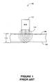
- FIG. 1 shows a typical ECS 110.
- a substrate 120 has a conductive film 130 or layer thereon and an EMF 112 emitted from the ECS 110 (not drawn to scale).
- the EMF 112 is considered to effectively penetrate through a conductor a depth quantity referred to as "a skin depth.”
- a skin depth is the distance into a target (e.g., a conductor), which an EMF wave will decay to about 1/e (about 37%) of the initial value of the EMF wave.
- Skin depth is a function of the frequency of the EMF 112 and the conductor material type and other factors. If the conductor is the conductive film 130 and the conductive film is copper, the skin depth is about 220,000 angstrom, at 1 MHz. If the copper film 130 is thinner than the skin depth (e.g. about 5000 angstrom), then the EMF 112 will induce an eddy current in both the copper film 130 and the substrate 120.
- the resulting signal that is detected by the ECS 110 includes components attributable to both an eddy current induced in the substrate 120 and an eddy current induced in the copper film 130.
- the EMF does not actually stop penetrating at skin depth as at least part (e.g., about 37%) of the EMF penetrates further beyond the conductor 130 (e.g., into the substrate 120 and the environment beyond the substrate 120).
- the conductor 130 is thinner than skin depth, a large portion of the EMF penetrates into and even through the substrate 120 a penetration distance 114.
- the substrate 120 offers significant resistivity, a very small eddy current is induced in the substrate 120.
- the majority e.g., about 90-95%) of the detected ECS signal is due to the eddy current induced into the conductor 130. Only about 5-10% of the detected ECS signal is due to the eddy current induced in the substrate 120.
- the resistivity of the silicon substrate 120 can vary from edge to center due to the varying physical characteristics (e.g., crystalline structure, dopant concentration, and other physical characteristics) of the crystal from which the substrate was cut. Because the resistivity varies, the eddy current in the silicon substrate 120 can also vary a proportional amount between the center and the edge of the substrate 120.
- a typical silicon substrate is identified is having an "average resistivity" value.
- the average resistivity value indicates that it is possible for the resistivity at the edge of the substrate 120 to be half the resistivity at the center of the substrate 120, resulting in a 100% or more variation in resistivity.
- a water can be labeled as having an average resistivity of 1.0 ohm/cm.
- a resistivity of 1.0 ohm/cm could allow a resistivity of 0.5 ohm/cm on the edge of the wafer and a resistivity of 1.5 ohm/cm or more at the center of the wafer, resulting in a variation of 300% or more between the edge and the center.
- Silicon substrates can also be labeled with a range of resistivity (e.g., 0.008 - 0.020 ohm/cm) indicating that the resistivity anywhere on the wafer will fall within the stated range.
- a range of 0.008 - 0.020 ohm/cm allows for a 250% variation in resistivity. Therefore, even if only about 5-10% of the detected ECS signal is due to the eddy current induced in the substrate, 120, the 5-10% can vary widely. By way of example, between about 2% and about 6% or between about 4% and about 10%.
- US 2002/149360 A1 discloses a method of measuring a thin film metal coating on wafer products by using eddy current technologies.
- the present invention provides methods and a system as set out in the claims.
- the present invention fills these needs by providing an improved system and method of measuring an ECS signal.
- One embodiment includes a method for determining a component of an eddy current sensor (ECS) signal attributable to a substrate.
- the method includes placing a substrate in a first position relative to an ECS at a first distance from the EGS.
- the substrate can include a conductive film on a first surface of the substrate.
- a first ECS signal can be detected with the substrate in the first position,
- the substrate can then be inverted relative to the EGS such that the substrate is in a second position relative to the ECS at a second distance from the ECS.
- the second distance is equal to the first distance less about a thickness of the substrate.
- a second ECS signal is detected with the substrate in the second position.
- a difference signal is determined.
- the difference signal is equal to a difference between a first signal level on a calibration graph for the ECS and the second signal level.
- the second signal level being shifted a distance about equal to the thickness of the substrate.
- a first substrate component of the first ECS signal is calculated.
- the first substrate component of the first ECS signal is equal to a product of the first distance and the difference signal, divided by the thickness of the substrate.
- the conductive film has a thickness of between about 10 and about 20,000 angstroms.
- the conductive film is a film residue.
- the ECS can be aligned with a first point in both the first position and the second position, the first point being on the first surface of the substrate.
- the conductive film is juxtaposed between the substrate and the ECS in the first position.
- Inverting the substrate can include moving the ECS.
- Inverting the substrate can include moving the substrate.
- Inverting the substrate can include adjusting the substrate an amount equal to about a thickness of the conductive film.
- the method can also include calculating a second substrate component of the second ECS signal.
- the second substrate component of the second ECS signal is equal to a product of the second distance and the difference signal, divided by the thickness of the substrate.
- the method can also include calculating a component of the first ECS signal attributable to the conductive film.
- the component of the first ECS signal attributable to the conductive film is equal to a difference between the first ECS signal and the first substrate component of the first ECS signal.
- a thickness the conductive film can also be determined.
- Another embodiment includes a method for mapping a resistivity of a substrate.
- the method includes determining a component of the eddy current sensor (ECS) signal attributable to the substrate relative to a first point and a second point on the surface of the substrate.
- a first resistivity is calculated for the first point and a second resistivity is calculated for the second point.
- a resistivity curve can be extrapolated from the resistivity at the first point and the second point.
- ECS eddy current sensor
- Another embodiment includes a system for determining a component of an eddy current sensor (ECS) signal attributable to a substrate.
- the system includes an ECS oriented toward a substrate.
- the substrate is in a first position relative to the ECS at a first distance from the ECS.
- the substrate includes a conductive film on a first surface of the substrate.
- a substrate inverter is also included.
- the substrate inverter is capable of inverting the substrate relative to the ECS such that the substrate is in a second position relative to the ECS at a second distance from the ECS.
- the second distance is equal to the first distance less about a thickness of the substrate.
- a control system is coupled to the ECS.
- the control system includes logic that detects a first ECS signal with the substrate in the first position and logic that detects a second ECS signal with the substrate in the second position.
- the control system also includes logic that determines a difference signal equal to a difference between a first signal level on a calibration graph for the ECS and the second signal level. The second signal level being shifted a distance about equal to the thickness of the substrate.
- the control system further includes logic that calculates a first substrate component of the first ECS signal equal to a product of the first distance and the difference signal, divided by the thickness of the substrate.
- the system can also include a stage for supporting the substrate in the first position and the second position.
- the stage can be adjustable to compensate for a thickness of the conductive film.
- the substrate inverter can include an end effector that can invert the substrate.
- the substrate inverter includes an actuator that moves the ECS.
- the ECS can also include a first ECS and a second ECS and wherein the substrate is in the first position relative to the first ECS and the substrate is in the second position relative to the second ECS.
- the first ECS and the second ECS are substantially aligned.
- the first distance can be substantially equal to the second distance.
- the first ECS and the second ECS are operated about 180 degrees out of phase.
- the present invention provides for more accurate measurement and detection of conductive films on a substrate and by accurately determining the resistivity of the substrate.
- Figure 1 shows a typical ECS.
- Figures 2A and 2B show a system for measuring the eddy current induced in a conductive film, in accordance with one embodiment of the present invention.
- Figure 3 is a flowchart of the method operations of determining a component of an ECS signal due to the eddy current induced into the substrate.
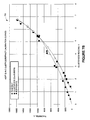
- Figure 4 shows a graph of the sensitivity of the ECS as compared to distance, in accordance with one embodiment of the present invention.
- Figure 5 is another system for determining a component of an ECS signal due to the eddy current induced into the substrate, in accordance with one embodiment of the present invention.
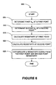
- Figure 6 is a flowchart of the method operations for mapping a resistivity of the substrate, in accordance with one embodiment of the present invention.
- Figure 7A is a graph of ECS signal data without correcting for the substrate contribution, in accordance with one embodiment of the present invention.
- Figure 7B is a graph of the same ECS signal data but with the substrate contribution being corrected or compensated for, in accordance with one embodiment of the present invention.
- conductive films e.g., copper films
- Thin film deposition and subsequent thin film measuring is becoming very common.
- Semiconductor wafers are typically submitted to a chemical mechanical planarizing (CMP) at at least one point in the semiconductor manufacturing process.
- CMP chemical mechanical planarizing
- Very thin, conductive film residues e.g., less than 1200 angstroms
- the very thin film residues must be accurately measured in both location and thickness so that the appropriate, additional CMP operation can be determined and applied to remove the residual film, without removing any excess material from below the residual film.
- An accurate measurement of a conductive film requires that the component of the ECS signal that is attributable to the eddy current in the substrate must be substantially eliminated, minimized or compensated for.
- Various approaches for substantially eliminating, minimizing or compensating for the ECS signal that is attributable to the substrate are described herein.
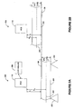
- FIGS 2A and 2B show a system 200 for measuring the eddy current induced in a conductive film 230, in accordance with one embodiment of the present invention.
- the system 200 includes an ECS 110, which is coupled to a controller 250 for controlling the ECS 110.
- a stage or substrate support 252 is also includes for supporting the substrate 220 at a known location.
- An end effector or other substrate handling system could also be included for moving and inverting the substrate 220.
- the system 200 can also include an actuator that can move the ECS 110. Referring first to Figure 2A , in which a semiconductor substrate 220, with the conductive film 230 thereon, is oriented in a first position, with the conductive film 230 nearest the ECS 110.
- the conductive film 230 can be between anywhere from a few angstroms to up to 20,000 angstroms or more.
- the conductive film 230 can be a very thin film residue (e.g., less than 1200 angstrom) such as what may remain after an incomplete CMP process.
- the semiconductor substrate 220 is typically about 750 ⁇ m (7,500,000 angstrom) in thickness.
- the ECS 110 is oriented a distance D s1 from a centerline 222 of the substrate 220.
- Distance D s1 is a known distance from the centerline 222.
- the distance D s1 can be determined by measuring an actual distance between the surface of the film and adding 375 ⁇ m, where 375 ⁇ m is equal to one half of the typical thickness of a typical semiconductor substrate 220 of about 750 ⁇ m.
- Figure 3 is a flowchart of the method operations 300 of determining a component of an ECS signal due to the eddy current induced into the substrate 220.
- the substrate 220 is placed in the first position.
- the ECS 110 induces an eddy current into the thin conductive film 230 and the substrate 220 and receives a first ECS signal S 1 .
- the first ECS signal S 1 is a sum of two component signals S s1 and S f .
- S s1 is the component due to the eddy current induced into the substrate 220 in the first position.
- S f is the ECS component due to the eddy current induced into the conductive film 230.
- the substrate 220 is moved to a second position as shown in Figure 2B .
- the conductive film 230 is in substantially the same location relative to the ECS 110 as in the first position, however, the semiconductor substrate 220 is juxtaposed between the conductive film 230 and the ECS 110.
- the substrate 220 is inverted with respect to the ECS 110, as compared to the first position.
- the location of the substrate 230 can be adjusted to correct for the shift (i.e. 2 ⁇ m) due to conductive film.
- the substrate 230 may not be adjusted because the component of the ECS signal attributable to the substrate 220 is only a very small portion (e.g., 5-10%) of the total ECS signal.
- An error in the distance D s2 between the substrate 220 and the ECS 110 of up to 10% is tolerable as will be described in more detail below.
- the conductive film 230 is in substantially the same location relative to the ECS 110 as in the first position, however, the semiconductor substrate 220 is juxtaposed between the conductive film 230 and the ECS 110.
- the ECS 110 could be moved to an opposite side of the substrate 220 such that the substrate 220 is inverted relative to the ECS 110.
- a distance D s2 is the distance between the centerline 222 and the ECS 110 with the substrate 220 in the second position.
- the ECS 110 is also oriented in the same location relative to a point (X, Y) on the surface of the substrate 220 in both the first position and the second position.
- the ECS 110 induces an eddy current into the conductive film 230 and the substrate 220 and receives a second ECS signal S 2 .
- the second ECS signal S 2 is a sum of two component signals S s2 and S f .
- S S2 is the ECS component due to the eddy current induced into the substrate 220 in the second position.
- S f is the ECS component due to the eddy current induced into the thin conductive film 230.
- S s1 and S s2 are different because the ECS signal is a function of the distance D s2 between the ECS 110 and the substrate 220.
- Distance D s2 is less than the distance D s1 .
- the difference between the D s1 and D s2 is equal to about the thickness of the substrate 220 (i.e., about 750 ⁇ m).
- a distance D f between the conductive film 230 and the ECS 110 is substantially the same in both the first position and the second position so therefore S f is substantially the same in both S 1 and S 2 .
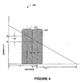
- Figure 4 shows a graph 400 of the sensitivity of the ECS 110 as compared to distance, in accordance with one embodiment of the present invention.
- the substrate 220 is shown in the first position 410 and then in the second position 420.
- ⁇ S is determined by referencing graph 400.
- the sensitivity of the ECS 110 is plotted on the ⁇ -axis and the distance between the ECS 110 and the detected conductor (e.g., substrate 220) is plotted on the x-axis. As the distance increases, the ECS signal approaches zero and as the distance approaches zero the ECS detects a maximum signal.
- the sensitivity graph 400 of the ECS is substantially linear.
- an eddy current target e.g., conductor 230 or substrate 220
- the sensitivity is equal to S d1 as shown on the graph 400.
- the eddy current target is moved 750 ⁇ m closer to the ECS 110, then sensitivity is equal to S d2 .
- the ⁇ S is a difference between S d1 and S d2 . Because the graph 400 is linear, then any shift of 750 ⁇ m along the x-axis results in a shift in the signal strength of the ECS signal equal to ⁇ S (i.e., the difference between S d1 and S d2 ) and therefore ⁇ S a known quantity from the calibration graph 400.
- the component of the ECS signal attributable to the substrate 220 (ECS ss ) is determined. Recall that as described in Figures 2A and 2B above, where the substrate 220 having a thickness of 750 ⁇ m, is moved 750 ⁇ m closer to the ECS 110 in the second position, than in the first position, then ⁇ S can be found on the calibration graph 400.
- a component of the first ECS signal attributable to the conductive film 230 (S f ) can be also be calculated.
- the thickness of the conductive film can be accurately determined by reference to a calibration table that plots ECS signal strength versus thickness of a conductive film of the same type as the conductive film 230.
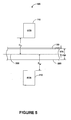
- FIG. 5 is another system 500 for determining a component of an ECS signal due to the eddy current induced into the substrate 220, in accordance with one embodiment of the present invention.
- the system 500 includes two ECS 110, 210 that are on opposite sides of the substrate 220.
- the two ECS 110, 210 can also be at substantially the different distances (i.e., D s1' ⁇ D s2' ) from the centerline 222 of the substrate 220.
- the two ECS 110, 210 are also substantially aligned with each other. Similar to as described in Figure 3 above, the substrate 220 is in a first position relative to the first ECS 110 while simultaneously, the substrate 220 is in a second position relative to the second ECS 110. In this system 500, the first and second ECS signals can be detected in very short succession and without physically inverting either the substrate 220 or the ECS 110, 210.
- the ECS 110, 210 can also be operated in a manner to increase the sensitivity of the detected ECS signals by operating the ECS 110, 210 simultaneously but 180 degrees out of phase.
- the first EMF from the first ECS 110 reflects the second EMF from the second ECS 210, which effectively amplifies the detected ECS signals such as described in commonly owned US Patent application 10/256,055 which was filed on September 25, 2002 , by Gotkis et. al and entitled "Enhancement of Eddy Current Based Measurement Capabilities," published after the priority date of the present application, eg. as US2004058545 or WO2004029606 .
- Figure 6 is a flowchart of the method operations 600 for mapping a resistivity of the substrate, in accordance with one embodiment of the present invention.
- a first component of the ECS signal attributable to the substrate 220 relative to a first point (first S s1 ) on the surface of the substrate is determined as described in the above-described methods.
- a second component of the ECS signal attributable to the substrate 220 relative to a second point (second S s1 ) on the surface of the substrate is determined.
- a first resistivity is calculated for the first point and in operation 620, a second resistivity is calculated for the second point.
- a resistivity curve can be extrapolated from the resistivity at the first point and the second point.
- a typical substrate has a substantially linear resistivity measured radially. Therefore if the first point and the second point have a different radius from the center of the substrate, then the resistivity curve can be extrapolated from the two points.
- Figures 7A and 7B are graphs 700, 750 of ECS signals in accordance with one embodiment of the present invention.
- Figure 7A is a graph 700 of ECS signal data without correcting for the substrate contribution, in accordance with one embodiment of the present invention.
- Figure 7B is a graph 750 of the same ECS signal data but with the substrate contribution being corrected or compensated for, in accordance with one embodiment of the present invention.
- the "film only" curve 750 starts very close to 0,0 center of coordinates. As can be readily seen, identifying and compensating for the substrate contribution in an ECS signal allows for a true "thin film only" device calibration.
- the term "about” means +/- 10%.
- the phrase "about 750 ⁇ m” indicates a range of between 675 ⁇ m and 825 ⁇ m.
- the invention may employ various computer-implemented operations involving data stored in computer systems. These operations are those requiring physical manipulation of physical quantities. Usually, though not necessarily, these quantities take the form of electrical or magnetic signals capable of being stored, transferred, combined, compared, and otherwise manipulated. Further, the manipulations performed are often referred to in terms, such as producing, identifying, determining, or comparing.
- the invention also relates to a device or an apparatus for performing these operations.
- the apparatus may be specially constructed for the required purposes, or it may be a general-purpose computer selectively activated or configured by a computer program stored in the computer.
- various general-purpose machines may be used with computer programs written in accordance with the teachings herein, or it may be more convenient to construct a more specialized apparatus to perform the required operations.
- the invention can also be embodied as computer readable code on a computer readable medium.
- the computer readable medium is any data storage device that can store data which can be thereafter be read by a computer system. Examples of the computer readable medium include hard drives, network attached storage (NAS), read-only memory, random-access memory, CD-ROMs, CD-Rs, CD-RWs, magnetic tapes, and other optical and non-optical data storage devices.
- the computer readable medium can also be distributed over a network coupled computer systems so that the computer readable code is stored and executed in a distributed fashion.
Landscapes
- Physics & Mathematics (AREA)
- General Physics & Mathematics (AREA)
- Chemical & Material Sciences (AREA)
- Chemical Kinetics & Catalysis (AREA)
- Electrochemistry (AREA)
- Health & Medical Sciences (AREA)
- Life Sciences & Earth Sciences (AREA)
- Analytical Chemistry (AREA)
- Biochemistry (AREA)
- General Health & Medical Sciences (AREA)
- Immunology (AREA)
- Pathology (AREA)
- Measurement Of Length, Angles, Or The Like Using Electric Or Magnetic Means (AREA)
Claims (20)
- Verfahren zum Bestimmen einer Komponente eines Wirbelstromsensor-, ECS, -signals, das einem Substrat (220) zuzurechnen ist, umfassend:Platzieren eines Substrats (220) in einer ersten Position relativ zu einem ECS (110) in einem ersten Abstand vom ECS (110), wobei das Substrat (220) eine leitende Schicht (230) auf einer ersten Oberfläche des Substrats (220) beinhaltet;Erfassen eines ersten ECS-Signals mit dem Substrat (220) in der ersten Position;Invertieren des Substrats (220) relativ zum ECS (110), so dass das Substrat (220) sich in einer zweiten Position relativ zum ECS (110) in einem zweiten Abstand vom ECS (110) befindet, wobei der zweite Abstand gleich dem ersten Abstand beträgt, der weniger als ungefähr eine Dicke des Substrats (220) ist;Erfassen eines zweiten ECS-Signals mit dem Substrat (220) in der zweiten Position;Bestimmen eines Differenzsignals, das gleich einer Differenz zwischen einem ersten Signalpegel auf einer Eichkurve für den ECS (110) und dem zweiten Signalpegel ist, wobei der zweite Signalpegel um einen Abstand versetzt wird, der ungefähr gleich der Dicke des Substrats (220) ist; undBerechnen einer ersten Substratkomponente des ersten ECS-Signals, das gleich einem Produkt des ersten Abstands und des Differenzsignals, geteilt durch die Dicke des Substrats (220), ist.
- Verfahren nach Anspruch 1, wobei die leitende Schicht (230) eine Dicke zwischen ungefähr 10 und ungefähr 20.000 Angström hat.
- Verfahren nach Anspruch 1, wobei die leitende Schicht (230) ein Schichtrest ist.
- Verfahren nach Anspruch 1, wobei der ECS (110) mit einem ersten Punkt sowohl an der ersten Position als auch der zweiten Position ausgerichtet ist, wobei sich der erste Punkt auf der ersten Oberfläche des Substrats (220) befindet.
- Verfahren nach Anspruch 1, wobei die leitende Schicht (230) zwischen dem Substrat (220) und dem ECS (110) in der ersten Position nebeneinander gelegt ist.
- Verfahren nach Anspruch 1, wobei das Invertieren des Substrats (220) das Bewegen des ECS (110) beinhaltet.
- Verfahren nach Anspruch 1, wobei das Invertieren des Substrats (220) das Bewegen des Substrats (220) beinhaltet.
- Verfahren nach Anspruch 1, wobei das Invertieren des Substrats (220) das Verstellen des Substrats (220) um einen Betrag beinhaltet, der gleich ungefähr einer Dicke der leitenden Schicht (230) ist.
- Verfahren nach Anspruch 1, weiterhin umfassend das Berechnen einer zweiten Substratkomponente des zweiten ECS-Signals, das gleich einem Produkt des zweiten Abstands und des Differenzsignals, geteilt durch die Dicke des Substrats (220), ist.
- Verfahren nach Anspruch 1, weiterhin umfassend:Berechnen einer Komponente des ersten ECS-Signals, das der leitenden Schicht (230) zuzurechnen ist, die gleich einer Differenz zwischen dem ersten ECS-Signal und der ersten Substratkomponente des ersten ECS-Signals ist.
- Verfahren nach Anspruch 10, weiterhin umfassend das Bestimmen einer Dicke der leitenden Schicht (230).
- Verfahren zum Kartieren des spezifischen Widerstands eines Substrats (220), umfassend:Bestimmen einer Komponente des Wirbelstromsensor-, ECS, -signals, das einem Substrat (230) relativ zu einem ersten Punkt auf der Oberfläche des Substrats (220) zuzurechnen ist, einschließlich:Platzieren eines Substrats (220) in einer ersten Position relativ zu einem ECS (110) in einem ersten Abstand vom ECS (110), wobei das Substrat (220) eine leitende Schicht (230) auf einer ersten Oberfläche des Substrats (220) beinhaltet;Erfassen eines ersten ECS-Signals mit dem Substrat (220) in der ersten Position;Invertieren des Substrats (220) relativ zum ECS (110) so, dass sich das Substrat (220) in einer zweiten Position relativ zum ECS (110) in einem zweiten Abstand vom ECS (110) befindet, wobei der zweite Abstand, der gleich dem ersten Abstand ist, weniger als ungefähr eine Dicke des Substrats (220) beträgt;Erfassen eines zweiten ECS-Signals mit dem Substrat (220) in der zweiten Position;Bestimmen eines Differenzsignals, das gleich einer Differenz zwischen einem ersten Signalpegel auf einer Eichkurve für den ECS (110) und dem zweiten Signalpegel ist, wobei der zweite Signalpegel um einen Abstand versetzt wird, der ungefähr gleich der Dicke des Substrats (220) ist; undBerechnen einer ersten Substratkomponente des ersten ECS-Signals, das gleich einem Produkt des ersten Abstands und des Differenzsignals, geteilt durch die Dicke des Substrats (220), ist;Bestimmen einer Komponente des Wirbelstromsensor-ECS-Signals, das einem Substrat (220) relativ zu einem zweiten Punkt auf der Oberfläche des Substrats (220) zuzurechnen ist;Berechnen eines ersten spezifischen Widerstands am ersten Punkt; Berechnen eines zweiten spezifischen Widerstands am zweiten Punkt; undExtrapolieren einer spezifischen Widerstandskurve aus dem spezifischen Widerstand am ersten Punkt und zweiten Punkt.
- System (200) zum Bestimmen einer Komponente eines Wirbelstromsensor-, ECS, -signals, das einem Substrat (220) zuzurechnen ist, umfassend:einen ECS (110), der in Richtung eines Substrats (220) ausgerichtet ist, wobei sich das Substrat (220) in einer ersten Position relativ zum ECS (110) in einem ersten Abstand vom ECS (110) befindet, wobei das Substrat (220) eine leitende Schicht (230) auf einer ersten Oberfläche des Substrats (220) beinhaltet;einen Substratwechselrichter, der imstande ist, das Substrat (220) relativ zum ECS (110) so zu invertieren, dass das Substrat (220) sich in einer zweiten Position relativ zum ECS (110) in einem zweiten Abstand vom ECS (110) befindet, wobei der zweite Abstand, der gleich dem ersten Abstand ist, weniger als ungefähr eine Dicke des Substrats (220) beträgt;ein mit dem ECS (110) gekoppeltes Steuersystem, wobei das Steuersystem einschließt:eine Logik, die ein erstes ECS-Signal mit dem Substrat (220) in der ersten Position erfasst;eine Logik, die ein zweites ECS-Signal mit dem Substrat (220) in der zweiten Position umfasst;eine Logik, die ein Differenzsignal bestimmt, das gleich einer Differenz zwischen einem ersten Signalpegel auf einer Kalibrierungskurve für den ECS und dem zweiten Signalpegel ist, wobei der zweite Signalpegel um einen Abstand versetzt wird, der ungefähr gleich der Dicke des Substrats (220) ist; undeine Logik, die eine erste Substratkomponente des ersten ECS-Signals berechnet, das gleich einem Produkt des ersten Abstands und des Differenzsignals, geteilt durch die Dicke des Substrats (220), ist.
- System (200) nach Anspruch 13, weiterhin umfassend ein Gestell zum Stützen des Substrats (220) in der ersten Position und der zweiten Position.
- System (200) nach Anspruch 14, wobei das Gestell verstellbar ist, um eine Dicke der leitenden Schicht (230) zu kompensieren.
- System (200) nach Anspruch 13, wobei der Substratwechselrichter ein Greiforgan beinhaltet, das das Substrat (220) invertieren kann.
- System (200) nach Anspruch 13, wobei der Substratwechselrichter einen Aktor beinhaltet, der den ECS (110) bewegt.
- System (200) nach Anspruch 13, wobei der ECS (110) einen ersten ECS und einen zweiten ECS beinhaltet und wobei das Substrat (220) in der ersten Position relativ zum ersten ECS ist und das Substrat (220) in der zweiten Position relativ zum zweiten ECS ist, und wobei der erste ECS und der zweite ECS im Wesentlichen ausgerichtet sind.
- System (200) nach Anspruch 18, wobei der erste Abstand im Wesentlichen gleich dem zweiten Abstand ist.
- System (200) nach Anspruch 18, wobei der erste ECS und der zweite ECS um ungefähr 180° phasenverschoben betrieben werden.
Applications Claiming Priority (3)
| Application Number | Priority Date | Filing Date | Title |
|---|---|---|---|
| US328912 | 1994-10-25 | ||
| US10/328,912 US6788050B2 (en) | 2002-12-23 | 2002-12-23 | System, method and apparatus for thin-film substrate signal separation using eddy current |
| PCT/US2003/041084 WO2004059313A1 (en) | 2002-12-23 | 2003-12-22 | System, method and apparatus for thin-film substrate signal separation using eddy current |
Publications (3)
| Publication Number | Publication Date |
|---|---|
| EP1576362A1 EP1576362A1 (de) | 2005-09-21 |
| EP1576362A4 EP1576362A4 (de) | 2011-03-16 |
| EP1576362B1 true EP1576362B1 (de) | 2012-04-04 |
Family
ID=32594619
Family Applications (1)
| Application Number | Title | Priority Date | Filing Date |
|---|---|---|---|
| EP03800121A Expired - Lifetime EP1576362B1 (de) | 2002-12-23 | 2003-12-22 | System, verfahren und vorrichtung zur dünnfilmsubstrat-signaltrennung unter verwendung von wirbelströmen |
Country Status (8)
| Country | Link |
|---|---|
| US (1) | US6788050B2 (de) |
| EP (1) | EP1576362B1 (de) |
| JP (1) | JP4368309B2 (de) |
| KR (1) | KR101051909B1 (de) |
| CN (2) | CN1732384A (de) |
| AU (1) | AU2003299847A1 (de) |
| TW (1) | TWI230258B (de) |
| WO (1) | WO2004059313A1 (de) |
Families Citing this family (10)
| Publication number | Priority date | Publication date | Assignee | Title |
|---|---|---|---|---|
| US7242185B1 (en) * | 2005-03-30 | 2007-07-10 | Lam Research Corporation | Method and apparatus for measuring a conductive film at the edge of a substrate |
| GB2470779A (en) * | 2009-06-05 | 2010-12-08 | Monitran Ltd | Eddy current proximity probe system and method of measuring that mitigates errors due to temperature fluctuations |
| DE102012215897A1 (de) * | 2012-09-07 | 2014-03-13 | Robert Bosch Gmbh | Schallwandlervorrichtung und Verfahren zum Herstellen derselben, Sensorvorrichtung und Verfahren zum Bestimmen eines akustischen Signals |
| WO2015047374A1 (en) | 2013-09-30 | 2015-04-02 | Rinand Solutions Llc | Operating multiple functions in a display of an electronic device |
| US9726922B1 (en) | 2013-12-20 | 2017-08-08 | Apple Inc. | Reducing display noise in an electronic device |
| US10296123B2 (en) | 2015-03-06 | 2019-05-21 | Apple Inc. | Reducing noise in a force signal in an electronic device |
| US10185397B2 (en) * | 2015-03-08 | 2019-01-22 | Apple Inc. | Gap sensor for haptic feedback assembly |
| KR101635086B1 (ko) | 2015-05-29 | 2016-06-30 | 삼성중공업 주식회사 | 머드 탱크 및 이를 포함하는 선박 |
| US9927905B2 (en) | 2015-08-19 | 2018-03-27 | Apple Inc. | Force touch button emulation |
| US10416811B2 (en) | 2015-09-24 | 2019-09-17 | Apple Inc. | Automatic field calibration of force input sensors |
Family Cites Families (23)
| Publication number | Priority date | Publication date | Assignee | Title |
|---|---|---|---|---|
| DE2049976B2 (de) * | 1970-10-12 | 1972-09-21 | Elektro-Physik Hans Nix & Dr.-Ing. E. Steingroever KG, 5000 Köln | Verfahren zur messung der dicke von schichten im bauwesen und vorrichtung zur durchfuehrung des verfahren |
| US4556845A (en) | 1982-05-17 | 1985-12-03 | International Business Machines Corporation | Method for monitoring deposition rate using an eddy current detector |
| JPS59104545A (ja) * | 1982-12-07 | 1984-06-16 | Kobe Steel Ltd | 連続鋳造鋼片の熱間探傷方法 |
| JPS6138503A (ja) * | 1984-07-31 | 1986-02-24 | Ketsuto Kagaku Kenkyusho:Kk | 膜厚計 |
| JPS6166104A (ja) * | 1984-09-07 | 1986-04-04 | Anelva Corp | 金属薄膜膜厚測定方法 |
| JPH01257203A (ja) * | 1988-04-07 | 1989-10-13 | Sumitomo Metal Ind Ltd | 電気めっき方法及び装置 |
| JPH0784676B2 (ja) * | 1989-05-16 | 1995-09-13 | 三菱自動車工業株式会社 | 防錆鋼板判別装置 |
| US5017869A (en) * | 1989-12-14 | 1991-05-21 | General Electric Company | Swept frequency eddy current system for measuring coating thickness |
| US5485082A (en) * | 1990-04-11 | 1996-01-16 | Micro-Epsilon Messtechnik Gmbh & Co. Kg | Method of calibrating a thickness measuring device and device for measuring or monitoring the thickness of layers, tapes, foils, and the like |
| JPH04147004A (ja) * | 1990-10-11 | 1992-05-20 | Ichikoh Ind Ltd | 車両用外装品の塗装膜厚さ寸法の測定方法 |
| US5473247A (en) * | 1993-04-06 | 1995-12-05 | Magnetic Analysis Corporation | Apparatus for discriminating defects in top and bottom surfaces of objects |
| US5559428A (en) | 1995-04-10 | 1996-09-24 | International Business Machines Corporation | In-situ monitoring of the change in thickness of films |
| SE508354C2 (sv) | 1996-07-05 | 1998-09-28 | Asea Atom Ab | Förfarande och anordning för bestämning av skikttjocklek |
| JP2002533659A (ja) * | 1998-12-18 | 2002-10-08 | マイクロ−エプシロン・メステヒニク・ゲーエムベーハー・ウント・コンパニー・カー・ゲー | 渦電流センサの作動方法及び渦電流センサ |
| JP4292612B2 (ja) * | 1999-02-09 | 2009-07-08 | 東洋紡績株式会社 | 表面抵抗測定装置 |
| EP1244907A1 (de) * | 1999-12-23 | 2002-10-02 | KLA-Tencor Corporation | Vor-ort-überwachung für metallisationsprozesse unter verwendung von wirbelstrommessungen und optischen messungen |
| JP4874465B2 (ja) * | 2000-03-28 | 2012-02-15 | 株式会社東芝 | 渦電流損失測定センサ |
| US6549006B2 (en) * | 2000-04-07 | 2003-04-15 | Cuong Duy Le | Eddy current measurements of thin-film metal coatings using a selectable calibration standard |
| DE60116757D1 (de) * | 2000-05-19 | 2006-04-06 | Applied Materials Inc | Verfahren und vorrichtung zur "in-situ" überwachung der dicke während des chemisch-mechanischen planiervorganges |
| JP3854083B2 (ja) * | 2000-10-12 | 2006-12-06 | 株式会社荏原製作所 | 半導体基板製造装置 |
| TW541425B (en) | 2000-10-20 | 2003-07-11 | Ebara Corp | Frequency measuring device, polishing device using the same and eddy current sensor |
| JP2002148012A (ja) * | 2000-11-08 | 2002-05-22 | Ulvac Japan Ltd | 膜厚測定装置及び膜厚測定方法 |
| US7084621B2 (en) * | 2002-09-25 | 2006-08-01 | Lam Research Corporation | Enhancement of eddy current based measurement capabilities |
-
2002
- 2002-12-23 US US10/328,912 patent/US6788050B2/en not_active Expired - Lifetime
-
2003
- 2003-12-22 EP EP03800121A patent/EP1576362B1/de not_active Expired - Lifetime
- 2003-12-22 CN CNA2003801074074A patent/CN1732384A/zh active Pending
- 2003-12-22 KR KR1020057011911A patent/KR101051909B1/ko not_active Expired - Fee Related
- 2003-12-22 AU AU2003299847A patent/AU2003299847A1/en not_active Abandoned
- 2003-12-22 CN CN201110111352.0A patent/CN102269566B/zh not_active Expired - Lifetime
- 2003-12-22 WO PCT/US2003/041084 patent/WO2004059313A1/en not_active Ceased
- 2003-12-22 JP JP2004563995A patent/JP4368309B2/ja not_active Expired - Fee Related
- 2003-12-23 TW TW092136542A patent/TWI230258B/zh not_active IP Right Cessation
Also Published As
| Publication number | Publication date |
|---|---|
| AU2003299847A1 (en) | 2004-07-22 |
| JP4368309B2 (ja) | 2009-11-18 |
| US6788050B2 (en) | 2004-09-07 |
| WO2004059313A1 (en) | 2004-07-15 |
| CN1732384A (zh) | 2006-02-08 |
| CN102269566B (zh) | 2014-05-14 |
| EP1576362A4 (de) | 2011-03-16 |
| EP1576362A1 (de) | 2005-09-21 |
| JP2006511805A (ja) | 2006-04-06 |
| TWI230258B (en) | 2005-04-01 |
| CN102269566A (zh) | 2011-12-07 |
| TW200420880A (en) | 2004-10-16 |
| KR20050088469A (ko) | 2005-09-06 |
| KR101051909B1 (ko) | 2011-07-26 |
| US20040119469A1 (en) | 2004-06-24 |
Similar Documents
| Publication | Publication Date | Title |
|---|---|---|
| US5625170A (en) | Precision weighing to monitor the thickness and uniformity of deposited or etched thin film | |
| EP1576362B1 (de) | System, verfahren und vorrichtung zur dünnfilmsubstrat-signaltrennung unter verwendung von wirbelströmen | |
| US6654698B2 (en) | Systems and methods for calibrating integrated inspection tools | |
| US20030210041A1 (en) | Eddy current measuring system for monitoring and controlling a chemical vapor deposition (CVD) process | |
| US6741076B2 (en) | Eddy current measuring system for monitoring and controlling a CMP process | |
| US7128803B2 (en) | Integration of sensor based metrology into semiconductor processing tools | |
| US6549006B2 (en) | Eddy current measurements of thin-film metal coatings using a selectable calibration standard | |
| US7112961B2 (en) | Method and apparatus for dynamically measuring the thickness of an object | |
| US6762604B2 (en) | Standalone eddy current measuring system for thickness estimation of conductive films | |
| WO2001046684A1 (en) | In-situ metalization monitoring using eddy current measurements and optical measurements | |
| WO2001084075A1 (en) | Methods for sensing positions of an actuator moving longitudinally | |
| US5341678A (en) | Method for determining thickness of ferromagnetic material deposition on nuclear fuel rods | |
| EP0690488A2 (de) | Echt-Zeit-Messung der Ätzate während eines chemischen Ätzverfahrens | |
| US7005306B1 (en) | Accurate thickness measurement of thin conductive film | |
| US7282909B2 (en) | Methods and apparatus for determining the thickness of a conductive layer on a substrate | |
| US6951503B1 (en) | System and method for in-situ measuring and monitoring CMP polishing pad thickness | |
| TWI401757B (zh) | 用於最佳化對基板上的一組導電層之電響應的方法與設備 | |
| CN1739002A (zh) | 在两个涡流传感头之间测量待测物厚度的方法和装置 | |
| US20040070393A1 (en) | Differential measurement method using eddy-current sensing to resolve a stack of conducting films on substrates | |
| US20030206008A1 (en) | Eddy current measuring system for monitoring and controlling a physical vapor deposition(PVD) process | |
| US20030206009A1 (en) | Integrated eddy current measuring system for monitoring and controlling multiple semiconductor wafer fabrication processes | |
| JPH02124406A (ja) | 半導体製造装置 | |
| US20040080326A1 (en) | Device and method for determining the sheet resistance of samples | |
| CN101435104A (zh) | 根据氮化硅薄膜应力校准薄膜沉积机台中机械手位置的方法 | |
| CN118884049B (zh) | 一种非接触式电阻率测量方法及系统 |
Legal Events
| Date | Code | Title | Description |
|---|---|---|---|
| PUAI | Public reference made under article 153(3) epc to a published international application that has entered the european phase |
Free format text: ORIGINAL CODE: 0009012 |
|
| 17P | Request for examination filed |
Effective date: 20050617 |
|
| AK | Designated contracting states |
Kind code of ref document: A1 Designated state(s): AT BE BG CH CY CZ DE DK EE ES FI FR GB GR HU IE IT LI LU MC NL PT RO SE SI SK TR |
|
| AX | Request for extension of the european patent |
Extension state: AL LT LV MK |
|
| DAX | Request for extension of the european patent (deleted) | ||
| RBV | Designated contracting states (corrected) |
Designated state(s): BE DE FR IT NL |
|
| A4 | Supplementary search report drawn up and despatched |
Effective date: 20110211 |
|
| RIC1 | Information provided on ipc code assigned before grant |
Ipc: G01B 7/06 20060101ALI20110207BHEP Ipc: G01N 27/72 20060101AFI20040720BHEP |
|
| 17Q | First examination report despatched |
Effective date: 20110615 |
|
| GRAP | Despatch of communication of intention to grant a patent |
Free format text: ORIGINAL CODE: EPIDOSNIGR1 |
|
| GRAS | Grant fee paid |
Free format text: ORIGINAL CODE: EPIDOSNIGR3 |
|
| GRAA | (expected) grant |
Free format text: ORIGINAL CODE: 0009210 |
|
| AK | Designated contracting states |
Kind code of ref document: B1 Designated state(s): BE DE FR IT NL |
|
| REG | Reference to a national code |
Ref country code: DE Ref legal event code: R096 Ref document number: 60340520 Country of ref document: DE Effective date: 20120524 |
|
| REG | Reference to a national code |
Ref country code: NL Ref legal event code: VDEP Effective date: 20120404 |
|
| PG25 | Lapsed in a contracting state [announced via postgrant information from national office to epo] |
Ref country code: BE Free format text: LAPSE BECAUSE OF FAILURE TO SUBMIT A TRANSLATION OF THE DESCRIPTION OR TO PAY THE FEE WITHIN THE PRESCRIBED TIME-LIMIT Effective date: 20120404 |
|
| PG25 | Lapsed in a contracting state [announced via postgrant information from national office to epo] |
Ref country code: NL Free format text: LAPSE BECAUSE OF FAILURE TO SUBMIT A TRANSLATION OF THE DESCRIPTION OR TO PAY THE FEE WITHIN THE PRESCRIBED TIME-LIMIT Effective date: 20120404 |
|
| PLBE | No opposition filed within time limit |
Free format text: ORIGINAL CODE: 0009261 |
|
| STAA | Information on the status of an ep patent application or granted ep patent |
Free format text: STATUS: NO OPPOSITION FILED WITHIN TIME LIMIT |
|
| PG25 | Lapsed in a contracting state [announced via postgrant information from national office to epo] |
Ref country code: IT Free format text: LAPSE BECAUSE OF FAILURE TO SUBMIT A TRANSLATION OF THE DESCRIPTION OR TO PAY THE FEE WITHIN THE PRESCRIBED TIME-LIMIT Effective date: 20120404 |
|
| 26N | No opposition filed |
Effective date: 20130107 |
|
| PGFP | Annual fee paid to national office [announced via postgrant information from national office to epo] |
Ref country code: FR Payment date: 20130110 Year of fee payment: 10 |
|
| PGFP | Annual fee paid to national office [announced via postgrant information from national office to epo] |
Ref country code: DE Payment date: 20121231 Year of fee payment: 10 |
|
| REG | Reference to a national code |
Ref country code: DE Ref legal event code: R097 Ref document number: 60340520 Country of ref document: DE Effective date: 20130107 |
|
| REG | Reference to a national code |
Ref country code: DE Ref legal event code: R119 Ref document number: 60340520 Country of ref document: DE |
|
| REG | Reference to a national code |
Ref country code: FR Ref legal event code: ST Effective date: 20140829 |
|
| REG | Reference to a national code |
Ref country code: DE Ref legal event code: R119 Ref document number: 60340520 Country of ref document: DE Effective date: 20140701 |
|
| PG25 | Lapsed in a contracting state [announced via postgrant information from national office to epo] |
Ref country code: DE Free format text: LAPSE BECAUSE OF NON-PAYMENT OF DUE FEES Effective date: 20140701 |
|
| PG25 | Lapsed in a contracting state [announced via postgrant information from national office to epo] |
Ref country code: FR Free format text: LAPSE BECAUSE OF NON-PAYMENT OF DUE FEES Effective date: 20131231 |