EP1573327B1 - Dna chip comprising a microarray made of microelectrode systems - Google Patents
Dna chip comprising a microarray made of microelectrode systems Download PDFInfo
- Publication number
- EP1573327B1 EP1573327B1 EP03795750.3A EP03795750A EP1573327B1 EP 1573327 B1 EP1573327 B1 EP 1573327B1 EP 03795750 A EP03795750 A EP 03795750A EP 1573327 B1 EP1573327 B1 EP 1573327B1
- Authority
- EP
- European Patent Office
- Prior art keywords
- electrodes
- electrode
- dna chip
- chip according
- sensor
- Prior art date
- Legal status (The legal status is an assumption and is not a legal conclusion. Google has not performed a legal analysis and makes no representation as to the accuracy of the status listed.)
- Expired - Lifetime
Links
- 238000002493 microarray Methods 0.000 title claims description 5
- 239000012491 analyte Substances 0.000 claims description 34
- 230000010287 polarization Effects 0.000 claims description 34
- 238000000018 DNA microarray Methods 0.000 claims description 33
- 238000006243 chemical reaction Methods 0.000 claims description 21
- 239000010409 thin film Substances 0.000 claims description 11
- 238000005516 engineering process Methods 0.000 claims description 9
- 238000001514 detection method Methods 0.000 claims description 7
- 239000000758 substrate Substances 0.000 claims description 7
- XUIMIQQOPSSXEZ-UHFFFAOYSA-N Silicon Chemical compound [Si] XUIMIQQOPSSXEZ-UHFFFAOYSA-N 0.000 claims description 4
- 229910052710 silicon Inorganic materials 0.000 claims description 4
- 239000010703 silicon Substances 0.000 claims description 4
- 239000000017 hydrogel Substances 0.000 claims description 3
- 230000002596 correlated effect Effects 0.000 claims description 2
- 230000005672 electromagnetic field Effects 0.000 claims description 2
- 238000005259 measurement Methods 0.000 description 19
- 238000000034 method Methods 0.000 description 14
- 230000008569 process Effects 0.000 description 7
- 230000008859 change Effects 0.000 description 6
- 230000000694 effects Effects 0.000 description 6
- 230000003071 parasitic effect Effects 0.000 description 6
- 239000004065 semiconductor Substances 0.000 description 5
- 230000002349 favourable effect Effects 0.000 description 4
- 238000010276 construction Methods 0.000 description 3
- 230000000875 corresponding effect Effects 0.000 description 3
- 238000013461 design Methods 0.000 description 3
- VYPSYNLAJGMNEJ-UHFFFAOYSA-N Silicium dioxide Chemical compound O=[Si]=O VYPSYNLAJGMNEJ-UHFFFAOYSA-N 0.000 description 2
- 230000002411 adverse Effects 0.000 description 2
- 238000004458 analytical method Methods 0.000 description 2
- 230000015572 biosynthetic process Effects 0.000 description 2
- 230000001351 cycling effect Effects 0.000 description 2
- 239000003792 electrolyte Substances 0.000 description 2
- 239000010408 film Substances 0.000 description 2
- 230000003647 oxidation Effects 0.000 description 2
- 238000007254 oxidation reaction Methods 0.000 description 2
- 230000009467 reduction Effects 0.000 description 2
- 230000035945 sensitivity Effects 0.000 description 2
- 238000000926 separation method Methods 0.000 description 2
- 229910052814 silicon oxide Inorganic materials 0.000 description 2
- 239000000126 substance Substances 0.000 description 2
- 108091034117 Oligonucleotide Proteins 0.000 description 1
- JLCPHMBAVCMARE-UHFFFAOYSA-N [3-[[3-[[3-[[3-[[3-[[3-[[3-[[3-[[3-[[3-[[3-[[5-(2-amino-6-oxo-1H-purin-9-yl)-3-[[3-[[3-[[3-[[3-[[3-[[5-(2-amino-6-oxo-1H-purin-9-yl)-3-[[5-(2-amino-6-oxo-1H-purin-9-yl)-3-hydroxyoxolan-2-yl]methoxy-hydroxyphosphoryl]oxyoxolan-2-yl]methoxy-hydroxyphosphoryl]oxy-5-(5-methyl-2,4-dioxopyrimidin-1-yl)oxolan-2-yl]methoxy-hydroxyphosphoryl]oxy-5-(6-aminopurin-9-yl)oxolan-2-yl]methoxy-hydroxyphosphoryl]oxy-5-(6-aminopurin-9-yl)oxolan-2-yl]methoxy-hydroxyphosphoryl]oxy-5-(6-aminopurin-9-yl)oxolan-2-yl]methoxy-hydroxyphosphoryl]oxy-5-(6-aminopurin-9-yl)oxolan-2-yl]methoxy-hydroxyphosphoryl]oxyoxolan-2-yl]methoxy-hydroxyphosphoryl]oxy-5-(5-methyl-2,4-dioxopyrimidin-1-yl)oxolan-2-yl]methoxy-hydroxyphosphoryl]oxy-5-(4-amino-2-oxopyrimidin-1-yl)oxolan-2-yl]methoxy-hydroxyphosphoryl]oxy-5-(5-methyl-2,4-dioxopyrimidin-1-yl)oxolan-2-yl]methoxy-hydroxyphosphoryl]oxy-5-(5-methyl-2,4-dioxopyrimidin-1-yl)oxolan-2-yl]methoxy-hydroxyphosphoryl]oxy-5-(6-aminopurin-9-yl)oxolan-2-yl]methoxy-hydroxyphosphoryl]oxy-5-(6-aminopurin-9-yl)oxolan-2-yl]methoxy-hydroxyphosphoryl]oxy-5-(4-amino-2-oxopyrimidin-1-yl)oxolan-2-yl]methoxy-hydroxyphosphoryl]oxy-5-(4-amino-2-oxopyrimidin-1-yl)oxolan-2-yl]methoxy-hydroxyphosphoryl]oxy-5-(4-amino-2-oxopyrimidin-1-yl)oxolan-2-yl]methoxy-hydroxyphosphoryl]oxy-5-(6-aminopurin-9-yl)oxolan-2-yl]methoxy-hydroxyphosphoryl]oxy-5-(4-amino-2-oxopyrimidin-1-yl)oxolan-2-yl]methyl [5-(6-aminopurin-9-yl)-2-(hydroxymethyl)oxolan-3-yl] hydrogen phosphate Polymers Cc1cn(C2CC(OP(O)(=O)OCC3OC(CC3OP(O)(=O)OCC3OC(CC3O)n3cnc4c3nc(N)[nH]c4=O)n3cnc4c3nc(N)[nH]c4=O)C(COP(O)(=O)OC3CC(OC3COP(O)(=O)OC3CC(OC3COP(O)(=O)OC3CC(OC3COP(O)(=O)OC3CC(OC3COP(O)(=O)OC3CC(OC3COP(O)(=O)OC3CC(OC3COP(O)(=O)OC3CC(OC3COP(O)(=O)OC3CC(OC3COP(O)(=O)OC3CC(OC3COP(O)(=O)OC3CC(OC3COP(O)(=O)OC3CC(OC3COP(O)(=O)OC3CC(OC3COP(O)(=O)OC3CC(OC3COP(O)(=O)OC3CC(OC3COP(O)(=O)OC3CC(OC3COP(O)(=O)OC3CC(OC3COP(O)(=O)OC3CC(OC3CO)n3cnc4c(N)ncnc34)n3ccc(N)nc3=O)n3cnc4c(N)ncnc34)n3ccc(N)nc3=O)n3ccc(N)nc3=O)n3ccc(N)nc3=O)n3cnc4c(N)ncnc34)n3cnc4c(N)ncnc34)n3cc(C)c(=O)[nH]c3=O)n3cc(C)c(=O)[nH]c3=O)n3ccc(N)nc3=O)n3cc(C)c(=O)[nH]c3=O)n3cnc4c3nc(N)[nH]c4=O)n3cnc4c(N)ncnc34)n3cnc4c(N)ncnc34)n3cnc4c(N)ncnc34)n3cnc4c(N)ncnc34)O2)c(=O)[nH]c1=O JLCPHMBAVCMARE-UHFFFAOYSA-N 0.000 description 1
- 238000013459 approach Methods 0.000 description 1
- 238000003491 array Methods 0.000 description 1
- 238000012742 biochemical analysis Methods 0.000 description 1
- 238000009933 burial Methods 0.000 description 1
- 239000003990 capacitor Substances 0.000 description 1
- 230000000295 complement effect Effects 0.000 description 1
- 230000001276 controlling effect Effects 0.000 description 1
- 238000005260 corrosion Methods 0.000 description 1
- 230000007797 corrosion Effects 0.000 description 1
- 230000008878 coupling Effects 0.000 description 1
- 238000010168 coupling process Methods 0.000 description 1
- 238000005859 coupling reaction Methods 0.000 description 1
- 238000011161 development Methods 0.000 description 1
- 230000018109 developmental process Effects 0.000 description 1
- 238000010586 diagram Methods 0.000 description 1
- 238000009792 diffusion process Methods 0.000 description 1
- 238000007599 discharging Methods 0.000 description 1
- 238000002474 experimental method Methods 0.000 description 1
- 239000012634 fragment Substances 0.000 description 1
- 238000002847 impedance measurement Methods 0.000 description 1
- 238000001566 impedance spectroscopy Methods 0.000 description 1
- 230000006872 improvement Effects 0.000 description 1
- 230000002452 interceptive effect Effects 0.000 description 1
- 238000002955 isolation Methods 0.000 description 1
- 238000004519 manufacturing process Methods 0.000 description 1
- 238000012544 monitoring process Methods 0.000 description 1
- 230000035484 reaction time Effects 0.000 description 1
- 238000004088 simulation Methods 0.000 description 1
Images


Classifications
-
- G—PHYSICS
- G01—MEASURING; TESTING
- G01N—INVESTIGATING OR ANALYSING MATERIALS BY DETERMINING THEIR CHEMICAL OR PHYSICAL PROPERTIES
- G01N33/00—Investigating or analysing materials by specific methods not covered by groups G01N1/00 - G01N31/00
- G01N33/48—Biological material, e.g. blood, urine; Haemocytometers
- G01N33/50—Chemical analysis of biological material, e.g. blood, urine; Testing involving biospecific ligand binding methods; Immunological testing
- G01N33/53—Immunoassay; Biospecific binding assay; Materials therefor
- G01N33/543—Immunoassay; Biospecific binding assay; Materials therefor with an insoluble carrier for immobilising immunochemicals
- G01N33/54366—Apparatus specially adapted for solid-phase testing
- G01N33/54373—Apparatus specially adapted for solid-phase testing involving physiochemical end-point determination, e.g. wave-guides, FETS, gratings
- G01N33/5438—Electrodes
-
- C—CHEMISTRY; METALLURGY
- C12—BIOCHEMISTRY; BEER; SPIRITS; WINE; VINEGAR; MICROBIOLOGY; ENZYMOLOGY; MUTATION OR GENETIC ENGINEERING
- C12Q—MEASURING OR TESTING PROCESSES INVOLVING ENZYMES, NUCLEIC ACIDS OR MICROORGANISMS; COMPOSITIONS OR TEST PAPERS THEREFOR; PROCESSES OF PREPARING SUCH COMPOSITIONS; CONDITION-RESPONSIVE CONTROL IN MICROBIOLOGICAL OR ENZYMOLOGICAL PROCESSES
- C12Q1/00—Measuring or testing processes involving enzymes, nucleic acids or microorganisms; Compositions therefor; Processes of preparing such compositions
- C12Q1/68—Measuring or testing processes involving enzymes, nucleic acids or microorganisms; Compositions therefor; Processes of preparing such compositions involving nucleic acids
- C12Q1/6813—Hybridisation assays
- C12Q1/6816—Hybridisation assays characterised by the detection means
- C12Q1/6825—Nucleic acid detection involving sensors
Definitions
- the invention relates to a DNA chip with a microarray of microelectrode systems according to claim 1.
- a DNA chip generally comprises a generally flat carrier on which a microarray of spots is arranged.
- a spot contains capture molecules immobilized on the surfaces of supports and electrodes, for example oligonucleotides.
- a target molecule for example DNA fragments, containing analyte solution is applied to the spots.
- the target molecules couple to the capture molecules of a spot.
- the reading of the result of the analysis ie the determination of those spots in which coupling or binding events have taken place, can take place, for example, optically, calorimetrically or electrically.
- Nanoscaled interdigitated electrode arrays for biochemical sensors Van Gerwen et al., Sensors and Actuators, B49, 1998, 73-80 , Elsevier Science SA disclose electrically readable DNA chips having bipolar microelectrode systems for the electrical detection of binding events. These are each formed from a pair of comb-like, toothed electrodes, which are acted upon by alternating current. Binding events occurring in the region of the electrodes change electrical parameters such as, for example, the conductance and the specific capacity of the analyte and are accordingly detectable with the aid of the microelectrode system.
- Another problem is that the detection of biochemical molecules relatively high electrolyte conductance and accordingly low analyte resistances are present. These are superimposed by the usually very high electrode impedance caused by the electrolyte double layer capacitance between electrodes and analyte. Separation of analyte resistance and electrode impedance is nearly impossible. In addition, very high measurement frequencies are necessary due to the small analyte resistance. However, this is very difficult with conventional measuring technology, since parasitic capacitances, such as cable capacitances etc., disturb the measurement.
- the measurement effects for determining the capacitance or the resistance of the analyte are very weak or absent.
- the measurement frequencies must be in the MHz range.
- any chemical or physical processes taking place on the electrodes affect the measurement between the electrodes, e.g. Assignment with biochemical molecules, polarization, electrode corrosion, film formation, etc.
- an electrically readable DNA chip is known in which a two-terminal electrode system for electrical monitoring of a redox cycling process is made possible. If appropriate, a third electrode with potential application for controlling the redox cycling process may furthermore be present for this purpose.
- the document WO00 / 62047 describes a DNA chip with a flat carrier and a microarray of immobilized capture molecules containing spots thereon, each spot containing a microelectrode system for impedance spectroscopic detection of binding events between the capture molecules and target molecules of an analyte solution applied to the spots, and wherein the microelectrode system is a thin film quadrupole system ,
- the microelectrode system is constructed as a thin-film quadrupole system.
- the DNA chip comprises a pair of polarization electrodes for generating an alternating electromagnetic field and a pair of sensor electrodes for measuring a binding-induced voltage drop in the analyte.
- the polarization electrodes are supplied with alternating current or voltage of given amplitude and given frequency. With the aid of the sensor electrodes and a high-impedance measuring amplifier connected to them, a resistance change caused by binding events can be tapped without polarization as a voltage change. The disturbing influence of the electrode impedance is thus eliminated.
- the voltage tap on the sensor electrodes is high-impedance, so that no significant currents from the sensor electrodes or enter this.
- the quality of the measurement is advantageously increased considerably.
- the structure of the quadrupole system with Thin-film electrodes substantially, wherein such thin-film electrodes can be advantageously integrated into the chip by the methods known in semiconductor technology.
- the carrier of the DNA chip has a silicon substrate on which the microelectrode system is preferably integrated in thin-film technology.
- the electrodes are connected directly to an integrated circuit located in the Si substrate.
- Particularly advantageous here is the lack of supply capacitances, which are particularly important for measurements in the higher frequency range, e.g. from 10 MHz would make disturbing noticeable.
- a DNA chip of the stated embodiment is therefore also applicable at high measurement frequencies.
- a shield electrode is associated, which is held at the same electrical potential as the sensor electrode.
- the electric potential of the sensor electrode is held on the shield electrode by a gain-1 buffer amplifier connected to the sensor electrode.
- the buffer amplifier as an active electronic element decouples potential and current, or charge.
- Shield electrodes can be designed, for example, on both sides of the sensor electrodes or lie only between sensor electrodes and polarization electrodes. The effects of shielding by the Screen electrodes and the increasing distance of an electrode unit by inserting shielding electrodes are to be weighed against each other in individual cases.
- the buffer amplifier is integrated on the DNA chip. This results in a particularly compact and effective structure of the DNA chip.
- the supply lines are kept as short as possible, thus eliminating interference in all signal lines as much as possible.
- these electrodes should be significantly smaller than the potential electrodes. Given a width of the potential electrodes of 1 ⁇ m, this would mean a further reduction that would no longer be technically feasible for the electrodes mentioned. In a preferred embodiment, therefore, another approach is taken. Here sensor and / or shield electrodes are completely galvanically separated from the analyte and thus prevents a flow of current between analyte and electrodes.
- this is achieved by a punctiform configuration of the sensor electrodes.
- a device for picking up the voltage drop across the sensor electrodes have a high input resistance and a low input capacitance.
- the electrical connection of the point-shaped sensor electrodes is preferably accomplished by a ("buried") busbar embedded in the substrate, which is electrically connected via plated-through holes to the sensor electrodes.
- the electrode geometries and thus the impedance spectroscopic detection range must be approximated as far as possible to the dimensions of biochemical molecules.
- miniaturization can only be achieved at very high costs with the most sophisticated technology.
- the distance of the polarization electrodes from one another is inherently greater than in the case of a 2-electrode system, because there are additional electrodes, for example the sensor electrodes, between the polarization electrodes.
- a reaction layer embedding the microelectrode system which substantially increases the space in which binding events take place and can be detected by impedance spectroscopy.
- the reaction layer With the reaction layer, the number of detectable binding events and thus the measurement effect or the sensitivity of a DNA chip can be significantly increased.
- the reaction layer preferably has a thickness which is correlated with the width of the electrodes, and advantageously corresponds to about 5-10 times the electrode width.
- the reaction layer should have a thickness of less than 100 ⁇ m, since otherwise too long diffusion paths and, associated therewith, too long reaction times would result for the transport of the target molecules to the capture molecules. Assuming 1 ⁇ m (1000 nm) as the electrode width, the thickness of the reaction layer is about 5 to 10 ⁇ m. This ensures that the target molecules contained in an analyte solution applied to the reaction layer can diffuse at a sufficient rate. Hydrogels have proven particularly suitable for the construction of a reaction layer.
- Fig. 1 shows a section of a DNA chip in plan view, wherein a support 14 is indicated: The section shows a spot 1. Its microelectrode system shows a pair of polarizing electrodes 2 and 4. The polarizing electrodes 2 and 4 are fed by a current source 6. The current source 6 generates an alternating current flowing through the electrodes 2 and 4, which polarizes an analyte which is not shown in detail above the electrode arrangement. The analyte thus closes the circuit via current source 6 and polarization electrodes 2 and 4.
- a pair of sensor electrodes 8 and 10 which are connected to a high-impedance voltmeter 12 are. Since current lines are formed between the two polarization electrodes 2 and 4 in an electrically conductive analyte applied to the carrier 14 and the electrodes, the sensor electrodes 8 and 10 are in contact with regions of the analyte of different electrical potential. This potential difference is then displayed on the voltmeter 12. Since the voltmeter 12 has a high-impedance input resistance, however, there is no appreciable charge transport between analyte and the sensor electrodes 8 and 10, that is to say no appreciable current flow.
- FIG. 1 all four electrodes are 2, 4, 8 and 10 in Fig. 1 arranged in interdigital structure.
- the illustrated electrode arrangement is applied as part of a microchip, for example by using the thin-film technique on a support 14, for example silicon with an electrically insulating cover layer (not shown), for example silicon oxide. All electrodes are separated by electrically insulating gaps 16.
- the symbolically represented Stromquel-le 6 and the voltmeter 12 are generally designed as integrated electrical circuits in the carrier 14, for example, below the electrodes. The arrangement is shown in the expansion direction 17 heavily compressed. The same applies to the Figures 2,3 and 6 ,
- the illustrated embodiment also includes a pair of polarizing electrodes 2 and 4 and a pair of sensing electrodes 8 and 10.
- the individual portions of the electrodes are not as in FIG Fig. 1 crimped or meandering into each other.
- Each type of electrode is in each case designed as a plurality of mutually electrically insulated elongated strips on the chip surface. Thus, two strips each of the polarization electrodes 2 and 4 and 4 strips each of the sensor electrodes 8 and 10 can be seen.
- each electrode type is assigned an electrode manifold.
- the polarization electrode 2 is associated, for example, the manifold 18.
- the two strips of the polarization electrode 2 are therefore connected by means of electrical feedthroughs 20 with their associated manifold 18.
- the manifold 18 is electrically isolated.
- busbars are buried, for example, in the insulating cover layer 36 of the carrier 14 or are otherwise electrically insulated at least both from one another and from all electrodes.
- the second polarization electrode 4 is the manifold 22 associated with corresponding vias 24, etc.
- Fig. 3 is like out of the Figures 1 and 2 to recognize that the geometric dimensions width w and distance g of the polarization and sensor electrodes are approximately equal. This can possibly lead to problems, since in a four-pole measuring method usually the sensor electrodes are always designed substantially smaller than the polarization electrodes.
- FIG. 3 Therefore, an alternative embodiment of sensor electrodes is shown.
- the sensor electrode 10 includes a manifold 26 corresponding to the manifolds 18 and 22 in FIG FIG. 2 buried in the substrate or sufficiently electrically isolated from eg other lines and the analyte is executed.
- the contact between the sensor electrode 10 and the analyte is no longer flat as in Fig. 1 and 2 , but only on point-shaped individual electrodes 28 made.
- Each individual electrode 28 contains a point-shaped electrode head 30, which is connected to the electrode bus 26 by means of an electrical through-connection 32.
- the electrode width w and the electrode gap g are equal, it is achieved by this measure that the effective electrode area of the sensor electrodes 8 and 10 relative to the surface of the polarizing electrodes 2 and 4 substantially is smaller.
- the "length" 1 of the electrode is much larger than the width w.
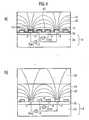
- FIG. 4a is the structure of the carrier 14 from the actual usually single-crystalline chip carrier, so the substrate 34, for example, silicon, and an electrically insulating layer 36, for example, silicon oxide, shown.
- the electrodes 2, 4, 8 and 10 are electrically insulated from each other.
- the analyte 38 which is in contact with the chip surface and the electrodes, is penetrated by current lines 40 which terminate in the polarization electrodes 2 and 4.
- These current lines 40 are formed by the feeding of the polarization current from the current source 6 by means of the polarization electrodes 2 and 4 in the analytes 38.
- catcher molecules can be mounted in a very thin layer 42 directly on the chip surface. Methods for this are well known from the prior art.
- a target molecule from the analyte 38 may diffuse to the capture molecule in the layer 42. Only in layer 42 can binding events take place at all and only be detected there. The detection takes place because in layer 42 the electrical properties of the medium change due to the bonding events.
- the current and voltage conditions in the analyte 38 change and at the sensor electrodes 8 and 10, a correspondingly changed voltage is tapped. As can be seen from the course of the streamlines 40, however, only a very small proportion of the field-interspersed space is used for the reaction.
- the changes in the electrical properties of the analyte which occur in such an arrangement and thus the detectable voltages between the sensor electrodes 8 and 10 may optionally be below the metrologically detectable range of measuring voltages.
- reaction layer 44 for example a hydrogel
- catcher molecules can be embedded or fixed in their entire volume.
- the reaction layer 44 is only about 5-10 microns thick.
- the chemical reaction or change of electrical parameters in the reaction layer 44 is thus penetrated by a substantially larger range of streamlines 40. In a reaction, therefore, much larger voltages are measured at the voltmeter 12.
- FIGS. 5a and 5b lie the polarizing electrodes 2 and 4 on electrically insulating webs 46 spaced from the surface of the carrier 14. This may result in certain cases, that is, for certain combinations of immobilized species and analyte, to a more favorable field distribution in the analyte 48.
- Cheaper means that between the sensor electrodes 8 and 10 as large a voltage difference across the voltmeter 12 can be measured.
- FIG. 5a the two sensor electrodes 8 and 10 are partially buried in the carrier 14.
- FIG. 5b These two electrodes are completely buried and thus galvanically separated from the analyte space 48.
- the degree of burial or galvanic separation may be more favorable or less favorable for achieving reliable readings on the voltmeter 12 depending on the analyte 38 and immobilized species.
- the choice of webs 46 as a support for the polarization electrodes 2 and 4 may be cheaper or less favorable depending on the case. A corresponding selection of the structural arrangement can be found experimentally in most cases.
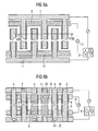
- FIGS. 6a and 6b show again different embodiments for the design or the connection technology of the various electrodes with respect to the layout and the technologies used in the semiconductor process in chip manufacture.
- Fig. 6a with respect to the polarizing electrodes 2 and 4 of the embodiment in FIG Fig. 1 ,
- the sensor electrodes 8 and 10 in about the same layout as the polarization electrodes 2 and 4, but below, separated by an electrically insulating intermediate layer, ie webs 46.
- a section through this arrangement is in Fig. 8 shown.
- Such a construction of the DNA chip achieves a very compact construction, which permits almost the smallest possible structure size and distances to one another for both electrode types, that is to say sensor and polarization electrodes 4 and 2, in the semiconductor process.
- the effective ratio between the sizes of both electrode types becomes similar to that in FIG Fig. 3
- the sensor electrodes 8 and 10 show a small size in relation to the polarization electrodes 2 and 4.
- Fig. 6b corresponds to the in Fig. 2 arrangement shown, except that here too, as in Fig. 6a that electrode types are stacked on top of each other rather than side by side.
- the polarization electrodes 2 and 4 are again on the electrically insulating webs 46 on the sensor electrodes 10 and 8, wherein the webs are not apparent from the plan view.
- a section along the line AA through the arrangement as in Fig. 6a corresponds here too FIG. 8 , Only that the superimposed electrodes are reversed, so the polarizing electrodes 2 and 4 are above the sensor electrodes 10 and 8 respectively.
- each sensor electrode 8 and 10 are associated with two shielding electrodes 50 and 52, respectively.
- buffer amplifier 54 the respective electrical potential of the sensor electrodes 8 and 10 is kept electrically active on the shield electrodes 50 and 52.
- the parasitic capacitances 56, 58 and 60 between sensor electrodes 8 and 10 and polarization electrodes 2 and 4 which are effective in the case of missing shielding electrodes, become partially electrically ineffective as a result of this measure, as is readily apparent from an electrical equivalent circuit diagram (not shown) of the arrangement.
- existing shielding electrodes namely, the parasitic capacitances 62 to 74 are formed.
- the capacitances 62, 68 and 74 are effective for the measurement in the measuring devices voltmeter 12 and the current meter associated with the current source 6.
- the other capacitors are supplied via the buffer amplifiers 54, that is to say they are charged or discharged via these and thus are not included in the measurement, which i. A. leads to a significantly improved measurement result.
- these parasitic capacitances can no longer adversely affect the impedance between the sensor and polarization electrodes.
- the buffer amplifiers 54 can be realized directly in the carrier 14 below the electrode arrangement with the aid of semiconductor technology. As a result, signal paths are shortened, additional capacities kept as small as possible, and thus the frequency characteristics of the entire measuring arrangement are favorably influenced.
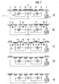
- FIG. 7 shown Embodiments of the arrangement of the individual electrodes differ in that one or more electrodes are galvanically isolated from the analyte or are completely or partially buried in the substrate. The galvanic isolation takes place as in Fig. 7a eg by oxidation of an additional oxide layer over the electrodes or by burying the electrodes, as in Fig. 7e performed for all electrodes involved. Also in Fig. 7 Again, various combinations between the alternatives presented are conceivable. These can be adapted to the needs of a specific measurement or design of the chip by simulations or in experiments.
- FIG. 8 various combinations of the arrangement of sensor and polarization electrodes are shown. While the polarization electrodes always rest on bars over the carrier, the sensor electrodes are arranged below or inside the bars.
- FIG. 9 shows configurations of electrodes according to the FIGS. 8 in which case additionally one or more shielding electrodes are provided between sensor electrodes with one another or between sensor and polarization electrodes. Also for the in FIG. 9 As far as the selection of a specific configuration is concerned, the statements made above apply to what has been said above.
Description
Die Erfindung betrifft einen DNA-Chip mit einem Mikroarray aus Mikroelektrodensystemen entsprechend dem Patentanspruch 1.The invention relates to a DNA chip with a microarray of microelectrode systems according to claim 1.
Ein DNA-Chip umfasst allgemein einen meist flach ausgebildeten Träger, auf dem ein Mikroarray aus Spots angeordnet ist. Ein Spot enthält auf den Oberflächen von Träger und Elektroden immobilisierte Fängermoleküle, beispielsweise Oligonucleotide. Zur Durchführung einer Analyse wird auf die Spots eine Zielmoleküle, beispielsweise DNA-Bruchstücke, enthaltende Analytlösung aufgebracht. Im Falle einer komplementären Übereinstimmung in der Basensequenz koppeln die Zielmoleküle an die Fängermoleküle eines Spots an. Die Auslesung des Analysenergebnisses, also die Bestimmung jener Spots, in denen Kopplungs- bzw. Bindungsereignisse stattgefunden haben, kann beispielsweise optisch, kalorimetrisch oder elektrisch erfolgen.A DNA chip generally comprises a generally flat carrier on which a microarray of spots is arranged. A spot contains capture molecules immobilized on the surfaces of supports and electrodes, for example oligonucleotides. To carry out an analysis, a target molecule, for example DNA fragments, containing analyte solution is applied to the spots. In the case of a complementary match in the base sequence, the target molecules couple to the capture molecules of a spot. The reading of the result of the analysis, ie the determination of those spots in which coupling or binding events have taken place, can take place, for example, optically, calorimetrically or electrically.
Aus der
Problematisch bei derartigen DNA-Chips ist, dass die Dimension der Elektroden sehr groß ist im Vergleich zu den molekularen Dimensionen der in monomolekularer Lage auf der Träger- und Elektrodenoberfläche vorhandenen Fängermoleküle. Dort stattfindende Bindungsereignisse sind daher nur schwer detektierbar. Bei van Gerwen et al wird zur Verbesserung des Messeffektes bzw. der Sensitivität eine Verkleinerung der Elektroden vorgeschlagen. Einer Miniaturisierung sind jedoch aus technischen und ökonomischen Gründen Grenzen gesetzt.The problem with such DNA chips is that the dimension of the electrodes is very large in comparison to the molecular ones Dimensions of capture molecules present in monomolecular position on the support and electrode surfaces. There binding events are therefore difficult to detect. In van Gerwen et al., A reduction of the electrodes is proposed to improve the measuring effect or the sensitivity. However, miniaturization is limited for technical and economic reasons.
Ein weiteres Problem besteht darin, dass beim Nachweis von biochemischen Molekülen relativ hohe Elektrolytleitwerte und dementsprechend niedrige Analytwiderstände vorliegen. Diese werden von der meist sehr hohen, durch die Elektrolyt-Doppelschichtkapazität zwischen Elektroden und Analyt hervorgerufene, Elektrodenimpedanz überlagert. Eine Separierung von Analytwiderstand und Elektrodenimpedanz ist nahezu unmöglich. Außerdem sind aufgrund des kleinen Analytwiderstandes sehr hohe Messfrequenzen nötig. Dies ist mit herkömmlicher Messtechnik jedoch sehr schwierig, da parasitäre Kapazitäten, wie Kabelkapazitäten etc., die Messung stören.Another problem is that the detection of biochemical molecules relatively high electrolyte conductance and accordingly low analyte resistances are present. These are superimposed by the usually very high electrode impedance caused by the electrolyte double layer capacitance between electrodes and analyte. Separation of analyte resistance and electrode impedance is nearly impossible. In addition, very high measurement frequencies are necessary due to the small analyte resistance. However, this is very difficult with conventional measuring technology, since parasitic capacitances, such as cable capacitances etc., disturb the measurement.
Bei herkömmlichen DNA-Chips sind also die Messeffekte zur Ermittlung der Kapazität bzw. des Widerstands des Analyten sehr schwach ausgeprägt oder nicht vorhanden. Darüber hinaus müssen die Messfrequenzen im MHz-Bereich liegen. Außerdem beeinflussen alle chemischen oder physikalischen Vorgänge, die an den Elektroden stattfinden, die Messung zwischen den Elektroden, so z.B. Belegungen mit biochemischen Molekülen, Polarisierungen, Korrosion der Elektroden, Filmbildung usw.In the case of conventional DNA chips, therefore, the measurement effects for determining the capacitance or the resistance of the analyte are very weak or absent. In addition, the measurement frequencies must be in the MHz range. In addition, any chemical or physical processes taking place on the electrodes affect the measurement between the electrodes, e.g. Assignment with biochemical molecules, polarization, electrode corrosion, film formation, etc.
Weiterhin ist aus
Das Dokument
Ausgehend vom Stand der Technik ist es Aufgabe der Erfindung, einen verbesserten elektrisch auslesbaren DNA-Chip zu schaffen, mit dem die Erfassung von analytspezifischen Messwerten erleichtert ist.Starting from the prior art, it is an object of the invention to provide an improved electrically readable DNA chip, with which the detection of analyte-specific measured values is facilitated.
Diese Aufgabe wird durch die Gesamtheit der Merkmale des Patentanspruches 1 gelöst. Weiterbildungen sind in den Unteransprüchen angegeben.This object is solved by the entirety of the features of claim 1. Further developments are specified in the subclaims.
Bei der Erfindung ist das Mikroelektrodensystem als Dünneschicht-Vierpolsystem aufgebaut. Dabei umfasst der DNA-Chip ein Paar Polarisationselektroden zur Erzeugung eines elektromagnetischen Wechselfeldes und ein Paar Sensorelektroden zur Messung eines bindungsinduzierten Spannungsabfalls im Analyten. Die Polarisationselektroden sind dabei mit Wechselstrom bzw. -spannung gegebener Amplitude und gegebener Frequenz beaufschlagt. Mit Hilfe der Sensorelektroden und eines an sie angeschlossenen hochohmigen Messverstärkers lässt sich eine durch Bindungsereignisse hervorgerufene Widerstandänderung als Spannungsänderung polarisierungsfrei abgreifen. Der störende Einfluss der Elektrodenimpedanz ist somit eliminiert. Der Spannungsabgriff an den Sensorelektroden erfolgt hochohmig, so dass keine nennenswerten Ströme aus den Sensorelektroden aus- oder in diese eintreten. Auch findet hierdurch an den Sensorelektroden keine zusätzliche Polarisation statt, was die oben beschriebenen nachteiligen Effekte wie Polarisation, Filmbildung, Oxidation etc. minimiert. Diese Effekte können zwar nach wie vor an den Polarisationselektroden auftreten, gehen jedoch wegen der Spannungsmessung rein über die Sensorelektroden nicht oder nur wesentlich geringer in die Messergebnisse ein.In the invention, the microelectrode system is constructed as a thin-film quadrupole system. In this case, the DNA chip comprises a pair of polarization electrodes for generating an alternating electromagnetic field and a pair of sensor electrodes for measuring a binding-induced voltage drop in the analyte. The polarization electrodes are supplied with alternating current or voltage of given amplitude and given frequency. With the aid of the sensor electrodes and a high-impedance measuring amplifier connected to them, a resistance change caused by binding events can be tapped without polarization as a voltage change. The disturbing influence of the electrode impedance is thus eliminated. The voltage tap on the sensor electrodes is high-impedance, so that no significant currents from the sensor electrodes or enter this. As a result, no additional polarization takes place at the sensor electrodes, which minimizes the adverse effects described above, such as polarization, film formation, oxidation, etc. Although these effects can still occur at the polarization electrodes, they do not go into the measurement results, or only considerably less because of the voltage measurement purely via the sensor electrodes.
Durch die Trennung von polarisierenden Polarisationselektroden und messenden Sensorelektroden, an denen praktisch keine störenden chemischen oder physikalischen Vorgänge stattfinden, wird vorteilhafterweise die Qualität der Messung erheblich gesteigert. Dabei ist der Aufbau des Vierpolsystems mit Dünnschichtelektroden wesentlich, wobei solche Dünnschichtelektroden vorteilhafterweise durch die in der Halbleitertechnologie bekannten Verfahren in den Chip integriert werden können.By separating polarizing polarizing electrodes and measuring sensor electrodes, in which virtually no interfering chemical or physical processes take place, the quality of the measurement is advantageously increased considerably. Here is the structure of the quadrupole system with Thin-film electrodes substantially, wherein such thin-film electrodes can be advantageously integrated into the chip by the methods known in semiconductor technology.
Bei einer bevorzugten Ausgestaltung der Erfindung weist der Träger des DNA-Chips ein Siliziumsubstrat auf, auf dem das Mikroelektrodensystem vorzugsweise in Dünnfilmtechnik integriert ist. Dabei sind die Elektroden direkt an eine sich im Si-Substrat befindliche integrierte Schaltung angeschlossen. Vorteilhaft dabei ist insbesondere das Fehlen von Zuleitungskapazitäten, welche sich vor allem bei Messungen im höheren Frequenzbereich, z.B. ab 10 MHz störend bemerkbar machen würden. Ein DNA-Chip der genannten Ausgestaltung ist somit auch bei hohen Messfrequenzen anwendbar.In a preferred embodiment of the invention, the carrier of the DNA chip has a silicon substrate on which the microelectrode system is preferably integrated in thin-film technology. In this case, the electrodes are connected directly to an integrated circuit located in the Si substrate. Particularly advantageous here is the lack of supply capacitances, which are particularly important for measurements in the higher frequency range, e.g. from 10 MHz would make disturbing noticeable. A DNA chip of the stated embodiment is therefore also applicable at high measurement frequencies.
Trotz der beschriebenen Maßnahmen sind noch weitere Parasitärkapazitäten zwischen den an der Messung beteiligten Elektroden vorhanden, die in ungünstigen Fällen störend bei der Impedanzmessung im Analyten sein können. Um hier Abhilfe zu schaffen, ist bei der Erfindung einer Sensorelektrode eine Schirmelektrode zugeordnet, die auf dem gleichen elektrischen Potential wie die Sensorelektrode gehalten ist. Vorzugsweise wird das elektrische Potential der Sensorelektrode an der Schirmelektrode durch einen an der Sensorelektrode angeschlossenen Pufferverstärker mit Verstärkung 1 gehalten. Der Pufferverstärker als aktives elektronisches Element entkoppelt Potential und Stromstärke, bzw. Ladung. Die zwischen den zusätzlichen Schirmelektroden und den anderen Elektroden auftretenden Parasitärkapazitäten sind so für die Messung elektrisch nicht wirksam, da das Laden oder Entladen der Kapazitäten vom aktiven Verstärker übernommen wird und so das Messgerät und die Sensorelektroden zur Potentialmessung entlastet sind. Schirmelektroden können z.B. beidseits der Sensorelektroden ausgeführt sein oder nur zwischen Sensorelektroden und Polarisationselektroden liegen. Die Effekte der Abschirmung durch die Schirmelektroden und die anwachsende Distanz einer Elektrodeneinheit durch Einfügen von Schirmelektroden sind im Einzelfall gegeneinander abzuwägen.Despite the measures described, further parasitic capacitances are present between the electrodes involved in the measurement, which in unfavorable cases can be disturbing in the impedance measurement in the analyte. To remedy this situation, in the invention of a sensor electrode, a shield electrode is associated, which is held at the same electrical potential as the sensor electrode. Preferably, the electric potential of the sensor electrode is held on the shield electrode by a gain-1 buffer amplifier connected to the sensor electrode. The buffer amplifier as an active electronic element decouples potential and current, or charge. The parasitic capacitances occurring between the additional shielding electrodes and the other electrodes are thus not electrically effective for the measurement, since the charging or discharging of the capacitances is taken over by the active amplifier, thus relieving the measuring device and the sensor electrodes for potential measurement. Shield electrodes can be designed, for example, on both sides of the sensor electrodes or lie only between sensor electrodes and polarization electrodes. The effects of shielding by the Screen electrodes and the increasing distance of an electrode unit by inserting shielding electrodes are to be weighed against each other in individual cases.
Der Pufferverstärker ist auf dem DNA-Chip integriert. Hierdurch ergibt sich ein besonders kompakter und wirkungsvoller Aufbau des DNA-Chips. Die Zuleitungen werden so kurz wie möglich gehalten und damit Störungen in sämtlichen Signalleitungen so gut wie möglich ausgeschlossen.The buffer amplifier is integrated on the DNA chip. This results in a particularly compact and effective structure of the DNA chip. The supply lines are kept as short as possible, thus eliminating interference in all signal lines as much as possible.
Um einen die Messung verfälschenden Stromfluss innerhalb der Sensorelektroden und auch der Schirmelektroden zu vermeiden, sollten diese Elektroden deutlich kleiner sein als die Potentialelektroden. Bei einer Breite der Potentialelektroden von 1 µm würde dies für die genannten Elektroden eine technisch nicht mehr realisierbare weitere Verkleinerung bedeuten. Bei einer bevorzugten Ausführungsform wird daher ein anderer Weg beschritten. Hier sind Sensor- und/oder Schirmelektroden gänzlich galvanisch vom Analyten getrennt und damit ein Stromfluss zwischen Analyt und Elektroden verhindert.In order to avoid a flow of current which falsifies the measurement within the sensor electrodes and also the shield electrodes, these electrodes should be significantly smaller than the potential electrodes. Given a width of the potential electrodes of 1 μm, this would mean a further reduction that would no longer be technically feasible for the electrodes mentioned. In a preferred embodiment, therefore, another approach is taken. Here sensor and / or shield electrodes are completely galvanically separated from the analyte and thus prevents a flow of current between analyte and electrodes.
Bei einem anderen bevorzugten Ausführungsbeispiel wird dies durch eine punktförmige Ausgestaltung der Sensorelektroden erreicht. Dabei ist es erforderlich, dass eine Einrichtung zum Abgriff des Spannungsabfalls an den Sensorelektroden einen hohen Eingangswiderstand und eine niedrige Eingangskapazität aufweist. Die elektrische Verbindung der punktförmigen Sensorelektroden wird vorzugsweise durch eine im Substrat eingebettete ("vergrabene") Sammelleitung bewerkstelligt, die über Durchkontaktierungen mit den Sensorelektroden elektrisch verbunden ist.In another preferred embodiment, this is achieved by a punctiform configuration of the sensor electrodes. In this case, it is necessary that a device for picking up the voltage drop across the sensor electrodes have a high input resistance and a low input capacitance. The electrical connection of the point-shaped sensor electrodes is preferably accomplished by a ("buried") busbar embedded in the substrate, which is electrically connected via plated-through holes to the sensor electrodes.
Um die Tauglichkeit eines DNA-Chips als biochemisches Analysesystem zu gewährleisten, müssen die Elektrodengeometrien und damit der impedanzspektroskopische Erfassungsbereich möglichst an die Dimensionen biochemischer Moleküle angenähert werden. Eine Elektrodenbreiten von etwa 500 nm unterschreitende Miniaturisierung ist jedoch nur mit aufwendigster Technik zu sehr hohen Kosten realisierbar. Dabei kommt bei einem 4-Elektrodensystem erschwerend hinzu, dass der Abstand der Polarisationselektroden zueinander von Haus aus größer ist als bei einem 2-Elektrodensystem, weil ja zwischen den Polarisationselektroden weitere, z.B. die Sensorelektroden liegen. Bei einer besonders bevorzugten Ausführungsvariante ist nun eine das Mikroelektrodensystem einbettende Reaktionsschicht vorgesehen, welche den Raum, in dem Bindungsereignisse stattfinden und impedanzspektroskopisch erfasst werden können, wesentlich vergrößert. Mit der Reaktionsschicht lässt sich somit die Anzahl von erfassbaren Bindungsereignissen und damit der Messeffekt bzw. die Sensitivität eines DNA-Chips erheblich steigern.In order to ensure the suitability of a DNA chip as a biochemical analysis system, the electrode geometries and thus the impedance spectroscopic detection range must be approximated as far as possible to the dimensions of biochemical molecules. An electrode width of about 500 nm below However, miniaturization can only be achieved at very high costs with the most sophisticated technology. In this case, in a 4-electrode system, the distance of the polarization electrodes from one another is inherently greater than in the case of a 2-electrode system, because there are additional electrodes, for example the sensor electrodes, between the polarization electrodes. In a particularly preferred embodiment variant, a reaction layer embedding the microelectrode system is now provided which substantially increases the space in which binding events take place and can be detected by impedance spectroscopy. With the reaction layer, the number of detectable binding events and thus the measurement effect or the sensitivity of a DNA chip can be significantly increased.
Die Reaktionsschicht hat vorzugsweise eine Dicke, die mit der Breite der Elektroden korreliert ist, und entspricht vorteilhafterweise etwa dem 5-10fachen der Elektrodenbreite. In jedem Fall sollte die Reaktionsschicht eine Dicke unter 100 µm, da sich sonst zu lange Diffusionswege und damit verbunden zu lange Reaktionszeiten für den Transport der Zielmoleküle zu den Fängermolekülen ergeben würden. Geht man von 1 µm (1000 nm) als Elektrodenbreite aus, liegt die Dicke der Reaktionsschicht etwa 5 bis 10 µm. Damit ist gewährleistet, dass die in einer auf die Reaktionsschicht aufgebrachten Analytlösung enthaltenen Zielmoleküle mit ausreichender Geschwindigkeit eindiffundieren können. Als besonders geeignet haben sich Hydrogele zum Aufbau einer Reaktionsschicht herausgestellt.The reaction layer preferably has a thickness which is correlated with the width of the electrodes, and advantageously corresponds to about 5-10 times the electrode width. In any case, the reaction layer should have a thickness of less than 100 μm, since otherwise too long diffusion paths and, associated therewith, too long reaction times would result for the transport of the target molecules to the capture molecules. Assuming 1 μm (1000 nm) as the electrode width, the thickness of the reaction layer is about 5 to 10 μm. This ensures that the target molecules contained in an analyte solution applied to the reaction layer can diffuse at a sufficient rate. Hydrogels have proven particularly suitable for the construction of a reaction layer.
Weitere Einzelheiten und Vorteile der Erfindung ergeben sich aus der nachfolgenden Figurenbeschreibung von Ausführungsbeispielen anhand der Zeichnung in Verbindung mit den Patentansprüchen. Es zeigen
- Fig. 1
- die Draufsicht auf einen DNA-Chip mit Elektrodenmikrosystem in Interdigitalstruktur,
- Fig. 2
- die Draufsicht auf ein Elektrodenmikrosystem mit vergrabenen Sammelleitungen,
- Fig. 3
- die Draufsicht auf ein Elektrodenmikrosystem mit punktförmigen Sensorelektroden,
- Fig. 4
- den Schnitt durch das Elektrodenmikrosystem aus
Fig. 1 entlang der Linie IV-IV ohne (a) und mit (b) einer Reaktionsschicht, - Fig. 5
- den Schnitt durch das Elektrodenmikrosystem aus
Fig. 1 entlang der Linie IV-IV mit auf Stegen liegenden und teilweise (a) bzw. ganz (b) vergrabenen Elektroden, - Fig. 6
- Elektrodenanordnungen in Draufsicht in Interdigitalstruktur (a) bzw. mit vergrabenen Elektrodensammelleitungen und Durchkontaktierungen (b),
- Fig. 7
- Elektrodenanordnungen im Querschnitt mit Schirmelektroden und verschieden isolierten bzw. vergrabenen Elektroden (a) bis (e),
- Fig. 8
- Elektrodenanordnungen im Querschnitt mit übereinander liegenden Polarisations- und Sensorelektroden in verschiedenen Ausführungsformen (a) bis (f),
- Fig. 9
- Elektrodenanordnungen im Querschnitt mit Beispielen von Kombinationen der unterschiedlichen Anordnungstechniken (a) bis (d), jeweils in Prinzipdarstellung.
- Fig. 1
- the top view of a DNA chip with electrode microsystem in interdigital structure,
- Fig. 2
- the top view of an electrode microsystem with buried manifolds,
- Fig. 3
- the top view of an electrode microsystem with punctiform sensor electrodes,
- Fig. 4
- the cut through the electrode microsystem
Fig. 1 along the line IV-IV without (a) and with (b) a reaction layer, - Fig. 5
- the cut through the electrode microsystem
Fig. 1 along the line IV-IV with lying on webs and partially (a) or completely (b) buried electrodes, - Fig. 6
- Electrode arrangements in plan view in interdigital structure (a) or with buried electrode busbars and plated-through holes (b),
- Fig. 7
- Electrode arrangements in cross-section with shielding electrodes and differently isolated or buried electrodes (a) to (e),
- Fig. 8
- Electrode arrangements in cross-section with superimposed polarization and sensor electrodes in various embodiments (a) to (f),
- Fig. 9
- Electrode arrangements in cross section with examples of combinations of the different arrangement techniques (a) to (d), respectively in schematic representation.
Weiterhin ist in
In
Die in
Zur elektrischen Verbindung ist hier jedem Elektrodentyp eine Elektrodensammelleitung zugeordnet. Der Polarisationselektrode 2 ist zum Beispiel die Sammelleitung 18 zugeordnet. Die beiden Streifen der Polarisationselektrode 2 sind deshalb mit Hilfe von elektrischen Durchkontaktierungen 20 mit der ihr zugeordneten Sammelleitung 18 verbunden. Gegenüber allen anderen Elektroden 4, 8 und 10 ist die Sammelleitung 18 elektrisch isoliert. Deshalb liegen Sammelleitungen zum Beispiel vergraben in der Isolierenden Deckschicht 36 des Trägers 14 oder sind zumindest sowohl gegeneinander als auch gegenüber allen Elektroden anderweitig elektrisch isoliert. Der zweiten Polarisationselektrode 4 ist die Sammelleitung 22 mit entsprechenden Durchkontaktierungen 24 zugeordnet usw.For electrical connection here each electrode type is assigned an electrode manifold. The
In
Jede Einzelelektrode 28 enthält einen punktförmigen Elektrodenkopf 30, der mit Hilfe einer elektrischen Durchkontaktierung 32 mit der Elektrodensammelleitung 26 verbunden ist. Obwohl die Elektrodenbreite w und der Elektrodenabstand g gleich sind, wird durch diese Maßnahme erreicht, dass die effektive Elektrodenfläche der Sensorelektroden 8 und 10 gegenüber der Fläche der Polarisationselektroden 2 und 4 wesentlich kleiner ist. Hier ist nochmals angedeutet, dass in realen Anordnungen die "Länge" 1 der Elektrode wesentlich größer als deren Breite w ist.Each
Ein Schnitt durch die
Bei letzterer Anordnung können Fängermoleküle in einer sehr dünnen Schicht 42 direkt auf der Chipoberfläche angebracht werden. Methoden hierzu sind aus dem Stand der Technik hinreichend bekannt. Ein Zielmolekül aus dem Analyten 38 kann zum Fängermolekül in der Schicht 42 diffundieren. Nur in der Schicht 42 können so Bindungsereignisse überhaupt stattfinden und nur dort detektiert werden. Die Detektion findet statt, weil in der Schicht 42 sich die elektrischen Eigenschaften des Mediums aufgrund der Bindungsereignisse ändern. Die Strom- und Spannungsverhältnisse im Analyten 38 ändern sich und an den Sensorelektroden 8 und 10 wird eine entsprechend geänderte Spannung abgegriffen. Wie aus dem Verlauf der Stromlinien 40 ersichtlich, wird jedoch nur ein sehr geringer Anteil des felddurchsetzten Raumes zur Reaktion benutzt. Die in einer derartigen Anordnung auftretenden Veränderungen der elektrischen Eigenschaften des Analyten und somit die detektierbaren Spannungen zwischen den Sensorelektroden 8 und 10 können gegebenenfalls unterhalb des messtechnisch erfassbaren Bereiches von Messspannungen liegen.In the latter arrangement catcher molecules can be mounted in a very
Eine Verbesserung kann durch das Aufbringen einer Reaktionsschicht 44 auf den DNA-Chip stattfinden, wie in
In den
In
Die
Die Auswahl der verwendeten Technologien bzw. Layouts richtet sich meist nach den Gegebenheiten bzw. Randbedingungen des zu verwendenden Halbleiterprozesses und der mit dem DNA-Chip zu lösenden Aufgabe. Natürlich können auch Kombinationsmöglichkeiten aus den vorgestellten Techniken verwendet werden. So ist es zum Beispiel denkbar, die Polarisationselektroden gemäß
In der
Die Pufferverstärker 54 können mit_Hilfe der Halbleitertechnologie direkt im Träger 14 unterhalb der Elektrodenanordnung realisiert werden. Hierdurch werden Signalwege verkürzt, zusätzliche Kapazitäten so klein wie möglich gehalten, und somit die Frequenzeigenschaften der gesamten Messanordnung günstig beeinflusst. Die verschiedenen in
Auch in
Die in den Figuren dargestellten Ausführungsformen sind Beispiele für die verschiedenen Kombinationsmöglichkeiten aus den aufgeführten Techniken. Natürlich sind, wie mehrfach erwähnt auch andere als die explizit dargestellten Kombinationen möglich.The embodiments shown in the figures are examples of the various possible combinations of the listed techniques. Of course, as mentioned above, combinations other than those explicitly shown are possible.
Claims (11)
- DNA chip comprising a carrier (14) and, arranged thereon, a microarray of spots (1) containing immobilized catcher molecules, each spot (1) containing a microelectrode system for the impedance-spectroscopic detection of binding events between the catcher molecules and target molecules of an analyte solution (38) applied to the spots (1), the microelectrode system being a thin-film four-pole system, and the thin-film four-pole system comprising two polarization electrodes (2, 4) for generating an alternating electromagnetic field and two sensor electrodes (8, 10) for measuring a voltage drop in the analyte (38), and at least one sensor electrode (8, 10) being assigned a shielding electrode (50, 52), which is held at the same electrical potential as the sensor electrode (8, 10).
- DNA chip according to Claim 1, characterized in that the carrier (14) comprises a silicon substrate (34), on which the microelectrode system is integrated using thin-film technology.
- DNA chip according to either of Claims 1 and 2, characterized in that the electrical potential of the sensor electrode (8, 10) is held at the shielding electrode (50, 52) by a buffer amplifier (54) connected to the sensor electrode (8, 10) and having a gain of 1.
- DNA chip according to Claim 3, characterized in that the buffer amplifier (54) is integrated on the carrier (14).
- DNA chip according to one of the preceding claims, characterized in that at least one sensor electrode (8, 10) and/or at least one shielding electrode (50, 52) are directly electrically isolated from the analyte (38).
- DNA chip according to one of the preceding claims, characterized in that a sensor electrode (8, 10) contains pointlike individual electrodes (28) which are electrically connected to a buried electrode collective line (26) by means of plated-through holes (32).
- DNA chip according to one of the preceding claims, characterized in that the thin-film microelectrode system is embedded in a reaction layer (44) containing catcher molecules.
- DNA chip according to Claim 7, characterized in that the thickness of the reaction layer (44) is less than 100 µm and is correlated with the width of the electrodes or the interspaces thereof.
- DNA chip according to Claim 8, the width of the electrodes being approximately 1 µm, characterized in that the thickness of the reaction layer (44) corresponds to approximately 5-10 times the value of the electrode width.
- DNA chip according to Claim 7 or 8, characterized in that the reaction layer (44) is a hydrogel.
- DNA chip according to one of the preceding claims, characterized in that the thin-film four-pole system forms an interdigital current electrode arrangement with double meandering current taps.
Applications Claiming Priority (3)
| Application Number | Priority Date | Filing Date | Title |
|---|---|---|---|
| DE10259820A DE10259820B4 (en) | 2002-12-19 | 2002-12-19 | DNA chip |
| DE10259820 | 2002-12-19 | ||
| PCT/DE2003/004127 WO2004057334A1 (en) | 2002-12-19 | 2003-12-15 | Dna chip comprising a microarray made of an microelectrode system |
Publications (2)
| Publication Number | Publication Date |
|---|---|
| EP1573327A1 EP1573327A1 (en) | 2005-09-14 |
| EP1573327B1 true EP1573327B1 (en) | 2013-10-16 |
Family
ID=32404018
Family Applications (1)
| Application Number | Title | Priority Date | Filing Date |
|---|---|---|---|
| EP03795750.3A Expired - Lifetime EP1573327B1 (en) | 2002-12-19 | 2003-12-15 | Dna chip comprising a microarray made of microelectrode systems |
Country Status (7)
| Country | Link |
|---|---|
| US (1) | US7572624B2 (en) |
| EP (1) | EP1573327B1 (en) |
| JP (1) | JP4287819B2 (en) |
| CA (1) | CA2510720C (en) |
| DE (1) | DE10259820B4 (en) |
| DK (1) | DK1573327T3 (en) |
| WO (1) | WO2004057334A1 (en) |
Families Citing this family (14)
| Publication number | Priority date | Publication date | Assignee | Title |
|---|---|---|---|---|
| DE102004045210A1 (en) | 2004-09-17 | 2006-04-06 | Infineon Technologies Ag | Sensor arrangement and method for determining a sensor event |
| JP4615962B2 (en) * | 2004-10-22 | 2011-01-19 | ルネサスエレクトロニクス株式会社 | Semiconductor device |
| KR100969671B1 (en) * | 2008-03-28 | 2010-07-14 | 디지탈 지노믹스(주) | High sensitive biosensor, biochip comprising the same and manufacturing method therefor |
| WO2009132667A1 (en) * | 2008-04-30 | 2009-11-05 | Micronas Gmbh | Method for verifying and/or determining the concentration of a ligand |
| US9678055B2 (en) | 2010-02-08 | 2017-06-13 | Genia Technologies, Inc. | Methods for forming a nanopore in a lipid bilayer |
| US9605307B2 (en) | 2010-02-08 | 2017-03-28 | Genia Technologies, Inc. | Systems and methods for forming a nanopore in a lipid bilayer |
| JP5786295B2 (en) * | 2010-06-22 | 2015-09-30 | ソニー株式会社 | Nucleic acid isothermal amplification microchip, method for producing the same, and nucleic acid isothermal amplification method |
| US8962242B2 (en) | 2011-01-24 | 2015-02-24 | Genia Technologies, Inc. | System for detecting electrical properties of a molecular complex |
| US9140658B1 (en) * | 2012-01-06 | 2015-09-22 | Enuresis Solutions Llc | Fluid detection device |
| US8986629B2 (en) | 2012-02-27 | 2015-03-24 | Genia Technologies, Inc. | Sensor circuit for controlling, detecting, and measuring a molecular complex |
| US9759711B2 (en) | 2013-02-05 | 2017-09-12 | Genia Technologies, Inc. | Nanopore arrays |
| US9983163B2 (en) | 2013-04-30 | 2018-05-29 | Board Of Regents, The University Of Texas System | Integrated electro-analytical biosensor array |
| US9551697B2 (en) | 2013-10-17 | 2017-01-24 | Genia Technologies, Inc. | Non-faradaic, capacitively coupled measurement in a nanopore cell array |
| CN106497774A (en) * | 2017-01-03 | 2017-03-15 | 京东方科技集团股份有限公司 | Gene sequencing chip, gene sequencing equipment and gene order surveying method |
Family Cites Families (20)
| Publication number | Priority date | Publication date | Assignee | Title |
|---|---|---|---|---|
| JPS55138397A (en) | 1979-04-13 | 1980-10-29 | Fujisawa Pharmaceut Co Ltd | Method of measurement of bacterium growth rate and device therefor |
| JP2504069B2 (en) | 1987-09-10 | 1996-06-05 | いすゞ自動車株式会社 | Control device for turbocharger with rotating electric machine |
| AT403528B (en) * | 1989-04-04 | 1998-03-25 | Urban Gerald | MICRO-MULTI-ELECTRODE STRUCTURE FOR ELECTROCHEMICAL APPLICATIONS AND METHOD FOR THEIR PRODUCTION |
| US5846708A (en) | 1991-11-19 | 1998-12-08 | Massachusetts Institiute Of Technology | Optical and electrical methods and apparatus for molecule detection |
| JP2590728B2 (en) | 1994-04-21 | 1997-03-12 | 日本電気株式会社 | Selective growth method of compound semiconductor |
| US5567301A (en) * | 1995-03-01 | 1996-10-22 | Illinois Institute Of Technology | Antibody covalently bound film immunobiosensor |
| DE19610115C2 (en) * | 1996-03-14 | 2000-11-23 | Fraunhofer Ges Forschung | Detection of molecules and molecular complexes |
| GB9622304D0 (en) * | 1996-10-26 | 1996-12-18 | Univ Manchester | Sensor |
| AU746549B2 (en) * | 1996-11-20 | 2002-05-02 | Becton Dickinson & Company | Microfabricated isothermal nucleic acid amplification devices and methods |
| US7087148B1 (en) * | 1998-06-23 | 2006-08-08 | Clinical Micro Sensors, Inc. | Binding acceleration techniques for the detection of analytes |
| US6485703B1 (en) * | 1998-07-31 | 2002-11-26 | The Texas A&M University System | Compositions and methods for analyte detection |
| US6169394B1 (en) * | 1998-09-18 | 2001-01-02 | University Of The Utah Research Foundation | Electrical detector for micro-analysis systems |
| DE19916921A1 (en) * | 1999-04-14 | 2000-10-19 | Fraunhofer Ges Forschung | Electrical sensor array |
| GB9908696D0 (en) * | 1999-04-17 | 1999-06-09 | Chandler Robert W | High impedance sensor apparatus and method for detecting fluids |
| US6303082B1 (en) | 1999-12-15 | 2001-10-16 | Nanogen, Inc. | Permeation layer attachment chemistry and method |
| DE10015816A1 (en) * | 2000-03-30 | 2001-10-18 | Infineon Technologies Ag | Biosensor chip |
| WO2001079828A1 (en) | 2000-04-14 | 2001-10-25 | Nanotec Solution | Device and method for determining characteristics of a biomass |
| US7435579B2 (en) * | 2000-04-17 | 2008-10-14 | Purdue Research Foundation | Biosensor and related method |
| CA2407973C (en) * | 2000-05-03 | 2011-06-07 | Jen-Jr Gau | Biological identification system with integrated sensor chip |
| DE10058397A1 (en) * | 2000-11-24 | 2002-06-06 | Siemens Ag | Arrangement for an electrochemical analysis method and its use |
-
2002
- 2002-12-19 DE DE10259820A patent/DE10259820B4/en not_active Expired - Lifetime
-
2003
- 2003-12-15 CA CA2510720A patent/CA2510720C/en not_active Expired - Lifetime
- 2003-12-15 DK DK03795750.3T patent/DK1573327T3/en active
- 2003-12-15 EP EP03795750.3A patent/EP1573327B1/en not_active Expired - Lifetime
- 2003-12-15 WO PCT/DE2003/004127 patent/WO2004057334A1/en active Application Filing
- 2003-12-15 JP JP2004561039A patent/JP4287819B2/en not_active Expired - Fee Related
- 2003-12-15 US US10/539,817 patent/US7572624B2/en not_active Expired - Lifetime
Also Published As
| Publication number | Publication date |
|---|---|
| JP2006510881A (en) | 2006-03-30 |
| CA2510720A1 (en) | 2004-07-08 |
| US7572624B2 (en) | 2009-08-11 |
| US20060216813A1 (en) | 2006-09-28 |
| WO2004057334A1 (en) | 2004-07-08 |
| EP1573327A1 (en) | 2005-09-14 |
| JP4287819B2 (en) | 2009-07-01 |
| DK1573327T3 (en) | 2013-12-16 |
| CA2510720C (en) | 2012-02-14 |
| DE10259820A1 (en) | 2004-07-01 |
| DE10259820B4 (en) | 2006-05-24 |
Similar Documents
| Publication | Publication Date | Title |
|---|---|---|
| EP1573327B1 (en) | Dna chip comprising a microarray made of microelectrode systems | |
| EP1516175B1 (en) | Biosensor array and method for operating a biosensor array | |
| EP1789811B1 (en) | Biosensor array and method for detecting a sensor event | |
| EP2707734B1 (en) | Contactless capacitive distance sensor | |
| DE10221084A1 (en) | Sensor arrangement for measuring a gas concentration | |
| DE10319664A1 (en) | Particle detection sensor | |
| DE10011562A1 (en) | Gas sensor | |
| DE102008050633A1 (en) | impedance sensor | |
| EP1761762B1 (en) | Planar-sensor arrangement, sensor array and method for the production of a planar-sensor arrangement | |
| EP1740935A1 (en) | Field effect transistor for measuring biocomponents | |
| DE10123920B4 (en) | Integrated microstructure sensor element for detecting thermodynamic quantities of a fluid | |
| EP1472548A2 (en) | Switching circuit system, electrochemical sensor, sensor system, and method for processing a current signal made available via a sensor electrode | |
| WO2005001479A1 (en) | Capacitative biosensor element and method for detecting hybridization events | |
| DE10014995C1 (en) | Electrochemical sensor for determining gas components or concentrations in gas mixtures comprises a sensor element having a signal-forming electrode with a feed surrounded by an electrically conducting screen | |
| DE102014210122A1 (en) | An apparatus for determining a value of a property of a fluid to be measured, a method for operating a device for determining a value of a property of a fluid to be measured, and a method for producing a device for determining a value of a property of a fluid to be measured | |
| EP1328799B1 (en) | Electronic circuit, sensor arrangement and method for processing a sensor signal | |
| DE10224567A1 (en) | Sensor arrangement and method for operating a sensor arrangement | |
| WO1993023758A1 (en) | Integratable conductivity measuring device | |
| DE10331299A1 (en) | Sensor-transistor element, sensor unit and sensor array | |
| EP1573328B1 (en) | Biochip | |
| DE10131581B4 (en) | Method and device for generating and checking composite arrangements | |
| EP3764054B1 (en) | Sensor arrangement for detecting a deflection of a wire electrode | |
| DE102021204556A1 (en) | Method and device for monitoring a measurement position with regard to the presence, quantity and/or type of a chemical occurring at the measurement position | |
| DE102022211374A1 (en) | Improved sensor arrangement based on a metal oxide sensor material structure | |
| WO2021123259A1 (en) | Sample carrier for electrical manipulation of liquid samples and for performing vibrational spectroscopy on the samples |
Legal Events
| Date | Code | Title | Description |
|---|---|---|---|
| PUAI | Public reference made under article 153(3) epc to a published international application that has entered the european phase |
Free format text: ORIGINAL CODE: 0009012 |
|
| 17P | Request for examination filed |
Effective date: 20050616 |
|
| AK | Designated contracting states |
Kind code of ref document: A1 Designated state(s): AT BE BG CH CY CZ DE DK EE ES FI FR GB GR HU IE IT LI LU MC NL PT RO SE SI SK TR |
|
| RAP1 | Party data changed (applicant data changed or rights of an application transferred) |
Owner name: SIEMENS AKTIENGESELLSCHAFT |
|
| RIN1 | Information on inventor provided before grant (corrected) |
Inventor name: SCHIENLE, MEINRAD Inventor name: MUND, KONRAD Inventor name: GUMBRECHT, WALTER Inventor name: THEWES, ROLAND |
|
| 17Q | First examination report despatched |
Effective date: 20101124 |
|
| RAP1 | Party data changed (applicant data changed or rights of an application transferred) |
Owner name: SIEMENS AKTIENGESELLSCHAFT |
|
| GRAP | Despatch of communication of intention to grant a patent |
Free format text: ORIGINAL CODE: EPIDOSNIGR1 |
|
| INTG | Intention to grant announced |
Effective date: 20130508 |
|
| GRAS | Grant fee paid |
Free format text: ORIGINAL CODE: EPIDOSNIGR3 |
|
| GRAA | (expected) grant |
Free format text: ORIGINAL CODE: 0009210 |
|
| AK | Designated contracting states |
Kind code of ref document: B1 Designated state(s): AT BE BG CH CY CZ DE DK EE ES FI FR GB GR HU IE IT LI LU MC NL PT RO SE SI SK TR |
|
| REG | Reference to a national code |
Ref country code: GB Ref legal event code: FG4D Free format text: NOT ENGLISH |
|
| REG | Reference to a national code |
Ref country code: CH Ref legal event code: EP Ref country code: CH Ref legal event code: NV Representative=s name: SIEMENS SCHWEIZ AG, CH |
|
| REG | Reference to a national code |
Ref country code: IE Ref legal event code: FG4D Free format text: LANGUAGE OF EP DOCUMENT: GERMAN |
|
| REG | Reference to a national code |
Ref country code: AT Ref legal event code: REF Ref document number: 636738 Country of ref document: AT Kind code of ref document: T Effective date: 20131115 |
|
| REG | Reference to a national code |
Ref country code: DE Ref legal event code: R096 Ref document number: 50314913 Country of ref document: DE Effective date: 20131205 |
|
| REG | Reference to a national code |
Ref country code: DK Ref legal event code: T3 Effective date: 20131210 |
|
| REG | Reference to a national code |
Ref country code: SE Ref legal event code: TRGR |
|
| REG | Reference to a national code |
Ref country code: NL Ref legal event code: T3 |
|
| PG25 | Lapsed in a contracting state [announced via postgrant information from national office to epo] |
Ref country code: FI Free format text: LAPSE BECAUSE OF FAILURE TO SUBMIT A TRANSLATION OF THE DESCRIPTION OR TO PAY THE FEE WITHIN THE PRESCRIBED TIME-LIMIT Effective date: 20131016 |
|
| RAP2 | Party data changed (patent owner data changed or rights of a patent transferred) |
Owner name: SIEMENS AKTIENGESELLSCHAFT |
|
| PG25 | Lapsed in a contracting state [announced via postgrant information from national office to epo] |
Ref country code: CY Free format text: LAPSE BECAUSE OF FAILURE TO SUBMIT A TRANSLATION OF THE DESCRIPTION OR TO PAY THE FEE WITHIN THE PRESCRIBED TIME-LIMIT Effective date: 20131016 Ref country code: ES Free format text: LAPSE BECAUSE OF FAILURE TO SUBMIT A TRANSLATION OF THE DESCRIPTION OR TO PAY THE FEE WITHIN THE PRESCRIBED TIME-LIMIT Effective date: 20131016 |
|
| PG25 | Lapsed in a contracting state [announced via postgrant information from national office to epo] |
Ref country code: PT Free format text: LAPSE BECAUSE OF FAILURE TO SUBMIT A TRANSLATION OF THE DESCRIPTION OR TO PAY THE FEE WITHIN THE PRESCRIBED TIME-LIMIT Effective date: 20140217 |
|
| REG | Reference to a national code |
Ref country code: DE Ref legal event code: R097 Ref document number: 50314913 Country of ref document: DE |
|
| REG | Reference to a national code |
Ref country code: DE Ref legal event code: R081 Ref document number: 50314913 Country of ref document: DE Owner name: BOEHRINGER INGELHEIM VETMEDICA GMBH, DE Free format text: FORMER OWNER: SIEMENS AKTIENGESELLSCHAFT, 80333 MUENCHEN, DE Effective date: 20140612 Ref country code: DE Ref legal event code: R081 Ref document number: 50314913 Country of ref document: DE Owner name: BOEHRINGER INGELHEIM VETMEDICA GMBH, DE Free format text: FORMER OWNER: SIEMENS AKTIENGESELLSCHAFT, INFINEON TECHNOLOGIES AG, , DE Effective date: 20131016 Ref country code: DE Ref legal event code: R081 Ref document number: 50314913 Country of ref document: DE Owner name: BOEHRINGER INGELHEIM VETMEDICA GMBH, DE Free format text: FORMER OWNERS: SIEMENS AKTIENGESELLSCHAFT, 80333 MUENCHEN, DE; INFINEON TECHNOLOGIES AG, 81669 MUENCHEN, DE Effective date: 20131016 |
|
| PG25 | Lapsed in a contracting state [announced via postgrant information from national office to epo] |
Ref country code: EE Free format text: LAPSE BECAUSE OF FAILURE TO SUBMIT A TRANSLATION OF THE DESCRIPTION OR TO PAY THE FEE WITHIN THE PRESCRIBED TIME-LIMIT Effective date: 20131016 |
|
| REG | Reference to a national code |
Ref country code: GB Ref legal event code: 732E Free format text: REGISTERED BETWEEN 20140710 AND 20140716 |
|
| PLBE | No opposition filed within time limit |
Free format text: ORIGINAL CODE: 0009261 |
|
| STAA | Information on the status of an ep patent application or granted ep patent |
Free format text: STATUS: NO OPPOSITION FILED WITHIN TIME LIMIT |
|
| PG25 | Lapsed in a contracting state [announced via postgrant information from national office to epo] |
Ref country code: RO Free format text: LAPSE BECAUSE OF FAILURE TO SUBMIT A TRANSLATION OF THE DESCRIPTION OR TO PAY THE FEE WITHIN THE PRESCRIBED TIME-LIMIT Effective date: 20131016 Ref country code: SK Free format text: LAPSE BECAUSE OF FAILURE TO SUBMIT A TRANSLATION OF THE DESCRIPTION OR TO PAY THE FEE WITHIN THE PRESCRIBED TIME-LIMIT Effective date: 20131016 Ref country code: MC Free format text: LAPSE BECAUSE OF FAILURE TO SUBMIT A TRANSLATION OF THE DESCRIPTION OR TO PAY THE FEE WITHIN THE PRESCRIBED TIME-LIMIT Effective date: 20131016 Ref country code: LU Free format text: LAPSE BECAUSE OF FAILURE TO SUBMIT A TRANSLATION OF THE DESCRIPTION OR TO PAY THE FEE WITHIN THE PRESCRIBED TIME-LIMIT Effective date: 20131215 Ref country code: CZ Free format text: LAPSE BECAUSE OF FAILURE TO SUBMIT A TRANSLATION OF THE DESCRIPTION OR TO PAY THE FEE WITHIN THE PRESCRIBED TIME-LIMIT Effective date: 20131016 |
|
| 26N | No opposition filed |
Effective date: 20140717 |
|
| REG | Reference to a national code |
Ref country code: IE Ref legal event code: MM4A |
|
| REG | Reference to a national code |
Ref country code: CH Ref legal event code: PUE Owner name: BOEHRINGER INGELHEIM VETMEDICA GMBH, DE Free format text: FORMER OWNER: SIEMENS AKTIENGESELLSCHAFT, DE Ref country code: CH Ref legal event code: NV Representative=s name: KELLER AND PARTNER PATENTANWAELTE AG, CH |
|
| REG | Reference to a national code |
Ref country code: DE Ref legal event code: R097 Ref document number: 50314913 Country of ref document: DE Effective date: 20140717 |
|
| PG25 | Lapsed in a contracting state [announced via postgrant information from national office to epo] |
Ref country code: IE Free format text: LAPSE BECAUSE OF NON-PAYMENT OF DUE FEES Effective date: 20131215 |
|
| REG | Reference to a national code |
Ref country code: FR Ref legal event code: TP Owner name: BOEHRINGER INGELHEIM VETMEDICA GMBH, DE Effective date: 20140930 |
|
| REG | Reference to a national code |
Ref country code: NL Ref legal event code: SD Effective date: 20150204 |
|
| REG | Reference to a national code |
Ref country code: AT Ref legal event code: MM01 Ref document number: 636738 Country of ref document: AT Kind code of ref document: T Effective date: 20131215 |
|
| PG25 | Lapsed in a contracting state [announced via postgrant information from national office to epo] |
Ref country code: SI Free format text: LAPSE BECAUSE OF FAILURE TO SUBMIT A TRANSLATION OF THE DESCRIPTION OR TO PAY THE FEE WITHIN THE PRESCRIBED TIME-LIMIT Effective date: 20131016 |
|
| REG | Reference to a national code |
Ref country code: CH Ref legal event code: PCAR Free format text: NEW ADDRESS: EIGERSTRASSE 2 POSTFACH, 3000 BERN 14 (CH) |
|
| PG25 | Lapsed in a contracting state [announced via postgrant information from national office to epo] |
Ref country code: AT Free format text: LAPSE BECAUSE OF NON-PAYMENT OF DUE FEES Effective date: 20131215 |
|
| PG25 | Lapsed in a contracting state [announced via postgrant information from national office to epo] |
Ref country code: TR Free format text: LAPSE BECAUSE OF FAILURE TO SUBMIT A TRANSLATION OF THE DESCRIPTION OR TO PAY THE FEE WITHIN THE PRESCRIBED TIME-LIMIT Effective date: 20131016 |
|
| PG25 | Lapsed in a contracting state [announced via postgrant information from national office to epo] |
Ref country code: HU Free format text: LAPSE BECAUSE OF FAILURE TO SUBMIT A TRANSLATION OF THE DESCRIPTION OR TO PAY THE FEE WITHIN THE PRESCRIBED TIME-LIMIT; INVALID AB INITIO Effective date: 20031215 Ref country code: BG Free format text: LAPSE BECAUSE OF FAILURE TO SUBMIT A TRANSLATION OF THE DESCRIPTION OR TO PAY THE FEE WITHIN THE PRESCRIBED TIME-LIMIT Effective date: 20131016 |
|
| PG25 | Lapsed in a contracting state [announced via postgrant information from national office to epo] |
Ref country code: GR Free format text: LAPSE BECAUSE OF NON-PAYMENT OF DUE FEES Effective date: 20131016 |
|
| REG | Reference to a national code |
Ref country code: FR Ref legal event code: PLFP Year of fee payment: 13 |
|
| PG25 | Lapsed in a contracting state [announced via postgrant information from national office to epo] |
Ref country code: GR Free format text: LAPSE BECAUSE OF FAILURE TO SUBMIT A TRANSLATION OF THE DESCRIPTION OR TO PAY THE FEE WITHIN THE PRESCRIBED TIME-LIMIT Effective date: 20140117 |
|
| REG | Reference to a national code |
Ref country code: FR Ref legal event code: PLFP Year of fee payment: 14 |
|
| REG | Reference to a national code |
Ref country code: FR Ref legal event code: PLFP Year of fee payment: 15 |
|
| REG | Reference to a national code |
Ref country code: CH Ref legal event code: PFA Owner name: BOEHRINGER INGELHEIM VETMEDICA GMBH, DE Free format text: FORMER OWNER: BOEHRINGER INGELHEIM VETMEDICA GMBH, DE |
|
| PGFP | Annual fee paid to national office [announced via postgrant information from national office to epo] |
Ref country code: GB Payment date: 20220321 Year of fee payment: 19 Ref country code: DK Payment date: 20220323 Year of fee payment: 19 Ref country code: CH Payment date: 20220321 Year of fee payment: 19 |
|
| PGFP | Annual fee paid to national office [announced via postgrant information from national office to epo] |
Ref country code: SE Payment date: 20220321 Year of fee payment: 19 Ref country code: NL Payment date: 20220321 Year of fee payment: 19 Ref country code: IT Payment date: 20220322 Year of fee payment: 19 Ref country code: FR Payment date: 20220323 Year of fee payment: 19 Ref country code: BE Payment date: 20220321 Year of fee payment: 19 |
|
| PGFP | Annual fee paid to national office [announced via postgrant information from national office to epo] |
Ref country code: DE Payment date: 20220620 Year of fee payment: 20 |
|
| REG | Reference to a national code |
Ref country code: DK Ref legal event code: EBP Effective date: 20221231 |
|
| REG | Reference to a national code |
Ref country code: CH Ref legal event code: PL |
|
| REG | Reference to a national code |
Ref country code: SE Ref legal event code: EUG |
|
| REG | Reference to a national code |
Ref country code: NL Ref legal event code: MM Effective date: 20230101 |
|
| GBPC | Gb: european patent ceased through non-payment of renewal fee |
Effective date: 20221215 |
|
| REG | Reference to a national code |
Ref country code: BE Ref legal event code: MM Effective date: 20221231 |
|
| PG25 | Lapsed in a contracting state [announced via postgrant information from national office to epo] |
Ref country code: NL Free format text: LAPSE BECAUSE OF NON-PAYMENT OF DUE FEES Effective date: 20230101 |
|
| PG25 | Lapsed in a contracting state [announced via postgrant information from national office to epo] |
Ref country code: SE Free format text: LAPSE BECAUSE OF NON-PAYMENT OF DUE FEES Effective date: 20221216 Ref country code: LI Free format text: LAPSE BECAUSE OF NON-PAYMENT OF DUE FEES Effective date: 20221231 Ref country code: GB Free format text: LAPSE BECAUSE OF NON-PAYMENT OF DUE FEES Effective date: 20221215 Ref country code: CH Free format text: LAPSE BECAUSE OF NON-PAYMENT OF DUE FEES Effective date: 20221231 |
|
| PG25 | Lapsed in a contracting state [announced via postgrant information from national office to epo] |
Ref country code: FR Free format text: LAPSE BECAUSE OF NON-PAYMENT OF DUE FEES Effective date: 20221231 Ref country code: BE Free format text: LAPSE BECAUSE OF NON-PAYMENT OF DUE FEES Effective date: 20221231 |
|
| REG | Reference to a national code |
Ref country code: DE Ref legal event code: R071 Ref document number: 50314913 Country of ref document: DE |
|
| PG25 | Lapsed in a contracting state [announced via postgrant information from national office to epo] |
Ref country code: IT Free format text: LAPSE BECAUSE OF NON-PAYMENT OF DUE FEES Effective date: 20221215 Ref country code: DK Free format text: LAPSE BECAUSE OF NON-PAYMENT OF DUE FEES Effective date: 20221231 |