EP1571754B1 - Gerät zum Schutz eines synchronen Flip-Flops eines elementaren Logikmoduls gegen Fehlerinjektionen - Google Patents
Gerät zum Schutz eines synchronen Flip-Flops eines elementaren Logikmoduls gegen Fehlerinjektionen Download PDFInfo
- Publication number
- EP1571754B1 EP1571754B1 EP20050001617 EP05001617A EP1571754B1 EP 1571754 B1 EP1571754 B1 EP 1571754B1 EP 20050001617 EP20050001617 EP 20050001617 EP 05001617 A EP05001617 A EP 05001617A EP 1571754 B1 EP1571754 B1 EP 1571754B1
- Authority
- EP
- European Patent Office
- Prior art keywords
- functional
- logic
- result
- supplying
- flip
- Prior art date
- Legal status (The legal status is an assumption and is not a legal conclusion. Google has not performed a legal analysis and makes no representation as to the accuracy of the status listed.)
- Expired - Fee Related
Links
Images


Classifications
-
- G—PHYSICS
- G06—COMPUTING; CALCULATING OR COUNTING
- G06F—ELECTRIC DIGITAL DATA PROCESSING
- G06F21/00—Security arrangements for protecting computers, components thereof, programs or data against unauthorised activity
- G06F21/50—Monitoring users, programs or devices to maintain the integrity of platforms, e.g. of processors, firmware or operating systems
- G06F21/55—Detecting local intrusion or implementing counter-measures
Definitions
- the present invention relates to the protection of logic circuits against attacks by injection of error.
- the logic circuits present in secure integrated circuits such as integrated circuits for smart cards, are the subject of various attacks by fraudsters who seek to discover their structure and / or secrets they understand. They are, for example, type DES, AES, RSA cryptography circuits, microprocessors programmed to execute cryptography algorithms, register banks containing secret keys, etc.
- Such attacks may occur during so-called sensitive calculation phases, for example during the phases of calculating an identification code, or during the reading of a cryptography key in a memory.
- the software redundancy consists in the software recalculating the result provided by the logic circuit, the redundant calculation being carried out by microprocessor.
- this method is not entirely satisfactory because the microprocessor itself is not immune to fault injection, particularly in its data paths and its banks of registers.
- the material redundancy with majority election consists in reproducing in several copies certain sensitive parts of the logic circuit, and selecting, among all the results provided by the redundant circuits, the majority result.
- the disadvantage of this method is that it involves a large surface area of silicon and requires the provision of means of identification and selection of the majority result.
- a general object of the present invention is to provide means for securing a logic circuit against fault injection, and producing an error signal when an abnormality is detected.
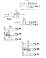
- the present invention is based on an analysis of fault injection mechanisms which will be briefly described in relation with FIGS. 1 to 5.
- the present invention is based on the assumption that any sequential logic circuit comprises a juxtaposition of elementary logic modules having the same general structure, illustrated in FIG. 1.
- the elementary logic module 10 represented in this figure comprises an asynchronous logic block 11 in series with a synchronous flip-flop 12, for example a flip-flop flip-flop (or flip-flop D).
- the flip-flop 12, formed by N flip-flops in parallel of 1 bit each (not shown), comprises an input D of N bits, an output Q of N bits and a synchronization input receiving a clock signal CK0.
- the input D is connected to the output of the block 11 and the output Q provides a synchronous result SR which copies the result R at each edge of the clock signal, for example at each rising edge.
- any logic circuit can be broken down into a plurality of elementary logic modules arranged in series and / or in parallel, each logic module comprising an asynchronous logic block executing a determined logic function.
- the input IN of the logic block 11 of FIG. 1 is presumed to be connected to the Q output of the flip-flop of another elementary logic module
- the output Q of the flip-flop 12 is presumed to be connected to the input IN the asynchronous logic block of another basic logic module.
- This assumption holds true in most logic circuits because the recommendations made by RTL code synthesis tool providers usually lead to such a logical circuit structure, except for primary inputs and outputs. of the logic circuit.
- a fault injection attack in a logic circuit relates to all or part of the elementary logic modules that make up the logic circuit.
- the analysis of the fault injection mechanism and the search for solutions can therefore, according to the invention, be reduced to the scale of an elementary logic module.
- the fault injection attack aims at the synchronous flip-flop 12 or target the asynchronous logic block 11. Each fault injection hypothesis must therefore be considered independently of the other.
- FIG. 2 illustrates a fault injection in the synchronous flip-flop 12.
- Such fault injection is performed on an internal node of the flip-flop and the Q output of the flip-flop provides an erroneous synchronous result #SR.
- the output voltage of the flip-flop is maintained by two inverting doors arranged head-to-tail forming a latch ("latch") and is provided by a comparator arranged to compare at a threshold voltage the voltage present on an internal node of the flip-flop.
- An attack on the internal node causes the appearance of an erroneous value which remains preserved in the latch by the latch formed by the inverting gates.
- FIG. 3 represents a fault injection targeting the asynchronous logic block 11.
- FIGS. 4A-4C and 5A-5C illustrate two distinct scenarios of a fault injection at the input of the flip-flop, due to a fault injection performed in the asynchronous logic block 11 and found in the result R.
- FIGS. 4C illustrate the case of a fault injection having no effect on the synchronous result SR
- FIGS. 5A-5C illustrate the case of a fault injection having an effect on the synchronous result SR.
- FIGS. 4A, 5A show the clock signal CK1
- FIGS. 4B, 5B represent the value of a bit B on an internal node Dint of the flip-flop
- FIGS. 3C, 4C represent the value of the output Q of the FIG. rocker.
- the flip-flop has a Tsetup stabilization window delimited by times ts1 and ts2, the instant ts2 corresponding to the appearance of the rising edge of the clock signal CK1.
- the value of the bit B on the internal node Dint which is the image of the bit applied to the input D, must be stable before the instant ts1 in order to be copied by the output Q at the moment when the rising edge intervenes.
- the internal node Dint of the flip-flop has a logic value transition during which bit B changes from a value B0 to a value B1. The transition from B0 to B1 takes place between instants t1 and t2. Time t2 must occur before time ts1, which marks the beginning of the Tsetup stabilization period.
- an attack of the internal node Dint occurs at a time t3 and ends at a time t4 which precedes the instant ts1.
- the fault injection imposes an erroneous bit # B1 on the node Dint, but ends before the instant ts1, so that the internal node Dint returns to the value B1 (imposed by the input D) before the critical phase Tsetup .
- the fault injection remains ineffective because it is the bit B1 which is copied by the Q output of the flip-flop at time ts2.
- a fault injection # B1 on the node Dint occurs on the contrary between two instants t3 'and t4' located inside the Tsetup window.
- it is the erroneous bit # B1 which is copied by the output Q at the instant ts2, as represented in FIG. 4C.
- the fault injection is also copied at the output when t3 ' ⁇ ts1 and t4'> ts1.
- a fault injection into the flip-flop 12 can be detected by comparing the value on the input D before the rising edge of the clock signal and the value on the output Q after the rising edge of the clock signal.
- a first object of the invention is to provide means for verifying the integrity of a synchronous flip-flop of a logic module, in order to detect fault injection attacks in an internal node of the flip-flop.
- a second object of the invention is to provide means for verifying the integrity of the output of the asynchronous logic block of a logic module, in order to detect fault injection attacks on an internal node of the asynchronous logic block.
- An objective of the invention is achieved by the provision of a logic circuit comprising at least one logic module comprising a functional synchronous flip-flop receiving a functional result comprising several bits in parallel and providing a synchronous result that copies the functional result, and a first one.
- flip-flop integrity control module comprising: a first coding block receiving the functional result and providing a first code of a number of bits less than or equal to the number of bits of the functional result, a second coding block receiving the synchronous result and providing a second code of a number of bits less than or equal to the number of bits of the synchronous result, a non-functional synchronous latch receiving the first code and providing a third code which copies the second code, and a comparator for compare the second code with the third code, and provide a first error signal ayan t an active value when the second code and the third code are not identical.
- the logic circuit comprises a second module for controlling the integrity of the functional flip-flop, comprising: means for providing at least a first reference bit from the functional result, an inverter circuit for providing a first inverted reference bit from the first reference bit, a first non-functional synchronous flip-flop receiving the first reference bit and providing a second reference bit which copies the first reference bit, a second non-functional synchronous flip-flop receiving the first inverted reference bit and providing a third reference bit which copies the first inverted reference bit, a comparator for comparing the second reference bit and the third reference bit and providing a second signal; error having an active value when the second reference bit and the third reference bit are identical.
- the second control module comprises a first coding block receiving all or part of the functional result and providing a code forming the first reference bit.
- the logic circuit comprises a combination of the first control module and the second control module, and a logic gate to combine the first error signal and the second error signal and to provide an error signal.
- a logic gate to combine the first error signal and the second error signal and to provide an error signal. general having an active value when at least the first or second error signal has the active value.
- the means for supplying at least the reference bit of the second module is the first coding block of the first control module.
- the logic circuit comprises a functional asynchronous logic block executing a determined logical function and comprising at least one data input and an output providing the functional result, and a third module for checking the integrity of the functional logic block.
- a functional asynchronous logic block executing a determined logical function and comprising at least one data input and an output providing the functional result
- a third module for checking the integrity of the functional logic block comprising: a non-functional asynchronous logic block performing the same logic function as the functional logic block, comprising at least one data input and one output providing a non-functional result, non-functional synchronous latches for applying to the input of the non-functional logic block data present at the input of the functional logic block, and means for comparing the functional result and the non-functional result and providing a third error signal having an active value when the functional result and the non-functional result are not identical.
- the third control module comprises: a first coding block receiving the synchronous result and providing a first output code comprising a number of bits less than or equal to the number of bits of the synchronous result, a second coding block receiving the non-functional result and providing a second output code comprising a number of bits less than or equal to the number of bits of the non-functional result, and a comparator for comparing the first output code and the second output code, and providing the third error signal.
- the non-functional logic block is a reduced logic block which comprises at least one reduced input and one reduced output each comprising a number of bits less than the corresponding input and the corresponding output of the functional logic block, and which performs the same logic function with respect to its inputs as the functional logic block
- the third control module comprises: at least one coding block connected as input to the input of the functional logic block, providing an input code which is applied at the reduced input of the non-functional logic block via the non-functional latches, a coding block receiving the synchronous result and providing a first output code comprising a number of bits less than or equal to the number of bits of the synchronous result, and a comparator having an input receiving the first output code and a another input connected to the output of the non-functional logic block, to provide the third error signal.
- the non-functional logic block provides a non-functional result that is directly applied to the comparator to be compared to the first output code.
- the non-functional logic block provides a non-functional result that is applied to the input of a code block whose output provides a second output code that is applied to the comparator to be compared to the first code of the code. exit.
- the functional logic block comprises at least one control input receiving a control signal comprising one or more bits
- the non-functional logic block comprises a control input which receives the control signal via a control signal.
- the coding blocks are logic circuits each providing a parity bit.
- the coding blocks are circuits providing a Hamming code.
- the functional and non-functional flip-flops are driven by the same clock signal.
- the functional flip-flops are controlled by a first clock signal and the non-functional flip-flops are controlled by a second clock signal which is fed to the non-functional flip-flops by a specific clock path.
- the logic circuit comprises: a plurality of logic modules, a plurality of control modules each associated with a logic module, and each providing an error signal, and logic gates for collecting the signals provided by the plurality of control modules, and provide a general error signal.
- a logic circuit can be broken down into a plurality of elementary logic modules.
- the present invention proposes to associate an individual integrity control module with each elementary logic module to be protected against a fault injection attack.
- Logic modules protected by integrity control modules may represent only a part of the logic circuit to be secured, in particular parts that are most sensitive to fault injection. It is up to those skilled in the art to determine, when designing such a logic circuit, which elementary logic modules must be provided with an integrity control module.
- the module 10 is here a volatile register element provided for storing an 8-bit data (byte) and comprises an asynchronous logic block 11 providing an 8-bit result R and a synchronous flip-flop 12 comprising 8 elementary synchronous flip-flops of 1 bit each. (not shown) arranged in parallel and controlled by a clock signal CK1.
- the result R is applied to the input D of the flip-flop 12 whose Q output provides a synchronous result SR.
- Block 11 here comprises a multiplexer MUX and an XOR gate (exclusive) and has four data inputs IN0, IN1, IN2, IN3 of 8 bits each, and a control input INC of 2 bits.
- the multiplexer MUX has a first 8-bit data input forming the input IN0 of the block 11, a second data input connected to the output of the XOR gate, a third data input forming the input IN3 of the block as well as a control input forming the control input INC of the block 11.
- the XOR gate formed by 8 elementary XOR gates each having two 1-bit inputs (not shown), comprises an 8-bit input forming the input IN1 of the block 11 and an 8-bit input forming the input IN2 of the block 11.
- the output of the XOR gate provides the multiplexer with an 8-bit word of data, each bit of which is the result of the bit-wise combination of the bits of the same rank present on each of the inputs of the XOR gate.
- the first input of the multiplexer forming the input IN0 of the block is connected to the output Q of the flip-flop 12, and receives the result SR.
- This input connected to the output of the logic module 10 makes it possible to refresh the value of the volatile register at each clock cycle, when no new data is recorded therein.
- the result R provided by the logic block 11 as well as the synchronous result at the output of the module 10 depend on the bits applied to the control input INC and may be equal to the word present on the input IN0, to the word provided by the XOR gate (bitwise combination by the XOR function of the IN1, IN2 inputs) or the word present on the IN3 input.
- asynchronous flip-flop integrity control module 12 Examples of embodiments of a synchronous flip-flop integrity control module 12 will now be described, and examples of embodiments of a synchronous flip-flop 12 will be described.
- asynchronous logic block integrity check module 11 asynchronous logic block integrity check module 11.
- control modules In the following, such integrity control modules according to the invention will be called “control modules”, being extended that the control in question is an integrity check.
- the elements of a basic logic module and the elements of a control module will be respectively called “functional” elements and “non-functional” elements in order to distinguish them.
- the terms “functional” or “non-functional” only mean that the element concerned belongs to a basic logic module to be controlled or to a control module associated with the elementary logic module.
- the constituent elements of the module 10 described above, forming a register element are all functional elements.
- FIG. 6 represents, in addition to the module 10, a control module 20 according to the invention, intended to detect fault injection attacks in the functional flip-flop 12 of the module 10.
- the module 20 comprises two coding blocks 21, 22, a non-functional synchronous flip-flop 23 driven by a clock signal CK2, a comparator 24 with two inputs and, optionally, a non-functional synchronous flip-flop 25 represented in dashed lines, also driven. by the signal CK2.
- each coding block 21, 22 respectively receive the result R provided by the asynchronous logic block 11 and the synchronous result SR supplied by the synchronous flip-flop 12. They respectively provide a code C1 and a code C2, here the codes 1 bit each.
- the codes C1, C2 are, for example, parity codes.
- each coding block 21, 22 comprises an XOR gate tree (not shown).
- the block 21 comprises a first gate XOR receiving two first bits of the result R, a second gate XOR receiving the third bit of the result R and the output of the first gate XOR, a third gate XOR receiving the fourth bit of the result R and the output of the second XOR gate, and so on.
- the code C1 is applied to an input D of the non-functional flip-flop 23, the output Q of which provides a code C3.
- the codes C1, C3 are applied to the inputs of the comparator 24.
- the comparator 24 for example an XOR gate, provides an error signal ER1 which is at 0 when the two codes are equal and is at 1 (active value) when the two codes are different.
- the flip-flop 25 receives the error signal ER1 and provides a synchronized error signal SER1.
- the clock signal CK1 applied to the functional flip-flop 12 and the clock signal CK2 applied to the non-functional flip-flops 23, 25 are assumed to be identical and synchronous, and come from the same clock signal source.
- the path leading the signal CK1 to the functional flip-flop and the path leading the signal CK2 to the non-functional flip-flops may be different.
- the clock paths comprise separate conductive tracks connected to the same clock signal source and present substantially the same temporal properties (phase shift between the incoming clock signal and the outgoing clock signal) so that the switching of functional and non-functional flip-flops is substantially at the same time, a small time shift can however be tolerated.
- the module 20 makes it possible to detect an error injection attack in the functional flip-flop 12, which affects the synchronous result SR while the result R applied to the input of the flip-flop 12 is valid.
- the value of the result SR is different from that of the result R
- the codes C1 and C2 are different
- the codes C2 and C3 are also different because the code C3 copies the code C2.
- the ER1 error signal thus passes to 1.
- the flip-flop 25 may be arranged outside the control module and be a collective synchronization flip-flop receiving the result of the combination of several error signals emitted by various control modules according to the invention, as will be described later. .
- FIG. 7 represents a second embodiment of a control module 30 according to the invention.
- the module 30 comprises an encoding block 31, an inverting gate 32, two flip-flops 33, 34 driven by the clock signal CK2, and a comparator 35.
- the coding block 31 receives as input the result R provided by the logic block asynchronous 11 of the logic module 10.
- the output of the block 31 provides a reference bit C4, here a parity code of 1 bit.
- the reference bit C4 is applied to the inverting gate 32 and to an input D of the flip-flop 33.
- the input D of the flip-flop 34 is connected to the output of the inverting gate 32, which provides an inverted reference bit / C4 .
- the outputs of the flip-flops 33, 34 respectively provide bits C5, C6 synchronized with the clock signal CK2 and assumed to be different relative to each other since the bit C5 is derived from the bit C4 while the bit C6 is derived from the bit inverted / C4.
- the bits C5, C6 are applied at the input of the comparator 35, here an NXOR gate (No or Exclusive).
- the comparator provides an error signal ER2 which is equal to 0 when the bits C5, C6 are different, and which is equal to 1 (active value) if the two bits are equal.
- the module 30 makes it possible to detect a fault injection attack of the "all-0" or "all-1" type. Such a fault injection targets all the latches of the same zone of a logic circuit. In this case, the bits C5 and C6 are equal and the signal ER2 goes to 1.
- the reference bit C4 can be obtained from various other ways than the one described above.
- the reference bit is for example one of the bits of the result R, or is provided by a logic gate receiving all or part of the bits constituting the result R. Several reference bits may also be provided.
- FIG. 8 represents a control module 40 comprising a combination of the two control modules previously described.
- the module 40 thus comprises the elements of the module 30, namely the coding block 31, the inverting gate 32, the gates 33, 34, and the comparator 35 whose output provides the ER2 error signal.
- the module 40 also comprises elements of the module 20, namely the coding block 22 and the comparator 24 whose output provides the error signal ER1.
- the block 31 and the flip-flop 33 are pooled and provide both the bit C5 applied to the comparator 35 and the code C3 applied to the comparator 24 (the bit C5 and the code C3 being identical when the coding blocks provide a bit of parity).
- Block 40 also includes an OR gate 41 which receives the ER1, ER2 error signals as input and provides a general ER12 error signal. Thus, if one of the two error signals goes to 1 (fault injection in the functional flip-flop 12 or fault injection by setting all the flip-flops to 0 or 1), the general error signal ER12 goes to 1.
- the implementation of the present invention in a complex logic circuit comprises the provision of a control module according to the invention (20, 30 or 40 ) for each logic module to be secured against fault injection into the logic circuit.
- FIG. 9 very schematically represents the general architecture of an integrity control device 100 according to the invention.
- the device is organized in blocks BL0 ... BLn, each block comprising sub-blocks SBL0 ... SBLm, each sub-block comprising modules of control M0 ... Mk, each control module being associated with a basic logic module of the logic circuit to be secured (not shown).
- an OR logic gate 101 collects the individual error signals from the control modules, to obtain sub-block error signals ER0, 0 ... ER0, m.
- ER0, m are gathered by an OR gate 102 which supplies a block error signal ER0 ... ERn.
- the block error signals are themselves collected by OR gates in cascades schematized in the figure by an OR gate 103 with multiple inputs.
- the output of gate 103 provides a general error signal GER applied to a termination synchronous flip-flop 104 which provides a synchronous general error signal SGER.
- This general error signal can be used in various ways within the reach of those skilled in the art to block the logic circuit under control, especially during the execution of a so-called sensitive operation.
- Those skilled in the art are also able to provide various other ways of producing the general error signal from error signals from control modules, and various ways of locking this general error signal when an error is detected at a control module.
- Those skilled in the art are also able to predict the conditions for resetting the general error signal, for example resetting (RESET) or power down ("power down”) of the logic circuit.
- RESET resetting
- power down power
- FIG. 10 represents a control module 50 according to the invention, connected to a logic module 10 comprising an asynchronous logic block 11 and a synchronous flip-flop 12.
- the output of the block 11 provides as previously a result R on the input D of the flip-flop 12, whose output provides the synchronous result SR.
- the block 11 here comprises data inputs IN0, IN1 ... INn and a control input INC.
- the input IN0 is here connected to the output Q of the flip-flop 12, and receives the synchronous result SR.
- the results R and SR are for example here 8-bit words.
- the module 50 comprises a non-functional logic block 51 and synchronous flip-flops 52-0, 52-1, ... 52-n, 52-C.
- the non-functional logic block 51 is the image of the functional logic block 11 and has inputs IN0 ', IN1' ... INn ', INC' identical to the inputs IN0, IN1 ... INn, INC 'of block 11.
- Sa output provides a synchronous non-functional result SR 'by applying the same asynchronous logic function as the function block 11.
- the inputs IN0' to INn ', INC' are connected to the corresponding inputs of the block 11 via the flip-flops 52-0, 52-1, ... 52-n, 52-C.
- the input IN0 ' is connected to the input IN0 via the flip-flop 52-0
- the input IN1' is connected to the input IN1 via the flip-flop 52-1
- the input INn ' is connected to the input INn via the flip-flop 52-n
- the input INC' is connected to the input INC via the flip-flop 52-C-.
- the non-functional flip-flops 52-0 to 52-n, 52-C are driven by the clock signal CK2 described above.
- Each flip-flop 52 comprises a number of elementary flip-flops (1-bit flip-flops) equal to the number of bits that presents the corresponding input of the non-functional logic block 51.
- the non-functional logic block 51 thus provides, with a shift of 1 clock cycle, a presumed result SR 'identical to the synchronous result SR at the output of the flip-flop 12.
- the module 50 also comprises a comparator 55, for example a XOR gate with two inputs, here two inputs of 8 bits each, the first input receiving the non-functional synchronous result SR 'and the second input receiving the functional synchronous result SR.
- the comparator 55 provides an error signal ER3 which is equal to 1 (active value) when the results SR, SR 'are different.
- coding blocks 53, 54 are arranged at the input of the comparator 55.
- the coding block 53 receives the non-functional result SR 'and provides on the first input of the comparator 55 a code C10 which is a function of SR ', here a code of 1 bit, for example a parity code.
- Block 54 identical to block 53, receives the functional result SR and supplies a code C11, here of 1 bit, for example a parity code, on the second input of the comparator.
- the comparator 55 is for example an elementary XOR gate with two inputs of 1 bit each.
- the module 50 makes it possible to detect an error injection attack in the functional logic block 11, which affects the result R while the inputs IN0-INn, INC are assumed to be valid. In such a case, the value of the synchronous result SR is different from that of the non-functional result R, the codes C10 and C11 are different, and the error signal ER3 goes to 1.
- the erroneous functional result #RVAL which appears at the instant T1 + ta at the output of the functional block, propagates at the output of the functional flip-flop 12 at the time T2 while at the same time the inputs IN0-INn, INC, which are valid, are sampled by the non-functional flip-flops 52-0 to 52-n, 52-C at the input of the non-functional block 51.
- the erroneous result #RVAL then propagates to the output of the coding block 54 to T2 + ta to form an erroneous code C11 (P (#RVAL)) while at the same time the non-functional result not erred RVAL is established at the output of the block 51.
- the code C10 is established at the output of the block 53 and at the time T2 + 3ta the ER3 error signal goes to 1.
- a synchronization flip-flop of the signal ER3 can be arranged at the output of the comparator 55.
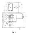
- This second embodiment of a control module 60 aims to significantly reduce the size and bulk of the non-functional logic block.
- the non-functional logic block 51 described above is replaced by a reduced logic block 61 which performs the same logic function as the function block 11 but with a smaller number of bits at the input and at the output.
- the block 61 has reduced inputs IN0 ", IN1"... INn "each having a number of bits in parallel less than that of the inputs IN0, IN1 ... INn of the functional block 11.
- block 61 nevertheless has a control input INC "identical to the input INC of block 11, in order to perform the same logic function, because the number of control bits can not be reduced.
- the reduced inputs are, for example, 1-bit inputs instead of 8-bits.
- the non-functional flip-flops 52-0 to 52-n, 52-C of the previous embodiment which were 8-bit flip-flops (each comprising 8 1-bit elementary flip-flops), are replaced by flip-flops 62-0 to 62-. n of 1 bit each, or elementary latches, always driven by the clock signal CK2.
- the flip-flop 52-C is retained because the control input INC is not reduced.
- the module 60 further comprises coding blocks 63-0, 63-1, ... 63-n arranged between the inputs IN0, IN1, ... INC of the functional block 11 and the inputs D of the flip-flops 62-0. 62-1, ... 62-n.
- the coding blocks provide reduced input codes RC0, RC1 ... RCn having a number of bits corresponding to the number of bits of the inputs IN0 ', IN1' ... INn 'of the reduced logic block 61.
- These reduced codes are here codes of 1 bit each, for example parity bits.
- the output of the block 61 provides the transform of the parity bits RC0, RC1 ... RCn by the logic function of the block, ie the parity code of the transform of the inputs not reduced by the logic function of the block.
- the output of the block 61 directly supplies the code C10 described above, which is applied to the comparator 55.
- the code C11 is taken here at the output of the coding block 63-0, which here receives the synchronous result SR (because the Synchronous result SR of the logic module 10 is brought back to the functional input IN0 of the logic block 11 and is therefore also brought back to the coding block 63-0).
- the result ER3 is therefore identical to that previously described (see table 2).
- the size of the non-functional logic block 61 is here reduced by 8 relative to that of the non-functional logic block 51.
- the control module 70 shown in FIG. 12 is an intermediate embodiment between the two embodiments previously described. It comprises a reduced logic block 71 comprising inputs IN0 "', IN1"' ... INn "'each having a number of bits in parallel which is greater than the number of bits of the inputs IN0", IN1 "... INn” the non-functional block 61 (FIG 11) but is smaller than the number of bits of the inputs INO, IN1 ... INn of the functional block 11, for example 2 bits. Coding blocks 63-0 to 63-n are replaced by coding blocks 73-0 to 73-n providing an appropriate number of bits. The flip-flops 62-0 to 62-n are replaced by flip-flops 72-0 to 72-n each capable of receiving a suitable number of bits.
- the output of the block 71 provides a code C10 'which comprises a number of bits in parallel greater than that of the code C11, which is again provided here by the coding block 54 previously described.
- the output of the block 71 is applied to a coding block 74 which reduces the number of bits of the code C10 'to provide the code C10 comprising a number of bits identical to that which comprises the code C11, for example 1 bit.
- the codes C10, C11 are applied as previously to the comparator 55, to obtain the ER3 error signal.
- FIG. 13 represents a control module 80 which represents the combination of all the aspects of the invention described above.
- the module 80 is associated here with the elementary logic module 10 forming a register element, the structure of which has already been described.
- the functional logic block 11 thus comprises the MUX multiplexer and the XOR gate, the synchronous result SR being brought back to the IN0 input of the multiplexer.
- the module 80 comprises the module 40 already described, which will not be described again, the same elements being designated by the same references.
- the module 40 itself comprises a combination of the modules 20, 30 previously described.
- the module 80 also includes the module 60 whose general structure has also been previously described.
- the non-functional logic block 61 of the module 60 here comprises an IMUX reduced multiplexer comprising only three data inputs of 1 bit each, and a reduced XOR gate, designated IXOR, comprising only two inputs of 1 bit each.
- the module 60 also comprises non-functional synchronous flip-flops 62-0, 62-1, 62-2, 62-3 of 1 bit each, a non-functional synchronous flip-flop 62-C of two bits, and coding blocks 63-1. , 63-2, 63-3 having 8 bits at the input and 1 bit at the output, here parity calculation blocks (XOR gate trees).
- the 2-bit control input of the multiplexer MUX is connected to the 2-bit control input of the IMUX multiplexer via flip-flop 62-C.
- the 8-bit IN1, IN2, IN3 inputs of the functional logic block 11 are connected to the inputs of the coding blocks 63-1, 63-2, 63-3, respectively.
- the outputs of the coding blocks 63-1, 63-2, 63-3, of 1 bit each, are connected to the corresponding inputs of the non-functional block 61 via the non-functional flip-flops 62-1, 62-2, 62 -3, respectively.
- the coding block 22 of the module 40 is here used as coding block 63-0 of the module 60, so that the code C2 of the module 40 also forms the code C11 of the module 60.
- the code C11 is applied to an input of the comparator 55 which receives on its other input the output of the reduced multiplexer IMUX, the code C10. Code C11 is also applied to the first input of the IMUX multiplexer via flip-flop 62-0.
- the module 80 comprises an OR gate 81 which receives the ER12 error signal from the module 40 and the error signal ER3 of the module 60, and which provides a general error signal ER123 which passes to 1 since an attack is detected in the functional flip-flop 12 and / or in the functional logic block 11. As indicated above, this signal can be combined with signals of other modules to form a subgroup signal, itself combined to other subgroup signals for forming group signals, etc., until a general error signal is obtained for the whole of a complex logic circuit.
- the coding blocks which allow a reduction in the number of bits for the comparison of the functional and non-functional results, can be of any known type, in particular coding blocks supplying Hamming codes which are, like the parity codes. , commonly used in data security methods.
Landscapes
- Engineering & Computer Science (AREA)
- Computer Security & Cryptography (AREA)
- Software Systems (AREA)
- Theoretical Computer Science (AREA)
- Computer Hardware Design (AREA)
- Physics & Mathematics (AREA)
- General Engineering & Computer Science (AREA)
- General Physics & Mathematics (AREA)
- Logic Circuits (AREA)
Claims (16)
- Logikschaltung, die mindestens ein Logikmodul (10) umfasst, das einen funktionalen synchronen Flip-Flop (12) umfasst, der ein funktionales Ergebnis (R) empfängt, das mehrere Bits parallel umfasst und ein synchrones Ergebnis (SR) liefert, das das funktionale Ergebnis (R) kopiert,
dadurch gekennzeichnet, dass sie ein erstes Steuermodul (20) der Integrität des funktionalen Flip-Flops umfasst, enthaltend:- einen ersten Codierungsblock (21), der das funktionale Ergebnis (R) empfängt und einen ersten Code (C1) mit einer Anzahl von Bits liefert, die kleiner oder gleich der Anzahl von Bits des funktionalen Ergebnisses (R) ist,- einen zweiten Codierungsblock (22), der das synchrone Ergebnis (SR) empfängt und einen zweiten Code (C2) mit einer Anzahl von Bits liefert, die kleiner oder gleich der Anzahl von Bits des synchronen Ergebnisses ist,- einen synchronen nicht funktionalen Flip-Flop (23) der den ersten Code (C1) empfängt und einen dritten Code (C3) liefert, der den zweiten Code (C2) kopiert, und- einen Komparator (24), um den zweiten Code (C2) mit dem dritten Code (C3) zu vergleichen und ein erstes Fehlersignal (ER1) zu liefern, das einen aktiven Wert hat, wenn der zweite Code und der dritte Code nicht identisch sind. - Logikschaltung nach Anspruch 1, die ein zweites Modul (30) zum Steuern der Integrität des funktionalen Flip-Flops (12) umfasst, enthaltend:- ein Mittel (31), um mindestens ein erstes Referenzbit (C4) ausgehend von dem funktionalen Ergebnis (R) zu liefern,- eine Umkehrschaltung (32), um ein erstes umgekehrtes Referenzbit (/C4) ausgehend von dem ersten Referenzbit (C4) zu liefern,- einen ersten synchronen nicht funktionalen Flip-Flop (33), der das erste Referenzbit (C4) empfängt und ein zweites Referenzbit (C5) liefert, das das erste Referenzbit (C4) kopiert,- einen zweiten nicht funktionalen synchronen Flip-Flop (34), der das erste umgekehrte Referenzbit (/C4) empfängt und ein drittes Referenzbit (C6) liefert, das das erste umgekehrte Referenzbit (/C4) kopiert, und- einen Komparator (35), um das zweite Referenzbit (C5) und das dritte Referenzbit (C6) zu vergleichen und ein zweites Fehlersignal (ER2) zu liefern, das einen aktiven Wert hat, wenn das zweite Referenzbit und das dritte Referenzbit identisch sind.
- Logikschaltung nach Anspruch 2, bei der das zweite Steuermodul (30) einen ersten Codierungsblock (31) umfasst, der alles oder einen Teil des funktionalen Ergebnisses (R) empfängt und einen Code (C1) liefert, der das erste Referenzbit bildet.
- Logikschaltung nach einem der Ansprüche 2 und 3, die eine Kombination (40) des ersten Steuermoduls und des zweiten Steuermoduls umfasst, und ein Logikgatter (41), um das erste Fehlersignal (ER1) und das zweite Fehlersignal (ER2) zu kombinieren und ein allgemeines Fehlersignal (ER12) zu liefern, das einen aktiven Wert hat, wenn mindestens das erste oder das zweite Fehlersignal den aktiven Wert hat.
- Logikschaltung nach Anspruch 4, bei der das Mittel (31) zum Liefern mindestens des Referenzbits des zweiten Moduls (30) der erste Codierungsblock (21) des ersten Steuermoduls (20) ist.
- Logikschaltung nach einem der Ansprüche 1 bis 5, die einen funktionalen asynchronen Logikblock (11) umfasst, der eine bestimmte Logikfunktion durchführt und mindestens einen Dateneingang (IN0-INn) umfasst und einen Ausgang, der das funktionale Ergebnis (R) liefert, und ein drittes Steuermodul (50, 60, 70) der Integrität des funktionalen Logikblocks (11), umfassend:- einen nicht funktionalen asynchronen Logikblock (51, 61, 71), der die gleiche Logikfunktion ausführt wie der funktionale Logikblock, der mindestens einen Dateneingang (IN0'-INn', IN0"-INn", IN0"'-INn"') und einen Ausgang umfasst, der ein nicht funktionales Ergebnis (SR', C10, C10') liefert,- nicht funktionale synchrone Flip-Flops (52, 62, 72), um an den Eingang (IN0'-INn', IN0"-INn", IN0"'-INn"') des nicht funktionalen Logikblocks Daten anzulegen, die am Eingang (IN0-INn) des funktionalen Logikblocks gegenwärtig sind, und- Mittel (53, 54, 55, 63-0, 74, 75), um das funktionale Ergebnis (R) und das nicht funktionale Ergebnis (SR', C10, C10') zu vergleichen und ein drittes Fehlersignal (ER3) zu liefern, das einen aktiven Wert hat, werin das funktionale Ergebnis und das nicht funktionale Ergebnis nicht identisch sind.
- Logikschaltung nach Anspruch 6, bei der das dritte Steuermodul (50) Folgendes umfasst:- einen ersten Codierungsblock (54), der das synchrone Ergebnis (SR) empfängt und einen ersten Ausgangscode (C11) liefert, der eine Anzahl von Bits aufweist, die kleiner oder gleich der Anzahl von Bits des synchronen Ergebnisses ist,- einen zweiten Codierungsblock (53), der das nicht funktionale Ergebnis (SR', C10') empfängt und einen zweiten Ausgangscode (C10) liefert, der eine Anzahl von Bits umfasst, die kleiner oder gleich der Anzahl von Bits des nicht funktionalen Ergebnisses ist, und- einen Komparator (55), um den ersten Ausgangscode und den zweiten Ausgangscode zu vergleichen und das dritte Fehlersignal (ER3) zu liefern.
- Logikschaltung nach Anspruch 6, bei der der nicht funktionale Logikblock ein reduzierter Logikblock (61, 71) ist, der mindestens einen reduzierten Eingang (IN0"-INn"', IN0"'-INn"') und einen reduzierten Ausgang umfasst, die jeweils eine kleinere Anzahl von Bits am entsprechenden Eingang und am entsprechenden Ausgang des funktionalen Logikblocks (11) umfassen und in Bezug auf ihre Eingänge die gleiche Logikfunktion ausführt wie der funktionale Logikblock, und bei der das dritte Steuermodul (60, 70) Folgendes umfasst:- mindestens einen Codierungsblock (63-0 bis 63-n, 73-0 bis 73-n,), der am Eingang mit dem Eingang (IN0-INn) des funktionalen Logikblocks (11) verbunden ist, der einen Eingangscode (RC0-RCn) liefert, der an den reduzierten Eingang (INO"'-INn"', IN0"'-INn des nicht funktionalen Logikblocks (61, 71) über nicht funktionale Flip-Flops (62, 72) anlegt wird,- einen Codierungsblock (63-0, 54), der das synchrone Ergebnis (SR) empfängt und einen ersten Ausgangscode (C11) liefert, der eine Anzahl von Bits umfasst, die kleiner oder gleich der Anzahl von Bits des synchronen Ergebnisses (SR) ist, und- einen Komparator (55), der einen Eingang hat, der den ersten Ausgangscode (C11) empfängt, und einen anderen Eingang, der mit dem Ausgang des nicht funktionalen Logikblocks (61, 71) verbunden ist, um das dritte Fehlersignal (ER3) zu liefern.
- Logikschaltung nach Anspruch 8, bei der der nicht funktionale Logikblock (61) ein nicht funktionales Ergebnis (C10) liefert, das direkt an den Komparator (55) angelegt wird, um mit dem ersten Ausgangscode (C11) verglichen zu werden.
- Logikschaltung nach Anspruch 8, bei der der nicht funktionale Logikblock (71) ein nicht funktionales Ergebnis (C10') liefert, das an den Eingang eines Codierungsblocks (74) angelegt wird, dessen Ausgang einen zweiten Ausgangscode (C10) liefert, der an den Komparator (55) angelegt wird, um mit dem ersten Ausgangscode (C11) verglichen zu werden.
- Logikschaltung nach einem der Ansprüche 6 bis 10, bei der:- der funktionale Logikblock (11) mindestens einen Steuereingang (INC) umfasst, der ein Steuersignal empfängt, das ein oder mehrere Bits enthält, und- der nicht funktionale Logikblock einen Steuereingang (INC', INC", INC"') umfasst, der das Steuersignal über einen nicht funktionalen synchronen Flip-Flop (52-C) empfängt.
- Logikschaltung nach einem der Ansprüche 1 bis 11, bei der die Codierblöcke Logikschaltungen sind, die jede ein Paritätsbit liefern.
- Logikschaltung nach einem der Ansprüche 1 bis 11, bei der die Codierblöcke Schaltungen sind, die einen Hamming-Code liefern.
- Logikschaltung nach einem der Ansprüche 1 bis 13, bei der die funktionalen und nicht funktionalen Flip-Flops von dem gleichen Taktgebersignal gesteuert werden.
- Logikschaltung nach einem der Ansprüche 1 bis 13, bei der die funktionalen Flip-Flops von einem ersten Taktgebersignal (CK1) gesteuert werden, und die nicht funktionalen Flip-Flops von einem zweiten Taktgebersignal (CK2) gesteuert werden, das von einem spezifischen Taktgeberpfad bis zu den nicht funktionalen Flip-Flops geleitet wird.
- Logikschaltung nach einem der Ansprüche 1 bis 15, umfassend:- eine Vielzahl von Logikmodulen,- eine Vielzahl von Steuermodulen, die jeweils einem Logikmodul zugewiesen sind und jeweils ein Fehlersignal liefern, und- Logikgatter (102, 103), um die Fehlersignale zu vereinen, die von der Vielzahl von Steuermodulen geliefert werden und um ein allgemeines Fehlersignal zu liefern.
Applications Claiming Priority (2)
| Application Number | Priority Date | Filing Date | Title |
|---|---|---|---|
| FR0402160A FR2867326A1 (fr) | 2004-03-02 | 2004-03-02 | Dispositif de protection contre l'injection d'erreur dans une bascule synchrone d'un module logique elementaire |
| FR0402160 | 2004-03-02 |
Publications (2)
| Publication Number | Publication Date |
|---|---|
| EP1571754A1 EP1571754A1 (de) | 2005-09-07 |
| EP1571754B1 true EP1571754B1 (de) | 2006-07-12 |
Family
ID=34746481
Family Applications (1)
| Application Number | Title | Priority Date | Filing Date |
|---|---|---|---|
| EP20050001617 Expired - Fee Related EP1571754B1 (de) | 2004-03-02 | 2005-01-27 | Gerät zum Schutz eines synchronen Flip-Flops eines elementaren Logikmoduls gegen Fehlerinjektionen |
Country Status (3)
| Country | Link |
|---|---|
| EP (1) | EP1571754B1 (de) |
| DE (1) | DE602005000038T2 (de) |
| FR (1) | FR2867326A1 (de) |
Families Citing this family (1)
| Publication number | Priority date | Publication date | Assignee | Title |
|---|---|---|---|---|
| CN113656230B (zh) * | 2021-08-20 | 2023-06-16 | 地平线(上海)人工智能技术有限公司 | 故障诊断电路、方法、装置及计算机可读存储介质 |
Family Cites Families (4)
| Publication number | Priority date | Publication date | Assignee | Title |
|---|---|---|---|---|
| JPS592057B2 (ja) * | 1979-02-07 | 1984-01-17 | 株式会社日立製作所 | エラ−訂正・検出方式 |
| GB2295753B (en) * | 1992-09-17 | 1996-10-16 | Sony Uk Ltd | Data coding |
| JP2830822B2 (ja) * | 1996-02-09 | 1998-12-02 | 日本電気株式会社 | 高速通信における誤り訂正方法 |
| US5996104A (en) * | 1996-09-13 | 1999-11-30 | Herzberg; Hanan | System for coding system |
-
2004
- 2004-03-02 FR FR0402160A patent/FR2867326A1/fr not_active Withdrawn
-
2005
- 2005-01-27 DE DE200560000038 patent/DE602005000038T2/de active Active
- 2005-01-27 EP EP20050001617 patent/EP1571754B1/de not_active Expired - Fee Related
Also Published As
| Publication number | Publication date |
|---|---|
| EP1571754A1 (de) | 2005-09-07 |
| DE602005000038T2 (de) | 2006-12-28 |
| DE602005000038D1 (de) | 2006-08-24 |
| FR2867326A1 (fr) | 2005-09-09 |
Similar Documents
| Publication | Publication Date | Title |
|---|---|---|
| EP2280364B1 (de) | Fehlerinjektionsdetektor in einer integrierten Schaltung | |
| EP3457620A1 (de) | Ausführungsverfahren eines binären codes einer durch einen mikroprozessor gesicherten funktion | |
| Rührmair et al. | Power and timing side channels for PUFs and their efficient exploitation | |
| EP3712795B1 (de) | Verfahren zur ausführung eines binärcodes durch einen mikroprozessor, der eine ruffunktion und eine aufgerefune funktion enthält | |
| EP3712794B1 (de) | Verfahren zur ausführung eines binärcodes von einem mikroprozessor gesicherten funktion | |
| CA2732651C (fr) | Procede de test de la resistance d'un circuit integre a une analyse par canal auxiliaire | |
| WO2010018071A1 (fr) | Procede de detection d'anomalies dans un circuit de cryptographie protege par logique differentielle et circuit mettant en oeuvre un tel procede | |
| FR2831971A1 (fr) | Procede de memorisation de donnees avec correction d'erreur | |
| FR2843466A1 (fr) | Procede pour empecher la falsification d'un systeme de traitement de donnees, et ce systeme | |
| EP1571522A1 (de) | Vorrichtung zum Schutz gegen Fehlerinjektion in einem asynchronen logischen Block aus einem Logischen Modul | |
| EP3457621B1 (de) | Ausführungsverfahren eines binärcodes einer durch einen mikroprozessor gesicherten funktion | |
| EP3610372B1 (de) | Verfahren zum ausführen eines maschinencodes einer sicheren funktion | |
| EP1571754B1 (de) | Gerät zum Schutz eines synchronen Flip-Flops eines elementaren Logikmoduls gegen Fehlerinjektionen | |
| EP1986137A2 (de) | Verfahren und Vorrichtung zur Überprüfung der Integrität eines logischen Signals, insbesondere eines Uhrsignals | |
| FR2949010A1 (fr) | Procede de contremesure pour proteger des donnees memorisees | |
| FR2897439A1 (fr) | Circuit elelctronique comprenant un mode de test securise par l'utilisation d'un identifiant, et procede associe | |
| EP1710700A2 (de) | Sicherer Co-Prozessor mit Mitteln zur Verhinderung des Zugriffs auf einer Co-prozessoreinheit | |
| FR2828601A1 (fr) | Ensemble de circuits electroniques comportant des moyens de decontamination de parties contaminees par des erreurs | |
| WO2001084491A2 (fr) | Procede de contre mesure dans un microcircuit et carte a puce comportant ledit microcircuit | |
| EP2656534B1 (de) | Verfahren zur multimodalen authentifizierung und erzeugung eines kryptografischen schlüssels anhand von sicheren generalisierten skizzen | |
| EP3832947B1 (de) | Verfahren zur ausführung eines computerprogramms durch ein elektronisches gerät | |
| EP4089557A1 (de) | Verfahren zur ausführung eines binären codes durch einen mikroprozessor | |
| FR3122754A1 (fr) | Microprocesseur équipé d'une unité arithmétique et logique et d'un module matériel de sécurisation | |
| FR2969874A1 (fr) | Procede de reconstruction d'une mesure de reference d'une donnee confidentielle a partir d'une mesure bruitee de cette donnee | |
| FR2830972A1 (fr) | Architecture de circuits protegee contre des perturbations |
Legal Events
| Date | Code | Title | Description |
|---|---|---|---|
| PUAI | Public reference made under article 153(3) epc to a published international application that has entered the european phase |
Free format text: ORIGINAL CODE: 0009012 |
|
| AK | Designated contracting states |
Kind code of ref document: A1 Designated state(s): AT BE BG CH CY CZ DE DK EE ES FI FR GB GR HU IE IS IT LI LT LU MC NL PL PT RO SE SI SK TR |
|
| AX | Request for extension of the european patent |
Extension state: AL BA HR LV MK YU |
|
| GRAP | Despatch of communication of intention to grant a patent |
Free format text: ORIGINAL CODE: EPIDOSNIGR1 |
|
| 17P | Request for examination filed |
Effective date: 20060209 |
|
| AKX | Designation fees paid |
Designated state(s): DE FR GB IT |
|
| GRAS | Grant fee paid |
Free format text: ORIGINAL CODE: EPIDOSNIGR3 |
|
| GRAA | (expected) grant |
Free format text: ORIGINAL CODE: 0009210 |
|
| AK | Designated contracting states |
Kind code of ref document: B1 Designated state(s): DE FR GB IT |
|
| PG25 | Lapsed in a contracting state [announced via postgrant information from national office to epo] |
Ref country code: IT Free format text: LAPSE BECAUSE OF FAILURE TO SUBMIT A TRANSLATION OF THE DESCRIPTION OR TO PAY THE FEE WITHIN THE PRESCRIBED TIME-LIMIT;WARNING: LAPSES OF ITALIAN PATENTS WITH EFFECTIVE DATE BEFORE 2007 MAY HAVE OCCURRED AT ANY TIME BEFORE 2007. THE CORRECT EFFECTIVE DATE MAY BE DIFFERENT FROM THE ONE RECORDED. Effective date: 20060712 |
|
| REG | Reference to a national code |
Ref country code: GB Ref legal event code: FG4D Free format text: NOT ENGLISH |
|
| REF | Corresponds to: |
Ref document number: 602005000038 Country of ref document: DE Date of ref document: 20060824 Kind code of ref document: P |
|
| GBT | Gb: translation of ep patent filed (gb section 77(6)(a)/1977) |
Effective date: 20061024 |
|
| PLBE | No opposition filed within time limit |
Free format text: ORIGINAL CODE: 0009261 |
|
| STAA | Information on the status of an ep patent application or granted ep patent |
Free format text: STATUS: NO OPPOSITION FILED WITHIN TIME LIMIT |
|
| 26N | No opposition filed |
Effective date: 20070413 |
|
| PGRI | Patent reinstated in contracting state [announced from national office to epo] |
Ref country code: IT Effective date: 20090301 |
|
| PGFP | Annual fee paid to national office [announced via postgrant information from national office to epo] |
Ref country code: GB Payment date: 20101230 Year of fee payment: 7 |
|
| PGFP | Annual fee paid to national office [announced via postgrant information from national office to epo] |
Ref country code: IT Payment date: 20101227 Year of fee payment: 7 Ref country code: FR Payment date: 20110216 Year of fee payment: 7 Ref country code: DE Payment date: 20110103 Year of fee payment: 7 |
|
| GBPC | Gb: european patent ceased through non-payment of renewal fee |
Effective date: 20120127 |
|
| REG | Reference to a national code |
Ref country code: FR Ref legal event code: ST Effective date: 20120928 |
|
| PG25 | Lapsed in a contracting state [announced via postgrant information from national office to epo] |
Ref country code: DE Free format text: LAPSE BECAUSE OF NON-PAYMENT OF DUE FEES Effective date: 20120801 Ref country code: GB Free format text: LAPSE BECAUSE OF NON-PAYMENT OF DUE FEES Effective date: 20120127 |
|
| REG | Reference to a national code |
Ref country code: DE Ref legal event code: R119 Ref document number: 602005000038 Country of ref document: DE Effective date: 20120801 |
|
| PG25 | Lapsed in a contracting state [announced via postgrant information from national office to epo] |
Ref country code: IT Free format text: LAPSE BECAUSE OF FAILURE TO SUBMIT A TRANSLATION OF THE DESCRIPTION OR TO PAY THE FEE WITHIN THE PRESCRIBED TIME-LIMIT Effective date: 20120127 |
|
| PG25 | Lapsed in a contracting state [announced via postgrant information from national office to epo] |
Ref country code: FR Free format text: LAPSE BECAUSE OF NON-PAYMENT OF DUE FEES Effective date: 20120131 |