The present invention relates to improvements to electro-optical
diode devices and their applications.
In the present description, and in the following claims, the
term "electro-optical diode device" generally denotes a
solid-state device comprising one or more junctions, capable
of generating radiation as a result of the application of a
voltage (electroluminescent device), or capable of generating
a voltage (photovoltaic device) or an electrical current
(photodiode) as a result of its exposure to radiation.
Electroluminescent devices comprise organic thin film devices
(such as the OLED type using small molecules or the
PLED/Poly-LED polymer type), inorganic thin film devices
(TFEL), thick film dielectric devices (TDEL), and crystalline
semiconductor devices of the LED type.
In general, an electro-optical diode device includes a
stratified structure carried by a supporting substrate and
comprises a pair of electrodes, namely the anode and cathode,
between which is interposed a plurality of layers of
materials having specified characteristics.
Conventional electro-optical diode devices have a planar
structure, in which the electrodes and the interposed layers
are also essentially planar in form.
By way of example, an organic light-emitting diode (OLED)
comprises a substrate in the form of a rigid or flexible
sheet of at least partially transparent material, such as
glass or PET, on which are deposited a transparent anode,
consisting of indium tin oxide (ITO) or antimony tin oxide
(ATO) for example, a layer of organic conductive material for
the injection of holes, consisting for example of a
conductive polymer such as PEDOT, an organic emitter layer
consisting for example of a polymer (PPV -
polyphenylvinylene) or a low molecular weight material such
as AlQ3 or tris(8-hydroxyquinoline)aluminium, a layer of
organic material for the electron transport, and finally a
metallic layer, of aluminium for example, acting as a
cathode.
When an appropriate voltage, typically consisting of a few
volts, is applied to such a "sandwich" formed between the
cathode and the transparent anode, the injected positive and
negative charges are recombined in the emitter layer to
produce light (electroluminescence). The light radiation
emerges through the supporting substrate, which typically
consists of glass or a polymer material such as PET
(polyethylene terephthalate).
A conventional light-emitting diode typically comprises a
forward-biased p-n junction. During operation, minority
charge carriers are injected at the junction: the electrons
migrate from the n zone to the p zone, and the holes migrate
in the opposite direction. The recombination of these charge
carriers takes place in the depletion layer. The electrons
then fall from the level occupied in the conduction band to
an empty level in the valence band, emitting a quantity of
energy in the form of photons, corresponding to the energy
difference or gap between the two levels. Gallium arsenide
(GaAs) LEDs emit infrared radiation, since the said energy
gap is 1.43 EV. Mixed GaAs and GaP LEDs, which may also
include other metals (for example AlInGaP), emit radiation in
the red range, since in their case the energy gap is greater.
Finally, silicon carbide (SiC) or gallium nitride (GaN)
diodes emit radiation in the blue range.
Inorganic film electroluminescent devices generally comprise
a plurality of layers of conducting, insulating and
electroluminescent inorganic material. The standard
architecture of an inorganic electro-optical device comprises
a stratified structure supported by a rigid or flexible
support, comprising a conducting layer used as an electrode,
a layer of insulation, a layer of electroluminescent
inorganic material, generally a semiconductor, another
insulating layer and a second conducting layer acting as the
second electrode.
Standard inorganic electro-optical devices consist of
stratified structures of thin films (TFEL - Thin Film
Electro-Luminescent devices) or thick films (TDEL - Thick
Dielectric Electro-Luminescent devices).
For example, a TFEL device consists of what is known as an
MISIM (Metal Insulator Semiconductor Insulator Metal)
structure; in particular, the first layer of metal is
generally Al or another conductor, the semiconductor layer
comprises, for example, Y2O2S:Eu, ZnS:Cu,Au,Al, and ZnS:Ag,Cl
or other electroluminescent semiconductors, and the second
layer of metal can comprise doped ZnO or conductive oxides
such as ITO, ATO or conductors which permit light
transmission. The layer of insulation can comprise oxides in
general (Al2O3, Si3N4, TiO2, BaTa2O6, etc.). The various layers
are produced mainly by high-vacuum deposition methods (E-beam
evaporation, thermal deposition or sputtering).
The architecture of a TDEL device is similar to that of a
TFEL device, except for the fact that one of the two
insulating layers is replaced with a thick dielectric film.
The layers are thicker and are mainly produced by low-cost
deposition methods such as screen printing or the like, or
combinations of screen printing and high-vacuum deposition
(E-beam evaporation, thermal deposition or sputtering), or by
immersion or dipping.
The operation of inorganic electro-optical devices, whether
of the TFEL or TDEL type, is essentially based on the
phenomenon of field emission or electronic tunnelling: the
charges extracted from the conductor pass through the
potential barrier formed by the insulating layer and are
recombined within the semiconductor with the holes created in
the opposite direction, producing radiation. This extraction
is caused by the large electrical field applied to the
structure. The emitted current, known as the tunnelling
current, is defined by the relation which expresses the
current density for a Schottky barrier.
An object of the present invention is to propose electro-optical
diode devices having an innovative structure
permitting the development of a new range of original
applications in the field of lighting, in the field of
display, and in other fields.
These and other objects are achieved according to the
invention with an electro-optical diode device of the type
specified above, characterized in that its supporting
substrate comprises a supporting wire, and the aforesaid
stratified structure is positioned around the said supporting
wire and has an essentially annular cylindrical shape which
is substantially coaxial with the said supporting wire.
The supporting wire can be substantially rigid or flexible.
This supporting wire can also consist of an electrically
conductive material, or of an electrically insulating
material, and in particular a material transparent to the
emitted radiation (optical fibre).
As described more fully below, the supporting wire, when
consisting of an electrically conductive material, can form
the central electrode (cathode or anode) of the electro-optical
device.
The stratified structure supported by the supporting wire can
be suitable for forming an LED, an OLED/PLED, a TFEL or TDEL,
or a photodiode, or more generally any semiconductor
heterostructure.
Further characteristics and advantages of the invention will
be made clear by the following detailed description, provided
here purely by way of example and without restrictive intent,
with reference to the attached drawings, in which:
In Figure 1, the number 1 indicates the whole of a first
electro-optical diode device constructed according to the
present invention. This device is, in particular, an OLED or
a PLED, and comprises a supporting wire 10 covered with a
series of layers deposited one on top of another.
In the example of embodiment shown in Figure 1, the
supporting wire 10 is an electrically conductive wire, such
as a metal wire. In general, the term "supporting wire" can
also denote a multi-filament cable or a cord formed from a
plurality of interwoven filaments or trefoils.
On the supporting wire 10, which in the embodiment shown in
Figure 1 conveniently acts as a cathode, there is placed a
coaxial annular layer of organic electron carrier material
11, and on this there is deposited a layer of organic emitter
material 12, consisting for example of a polymer or a low
molecular weight compound. On the organic emitter layer 12
there is deposited a layer 13 of organic material for the
injection of holes, on which there is deposited a layer 14 of
radiation-transparent material acting as an anode, consisting
of ITO for example. In operation, this anode allows the
radiation generated in the emitter layer 12 to pass radially
to the outside.
In Figure 1, the supporting wire 10 and the outermost layer
14 have also been identified with the letters C and A
respectively, to indicate that they act as the cathode and
anode respectively.
Figure 2 shows a variant embodiment. In this figure, parts
and elements identical or substantially equivalent to those
described previously have been given the same reference
symbols.
In the variant shown in Figure 2, the electro-optical device
of Figure 1 comprises an electrically conductive supporting
wire 10, for example a metal wire, which acts as an anode
during operation. The supporting wire 10 in Figure 2 has
therefore also been identified with the letter A. On this
anode there are deposited, in the following sequence, a first
annular layer 13 of organic material for the injection of
holes, an organic emitter layer 12, an organic electron
carrier layer 11, and an external conductive layer 14 which
in this case acts as a cathode C. The layer 14 acting as a
cathode conveniently consists of a very thin metal layer,
continuous or percolated, such that it can still sustain a
flow of electrical current, but is at least partially
transparent to the radiation generated by the operation of
the electro-optical device.
The layer 14 can be protected if necessary by a further
transparent layer of polymer or glass, which acts as a
barrier to the penetration of oxygen and water vapour.
In a way which is not shown in Figure 2, it is possible to
apply to the cathode 14 (C) a small metal element which is
sufficient to provide a good contact with conductors for
connection to power supply and/or control circuits but does
not cause significant reflection of the outgoing radiation.
Figure 3 shows a further embodiment of the device described
above with reference to Figure 1. In Figure 3, the same
reference symbols have again been allocated to parts and
elements described previously.
In the embodiment according to Figure 3, the electro-optical
device 1 comprises a supporting wire 10 of electrically
insulating material (dielectric). This material can generally
be rigid or flexible. The wire 10 can be, for example, a
textile wire, or a single-mode or multimode optical fibre.
On the supporting wire 10 there is deposited a first layer 15
of electrically conductive material, particularly a metallic
material, acting in operation as a cathode (C). On top of the
layer 15 there are deposited layers 11-14 corresponding to
those described previously with reference to Figure 1. Thus
the outermost layer 14 acts as an anode (A) in the electro-optical
device according to Figure 3 as well, and is, in
particular, transparent to the generated radiation.
In a variant embodiment shown in Figure 4, the external
electrode 14 (anode A) reflects the generated radiation, and
the internal electrode 15 (cathode C) is at least partially
transparent and is deposited on a supporting wire 10 (optical
fibre) which is transparent to the emitted radiation. In this
embodiment, during operation the radiation generated can be
propagated along the supporting wire 10, and the surface of
this wire or optical fibre 10 can be structured (with a
diffraction grating for example) to facilitate the injection
of radiation into the fibre. The electro-optical device 1,
when suitably driven with a continuous or pulsed voltage, can
then act as a generator of optical signals which are
propagated in the supporting wire 10 towards optical
circuitry connected to it. In this configuration, the
emitting electro-optical device typically extends over a
portion of reduced length of an optical fibre: the radiation
emitted by the junction is injected into the said portion and
is then propagated within the fibre.
The reduced length of the emitter device allows some of the
radiation injected into the fibre 10 to fall directly on a
portion of fibre which is substantially "bare", in other
words free of the external stratified structure; reflection
in this "bare" portion takes place by total internal
reflection (TIR) and therefore with negligible losses,
allowing the propagation of the signal to continue. On the
other hand, the radiation injected into the fibre which again
falls on the portion of fibre covered by the stratified
structure is subject to losses due to the non-negligible
absorption of the said structure. In any case, the portion of
radiation propagated at angles smaller than the TIR angle
escapes from the bare portion of the fibre 10, thus
interrupting its propagation. Figure 4 shows by way of
example an electro-optical device 1 with an annular
configuration which covers a portion of reduced length of the
optical fibre 10.
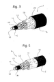
Figure 5 shows a further variant embodiment, similar in some
ways to that of Figure 3.
In the variant shown in Figure 5, the supporting wire 10 is
made from electrically insulating material (dielectric) and
can be, in particular, an optical fibre. On this supporting
wire 10 there is deposited a first layer 15 of electrically
conductive material, acting in operation as an anode (A).
Further layers 13, 12, 11 and 14 are deposited in succession
on top of the anode 15 as in the variant shown in Figure 2.
The outermost conductive layer 14 acts in operation as a
cathode C, and can be continuous or percolated, and nonhomogeneous
if necessary, and can be thin enough to be
substantially transparent to the generated radiation.
In a variant which is not shown, but which has essentially
the same structure as that shown in Figure 5, the internal
electrode 15 acting as the anode A is at least partially
transparent to the generated radiation, and is deposited on a
supporting wire 10 which is transparent to the emitted
radiation (optical fibre). Additionally, the external
electrode 14, acting as the cathode C, is reflective with
respect to the radiation. In this variant, the generated
radiation can be propagated along the optical fibre 10 acting
as the supporting wire for the electro-optical device, in a
way similar to that described in relation to Figures 3 and 4.
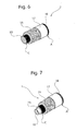
Figures 6 and 7 show two electro-optical devices 1 whose
stratified structure is such that it forms a crystalline
inorganic semiconductor LED.
The LED 1 of Figure 6 comprises a supporting wire 10, of
electrically conductive material, acting in operation as a
cathode. A coaxial cylindrical annular layer 16 of
semiconductor material, for example Gan, InGan, AlInGaP,
etc., with n-type doping, is deposited on the conductive
supporting wire 10. On this layer there is deposited a
further layer 17 of semiconductor material, of a type similar
to that of the layer 16, but with p-type doping. An outermost
electrically conductive layer 18, acting in operation as an
anode (A), is deposited on the layer 17.
A layer of crystalline intrinsic semiconductor, allowing the
epitaxial growth of the crystalline layers forming the
junction, can be deposited between the supporting wire 10 and
the n-type layer 16. The said intrinsic semiconductor can be
the same material as that used for the p and/or n layer, or a
different material which is crystallographically compatible
with the layers forming the junction.
In operation, when a forward biasing voltage is applied
between the anode and cathode, the recombination of the
electrons and holes in the depletion layer of the p-n
junction causes energy to be emitted in the form of
radiation.
The external electrode 18 acting as the anode A can be made
with apertures to allow the exit of the radiation, or can be
made thin enough to be at least partially transparent to the
generated radiation.
In an advantageous configuration, the thicknesses between the
active layers are such that a microcavity resonant at the
emission wavelength is formed.
In a variant embodiment which is not shown, the inorganic LED
device according to the invention consists of a multilevel
heterostructure, at levels positioned according to layers
deposited on a cylindrical substrate.
In a further variant which is not shown, the supporting wire
10 of electrically conductive material acts as the anode, and
the outermost conductive layer acts in operation as the
cathode.
In the variant shown in Figure 7, the same reference symbols
are given to parts and elements described previously.
In the embodiment shown in Figure 7, the supporting wire 10
of the electro-optical diode device 1 is made from
electrically insulating material (dielectric), such as an
optical fibre. An electrically conductive layer 15, which may
for example be metallic, is deposited on this wire and acts
in operation as the cathode C. The layers 16, 17 and 18 are
then deposited on the internal electrode 15, as in the device
shown in Figure 6.
In a variant which is not shown, the internal electrode of
the electro-optical device 1 shown in Figure 7 is at least
partially transparent to the generated radiation, and the
supporting wire 10 of dielectric material is optically
transparent (optical fibre). In this case, the generated
radiation is propagated along the supporting wire 10.
In variant embodiments which are not shown, but are
structurally similar to those shown in Figures 6 and 7,
electro-optical diode devices according to the invention can
act as photodiodes or as photovoltaic converters.
Figures 8 and 9 are schematic illustrations of inorganic
electro-optical devices according to the invention, of the
TFEL or TDEL type.
The device 1 of Figure 8 comprises an optically transparent
supporting wire 10 (optical fibre) on which are deposited in
succession a transparent conductive layer 15 acting as an
electrode, an insulating layer 116, a layer of luminescent
semiconductor material 117, a further insulating layer 118
and an external conductive layer 18 acting as an electrode.
The considerations expressed previously in relation to
Figures 3 and 4 are applicable, mutatis mutandis, to the
electro-optical device 1 of Figure 8.
The device 1 of Figure 9 has a structure similar to that of
the device shown in Figure 8, formed on a non-transparent
supporting wire 10. The layer 15 acting as an internal
electrode is also non-transparent, while the external
electrode 18 is at least partially transparent.
Figures 10 and 11 are schematic and partial illustrations of
electro-optical diode devices according to the invention in
which the outermost electrode is substantially reflective
with respect to the radiation generated in operation. These
electro-optical devices incorporate optical devices allowing
the emitted radiation to be extracted in the outward radial
direction.
Figure 10 is a schematic representation of the structure of
an electro-optical LED device, whose structure is essentially
of the type described with reference to Figure 6.
The stratified structure 16-18 of the electro-optical device
1 of Figure 10 has a plurality of breaks 20, in each of which
is positioned an annular reflector device 21 for diverting
the generated radiation in an outward radial direction. In
the illustrated embodiment, each reflector device 21
comprises an annular prism 22 with a triangular section, with
the apical circumference facing outwards, having a first
refractive index n1, incorporated in an at least partially
transparent ring 23, having a second refractive index n2.
Figure 11 shows two different solutions for enabling the
radiation to be extracted in an electro-optical device 1. In
the solution shown in the upper part of Figure 11, a
corrugation 25, capable of substantially diffusing the
incident radiation radially outwards, is formed at the
interface between the internal electrode (cathode or anode
10) and the innermost semiconductor layer 16. This
corrugation 25 extends along the internal electrode 10 at the
position of a discontinuity or aperture 26 of the external
electrode 18, through which the radiation can emerge
radially.
The lower part of Figure 11 shows a variant embodiment in
which a transparent element 29, provided with a corrugation
30 capable of substantially diffusing the generated radiation
radially outwards, is positioned in a discontinuity or
aperture 27 of the external electrode 18.
The scope of the present invention also includes any
radiation emitting apparatus comprising a plurality of
electro-optical emitters of the types described above.
The scope of the invention also includes any radiation
emitting apparatus which comprises at least one photoemitter
device of one of the types described above, and at least one
photodiode device as described above, used as an electrical
generator for a power supply.
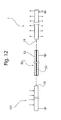
Figure 12 shows, by way of example and schematically, an
arrangement in which a photoemitter device 1 according to the
invention is coupled to a photodiode 101 according to the
invention acting as an electrical generator, with the
interposition of an electrical energy accumulator device 50.
This accumulator device can comprise, for example, a
capacitor, with an inner plate 51, in the form of a rigid or
flexible wire for example, and an associated coaxial outer
plate 52, with the interposition of a dielectric. This
coaxial cylindrical configuration of the accumulator enables
it to be integrated with the photodiode 101 or with the
photoemitter device 1 if required.
Figure 13 shows, in a schematic and simplified way, a
solution which, on an optical fibre 10, uses a device 1A
according to the invention, acting as a means of detecting an
optical signal a emitted by a remote emitter and propagated
along the fibre 10, and another device 1B according to the
invention, acting as a means of emission. These devices 1A
and 1B are connected electrically to an electronic system ES
capable of amplifying the detected signal b obtained by the
conversion of the corresponding optical signal a, and of
supplying the amplified electronic signal c to the emitter
device 1B to cause an amplified optical signal A to be
propagated in the fibre.
Electro-optical diode devices according to the invention can
be made in the form of flexible wire-like emitters, having
dimensions so small that they can be interwoven to form an
illuminable textile, having entirely distinctive aesthetic
effects.
Clearly, provided that the principle of the invention is
retained, the forms of embodiment and the details of
construction can be varied widely from what has been
described and illustrated purely by way of example and
without restrictive intent, without departure from the scope
of the invention as defined in the attached claims.