EP1569270A2 - Manufacturing method of semiconductor device - Google Patents
Manufacturing method of semiconductor device Download PDFInfo
- Publication number
- EP1569270A2 EP1569270A2 EP05004336A EP05004336A EP1569270A2 EP 1569270 A2 EP1569270 A2 EP 1569270A2 EP 05004336 A EP05004336 A EP 05004336A EP 05004336 A EP05004336 A EP 05004336A EP 1569270 A2 EP1569270 A2 EP 1569270A2
- Authority
- EP
- European Patent Office
- Prior art keywords
- semiconductor
- forming
- semiconductor chip
- semiconductor device
- respect
- Prior art date
- Legal status (The legal status is an assumption and is not a legal conclusion. Google has not performed a legal analysis and makes no representation as to the accuracy of the status listed.)
- Withdrawn
Links
Images






Classifications
-
- H—ELECTRICITY
- H10—SEMICONDUCTOR DEVICES; ELECTRIC SOLID-STATE DEVICES NOT OTHERWISE PROVIDED FOR
- H10P—GENERIC PROCESSES OR APPARATUS FOR THE MANUFACTURE OR TREATMENT OF DEVICES COVERED BY CLASS H10
- H10P74/00—Testing or measuring during manufacture or treatment of wafers, substrates or devices
- H10P74/23—Testing or measuring during manufacture or treatment of wafers, substrates or devices characterised by multiple measurements, corrections, marking or sorting processes
- H10P74/232—Testing or measuring during manufacture or treatment of wafers, substrates or devices characterised by multiple measurements, corrections, marking or sorting processes comprising connection or disconnection of parts of a device in response to a measurement
-
- A—HUMAN NECESSITIES
- A01—AGRICULTURE; FORESTRY; ANIMAL HUSBANDRY; HUNTING; TRAPPING; FISHING
- A01G—HORTICULTURE; CULTIVATION OF VEGETABLES, FLOWERS, RICE, FRUIT, VINES, HOPS OR SEAWEED; FORESTRY; WATERING
- A01G31/00—Soilless cultivation, e.g. hydroponics
- A01G31/02—Special apparatus therefor
-
- A—HUMAN NECESSITIES
- A01—AGRICULTURE; FORESTRY; ANIMAL HUSBANDRY; HUNTING; TRAPPING; FISHING
- A01G—HORTICULTURE; CULTIVATION OF VEGETABLES, FLOWERS, RICE, FRUIT, VINES, HOPS OR SEAWEED; FORESTRY; WATERING
- A01G9/00—Cultivation in receptacles, forcing-frames or greenhouses; Edging for beds, lawn or the like
- A01G9/02—Receptacles, e.g. flower-pots or boxes; Glasses for cultivating flowers
-
- H—ELECTRICITY
- H10—SEMICONDUCTOR DEVICES; ELECTRIC SOLID-STATE DEVICES NOT OTHERWISE PROVIDED FOR
- H10W—GENERIC PACKAGES, INTERCONNECTIONS, CONNECTORS OR OTHER CONSTRUCTIONAL DETAILS OF DEVICES COVERED BY CLASS H10
- H10W70/00—Package substrates; Interposers; Redistribution layers [RDL]
- H10W70/01—Manufacture or treatment
- H10W70/05—Manufacture or treatment of insulating or insulated package substrates, or of interposers, or of redistribution layers
-
- H—ELECTRICITY
- H10—SEMICONDUCTOR DEVICES; ELECTRIC SOLID-STATE DEVICES NOT OTHERWISE PROVIDED FOR
- H10W—GENERIC PACKAGES, INTERCONNECTIONS, CONNECTORS OR OTHER CONSTRUCTIONAL DETAILS OF DEVICES COVERED BY CLASS H10
- H10W70/00—Package substrates; Interposers; Redistribution layers [RDL]
- H10W70/60—Insulating or insulated package substrates; Interposers; Redistribution layers
- H10W70/62—Insulating or insulated package substrates; Interposers; Redistribution layers characterised by their interconnections
- H10W70/65—Shapes or dispositions of interconnections
- H10W70/654—Top-view layouts
- H10W70/656—Fan-in layouts
-
- H—ELECTRICITY
- H10—SEMICONDUCTOR DEVICES; ELECTRIC SOLID-STATE DEVICES NOT OTHERWISE PROVIDED FOR
- H10W—GENERIC PACKAGES, INTERCONNECTIONS, CONNECTORS OR OTHER CONSTRUCTIONAL DETAILS OF DEVICES COVERED BY CLASS H10
- H10W72/00—Interconnections or connectors in packages
- H10W72/01—Manufacture or treatment
- H10W72/012—Manufacture or treatment of bump connectors, dummy bumps or thermal bumps
-
- H—ELECTRICITY
- H10—SEMICONDUCTOR DEVICES; ELECTRIC SOLID-STATE DEVICES NOT OTHERWISE PROVIDED FOR
- H10W—GENERIC PACKAGES, INTERCONNECTIONS, CONNECTORS OR OTHER CONSTRUCTIONAL DETAILS OF DEVICES COVERED BY CLASS H10
- H10W72/00—Interconnections or connectors in packages
- H10W72/01—Manufacture or treatment
- H10W72/019—Manufacture or treatment of bond pads
-
- H—ELECTRICITY
- H10—SEMICONDUCTOR DEVICES; ELECTRIC SOLID-STATE DEVICES NOT OTHERWISE PROVIDED FOR
- H10W—GENERIC PACKAGES, INTERCONNECTIONS, CONNECTORS OR OTHER CONSTRUCTIONAL DETAILS OF DEVICES COVERED BY CLASS H10
- H10W72/00—Interconnections or connectors in packages
- H10W72/20—Bump connectors, e.g. solder bumps or copper pillars; Dummy bumps; Thermal bumps
- H10W72/241—Dispositions, e.g. layouts
- H10W72/244—Dispositions, e.g. layouts relative to underlying supporting features, e.g. bond pads, RDLs or vias
-
- H—ELECTRICITY
- H10—SEMICONDUCTOR DEVICES; ELECTRIC SOLID-STATE DEVICES NOT OTHERWISE PROVIDED FOR
- H10W—GENERIC PACKAGES, INTERCONNECTIONS, CONNECTORS OR OTHER CONSTRUCTIONAL DETAILS OF DEVICES COVERED BY CLASS H10
- H10W72/00—Interconnections or connectors in packages
- H10W72/20—Bump connectors, e.g. solder bumps or copper pillars; Dummy bumps; Thermal bumps
- H10W72/251—Materials
- H10W72/252—Materials comprising solid metals or solid metalloids, e.g. PbSn, Ag or Cu
-
- H—ELECTRICITY
- H10—SEMICONDUCTOR DEVICES; ELECTRIC SOLID-STATE DEVICES NOT OTHERWISE PROVIDED FOR
- H10W—GENERIC PACKAGES, INTERCONNECTIONS, CONNECTORS OR OTHER CONSTRUCTIONAL DETAILS OF DEVICES COVERED BY CLASS H10
- H10W72/00—Interconnections or connectors in packages
- H10W72/90—Bond pads, in general
- H10W72/921—Structures or relative sizes of bond pads
- H10W72/922—Bond pads being integral with underlying chip-level interconnections
-
- H—ELECTRICITY
- H10—SEMICONDUCTOR DEVICES; ELECTRIC SOLID-STATE DEVICES NOT OTHERWISE PROVIDED FOR
- H10W—GENERIC PACKAGES, INTERCONNECTIONS, CONNECTORS OR OTHER CONSTRUCTIONAL DETAILS OF DEVICES COVERED BY CLASS H10
- H10W72/00—Interconnections or connectors in packages
- H10W72/90—Bond pads, in general
- H10W72/921—Structures or relative sizes of bond pads
- H10W72/922—Bond pads being integral with underlying chip-level interconnections
- H10W72/9223—Bond pads being integral with underlying chip-level interconnections with redistribution layers [RDL]
-
- H—ELECTRICITY
- H10—SEMICONDUCTOR DEVICES; ELECTRIC SOLID-STATE DEVICES NOT OTHERWISE PROVIDED FOR
- H10W—GENERIC PACKAGES, INTERCONNECTIONS, CONNECTORS OR OTHER CONSTRUCTIONAL DETAILS OF DEVICES COVERED BY CLASS H10
- H10W72/00—Interconnections or connectors in packages
- H10W72/90—Bond pads, in general
- H10W72/921—Structures or relative sizes of bond pads
- H10W72/923—Bond pads having multiple stacked layers
-
- H—ELECTRICITY
- H10—SEMICONDUCTOR DEVICES; ELECTRIC SOLID-STATE DEVICES NOT OTHERWISE PROVIDED FOR
- H10W—GENERIC PACKAGES, INTERCONNECTIONS, CONNECTORS OR OTHER CONSTRUCTIONAL DETAILS OF DEVICES COVERED BY CLASS H10
- H10W72/00—Interconnections or connectors in packages
- H10W72/90—Bond pads, in general
- H10W72/941—Dispositions of bond pads
- H10W72/9415—Dispositions of bond pads relative to the surface, e.g. recessed, protruding
-
- H—ELECTRICITY
- H10—SEMICONDUCTOR DEVICES; ELECTRIC SOLID-STATE DEVICES NOT OTHERWISE PROVIDED FOR
- H10W—GENERIC PACKAGES, INTERCONNECTIONS, CONNECTORS OR OTHER CONSTRUCTIONAL DETAILS OF DEVICES COVERED BY CLASS H10
- H10W72/00—Interconnections or connectors in packages
- H10W72/90—Bond pads, in general
- H10W72/941—Dispositions of bond pads
- H10W72/942—Dispositions of bond pads relative to underlying supporting features, e.g. bond pads, RDLs or vias
-
- H—ELECTRICITY
- H10—SEMICONDUCTOR DEVICES; ELECTRIC SOLID-STATE DEVICES NOT OTHERWISE PROVIDED FOR
- H10W—GENERIC PACKAGES, INTERCONNECTIONS, CONNECTORS OR OTHER CONSTRUCTIONAL DETAILS OF DEVICES COVERED BY CLASS H10
- H10W72/00—Interconnections or connectors in packages
- H10W72/90—Bond pads, in general
- H10W72/951—Materials of bond pads
- H10W72/952—Materials of bond pads comprising metals or metalloids, e.g. PbSn, Ag or Cu
-
- Y—GENERAL TAGGING OF NEW TECHNOLOGICAL DEVELOPMENTS; GENERAL TAGGING OF CROSS-SECTIONAL TECHNOLOGIES SPANNING OVER SEVERAL SECTIONS OF THE IPC; TECHNICAL SUBJECTS COVERED BY FORMER USPC CROSS-REFERENCE ART COLLECTIONS [XRACs] AND DIGESTS
- Y02—TECHNOLOGIES OR APPLICATIONS FOR MITIGATION OR ADAPTATION AGAINST CLIMATE CHANGE
- Y02P—CLIMATE CHANGE MITIGATION TECHNOLOGIES IN THE PRODUCTION OR PROCESSING OF GOODS
- Y02P60/00—Technologies relating to agriculture, livestock or agroalimentary industries
- Y02P60/20—Reduction of greenhouse gas [GHG] emissions in agriculture, e.g. CO2
- Y02P60/21—Dinitrogen oxide [N2O], e.g. using aquaponics, hydroponics or efficiency measures
Definitions
- the present invention relates to a manufacturing method of a semiconductor device, and more specifically to a manufacturing method of a semiconductor device by processing of a wafer level.
- a method for manufacturing a semiconductor device by processing of a wafer level has been performed as a method for manufacturing a semiconductor device of a chip size package etc.
- a method for manufacturing a chip size package using processing of a wafer level there is a following manufacturing method of a semiconductor device of a chip size. That is, in a semiconductor wafer, a rewiring pattern is formed so that it is electrically connected to electrode terminals of individual semiconductor chips formed in the semiconductor wafer, and an external connection terminal is formed so that it is electrically connected to the rewiring pattern. Then a surface in which the external connection terminal of the semiconductor wafer is formed is sealed by resin, and the semiconductor wafer is cut into individual segments together with the resin after the sealing (for example, see JP-A-10-79362 and JP-A-8-330313).
- a plurality of semiconductor devices with the same structure are formed on the semiconductor wafer in arrangement aligned in length and width. These semiconductor devices are mounted on a substrate etc. respectively, after being cut into individual segments. Before the semiconductor devices are mounted on the substrate etc., conformity and nonconformity of electrical characteristics etc. of the respective semiconductor devices are judged by inspection and only conforming semiconductor devices are mounted on the substrate etc. Incidentally, inspection for judgment of conformity and nonconformity of a product is actually made at each stage of a manufacturing process of the semiconductor device. For example, at a stage of manufacturing the semiconductor wafer, inspection of conformity and nonconformity of electrical characteristics etc. of individual semiconductor chips formed in the semiconductor wafer is also made (for example, see JP-A-2004-31463).
- product inspection is made at each of the manufacturing stages in the manufacturing process of the semiconductor device. For example, at a stage of manufacturing the semiconductor wafer, characteristics of individual semiconductor chips are also tested.
- rewiring patterns or external connection terminals are formed with respect to all the semiconductor chips. That is, the rewiring patterns or external connection terminals are formed with respect to semiconductor chips judged as conforming product and also with respect to semiconductor chips judged as nonconforming product. This is because in the manufacturing process, it is difficult not to form the rewiring pattern etc. on only the semiconductor chips judged as nonconforming product.
- a resist pattern for forming the rewiring pattern is formed by a photolithographic process using an exposure mask. Therefore, in order to perform exposure so as not to form the resist pattern on the nonconforming semiconductor chips, a mask with special shape in which an unexposed portion is provided in accordance with a position of the nonconforming semiconductor chips must be prepared. Since occurrence positions of the nonconforming semiconductor chips vary depending on the respective semiconductor wafers, it is actually impossible to prepare such a mask with special shape.
- the rewiring patterns etc. are formed to manufacture the semiconductor device at a wafer level regardless of the inspection result of the semiconductor chips at the manufacturing stage of the semiconductor wafer. Therefore, there were problems that in the case of inspecting a formed semiconductor device, accurate inspection cannot be made or an inspection apparatus is damaged or adverse influence on other conforming semiconductor device is had.
- An obj ect of the present invention is to provide a manufacturing method of a semiconductor device capable of making accurate inspection without damaging an inspection apparatus or having adverse influence on a conforming semiconductor device in the case of inspecting electrical characteristics etc. with respect to a manufactured semiconductor device, in a process of manufacturing the semiconductor device by processing of a wafer level.
- the present invention comprises the following configurations in order to achieve the object.
- a method for manufacturing a semiconductor device by processing of a wafer level comprises: in the case of forming the semiconductor device at the wafer level, performing a treatment for forming a circuit including a rewiring pattern with respect to a semiconductor chip judged as a conforming product on the basis of inspection results on individual semiconductor chips constituting a semiconductor wafer; and performing a treatment for avoiding having adverse influence on a semiconductor device of a conforming product or an inspection apparatus in an inspection of a formed semiconductor device after forming the semiconductor device with respect to a semiconductor chip judged as a nonconforming product on the basis of the inspection results on induvidual semiconductor chips.
- this is achieved by not forming a rewiring pattern.
- the treatment for avoiding having adverse influence on the semiconductor device of the conforming product or the inspection apparatus in the inspection of the formed semiconductor device after forming the semiconductor device with respect to the semiconductor chip judged as the nonconforming product may be a treatment in which the semiconductor chip is electrically disconnected from a circuit electrically connected to an electrode pad of the semiconductor chip.
- the circuit electrically connected to the electrode pad of the semiconductor chip preferably includes a rewiring pattern connected to the electrode pad, and an external connection terminal etc. formed by joining a solder ball or by plating.
- a rewiring pattern for electrically connecting an electrode pad to an external connection terminal may be formed with respect to the semiconductor chip judged as the conforming product, and, the rewiring pattern may not be formed with respect to the semiconductor chip judged as the nonconforming product and it is formed in a state of electrically disconnecting the electrode pad from the external connection terminal.
- the semiconductor chip judged as the nonconforming product is electrically disconnected from the external connection terminal, and in the case of inspecting the semiconductor device in a post-process, the semiconductor chip judged as the nonconforming product does not have adverse influence on an inspection apparatus etc. and accurate inspection etc. can be made.
- a method in which with respect to the semiconductor chip judged as the nonconforming product, the rewiring pattern is not formed and the electrode pad is electrically disconnected from the external connection terminal may be a method in which an undercoat metal layer is formed on an electrode terminal formation surface of the semiconductor wafer and a resist pattern to which a region for forming the rewiring pattern electrically connected to the electrode pad of the semiconductor chip is exposed is formed on a surface of the undercoat metal layer and then, with respect to the semiconductor chip judged as the nonconforming product, a resist is applied to the region for forming the rewiring pattern and the region for forming the rewiring pattern is coated with the resist and then, a plating using the undercoat metal layer as a plating feeding layer is performed with respect to the semiconductor wafer and a conductor layer resulting in the rewiring pattern is formed in only the semiconductor chip judged as the conforming product.
- a method in which with respect to the semiconductor chip judged as the nonconforming product, the rewiring pattern is not formed and the electrode pad is electrically disconnected from the external connection terminal may be a method in which an undercoat metal layer is formed on an electrode terminal formation surface of the semiconductor wafer, and a resist pattern, to which a region for forming the rewiring pattern electrically connected to the electrode pad of the semiconductor chip is exposed and which coats the region for forming the rewiring pattern with respect to the semiconductor chip judged as the nonconforming product, is formed on a surface of the undercoat metal layer, and then, a plating using the undercoat metal layer as a plating feeding layer is performed with respect to the semiconductor wafer and a conductor layer resulting in the rewiring pattern is formed in only the semiconductor chip judged as the conforming product.
- a manufacturing method of a semiconductor device in accordance with the present invention in the case of forming the semiconductor device by processing of a wafer level, with respect to a semiconductor chip judged as a nonconforming product on the basis of inspection results in a semiconductor wafer, a treatment without having adverse influence on a semiconductor device of a conforming product or damaging an inspection apparatus in the case of burn-in or inspection in a post-process is performed, independently of a semiconductor chip judged as a conforming product. Therefore, the damage etc. to the inspection apparatus can be avoided to make accurate inspection etc.
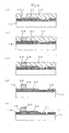
- Figs. 1 to 3 show a process example for forming a semiconductor device by a processing method of a wafer level.
- Fig. 1(a) shows a configuration of an electrode terminal formation surface of a semiconductor wafer 10 in which an electrode pad 14 is formed, and shows a state in which a surface of the semiconductor wafer 10 is coated with a passivation film 12 and the electrode pad 14 of aluminum is exposed from the passivation film 12.
- Fig. 1(b) shows a state in which an insulating layer 16 is formed on a surface of the passivation film 12.
- the insulating layer 16 can be formed by coating the surface of the passivation film 12 with an insulating material such as a polyimide film and exposing the electrode pad 14.
- Fig. 1(c) shows a state in which surfaces of the electrode pad 14 and the insulating layer 16 are coated with an undercoat metal layer 18.
- the undercoat metal layer 18 is formed, for example, by sputtering chromium and then sputtering copper.
- Fig. 1(d) shows a state in which a resist pattern 20 for forming a rewiring pattern is formed on a surface of the undercoat metal layer 18 by a predetermined pattern.
- Fig. 1(e) is a state in which copper plating is performed using the undercoat metal layer 18 as a plating feeding layer and a conductor layer resulting in a rewiring pattern 22 is formed on an exposed portion of the undercoat metal layer 18.
- Fig. 1(f) shows a state in which the resist pattern 20 is removed. The rewiring pattern 22 is formed in a state of being electrically connected to the electrode pad 14.
- Fig. 2 shows a process of forming an external connection terminal on the rewiring pattern 22.
- Fig. 2 (a) shows a state in which a resist pattern 24 is formed so as to expose a region for forming an external connection terminal on the rewiring pattern 22 in order to form the external connection terminal by plating.
- Numeral 24a is an exposure hole in which the rewiring pattern 22 is exposed from the resist pattern 24.
- Fig. 2 (b) shows a state in which copper plating is performed using the undercoat metal layer 18 as a plating feeding layer and the copper plating is heaped up in the exposure hole 24a and a copper post 26 is formed.
- Fig. 2(c) shows a state in which a barrier metal layer 28 is covered and formed on an exposure end face of the top of the copper post 26.
- the barrier metal layer 28 can be formed, for example, by performing nickel plating and gold plating in this order.
- Fig. 2 (d) shows a state in which the resist pattern 24 is removed.
- an external connection terminal 30 is exposed to the outside, and the undercoat metal layer 18 and the rewiring pattern 22 formed on a surface of the undercoat metal layer 18 are exposed to a surface of the semiconductor wafer 10.
- Fig. 2(e) is a state in which an exposure portion of the undercoat metal layer 18 is etched and the insulating layer 16 is exposed to a surface of the semiconductor wafer 10, and the rewiring pattern 22 is formed on a surface of the insulating layer 16 in a predetermined independent pattern.
- a region coated with the rewiring pattern 22 in the undercoat metal layer 18 is left on the insulating layer 16, and the rewiring pattern 22 is electrically connected to the electrode pad 14 and the external connection terminal 30 is electrically connected to the electrode pad 14 through the rewiring pattern 22.
- Fig. 3 shows a process of sealing an electrode terminal formation surface of the semiconductor wafer 10 in which the external connection terminal 30 described above is formed by resin.
- Fig. 3(a) shows a state in which the semiconductor wafer 10 in which the external connection terminal 30 is formed is set in the side of a lower mold of a resin sealing apparatus.
- Numeral 40 is an upper mold
- numeral 41 is an inside lower mold
- numeral 42 is an outside lower mold.
- Numeral 43 is a temporary film for coating a molding surface of the upper mold 40.
- the semiconductor wafer 10 is arranged in a state in which a surface in which the external connection terminal 30 is formed is directed toward the upper mold 40, and a resin tablet 44 is supplied on the semiconductor wafer 10.
- Fig. 3 (b) shows a state in which clamping of the semiconductor wafer 10 is started by a metal mold. After the outer periphery of the semiconductor wafer 10 is closed by the upper mold 40 and the outside lower mold 42, the semiconductor wafer 10 together with the resin tablet 44 are clamped by the inside lower mold 41 and the upper mold 40, and resin 44a melted by heating is gradually charged into a cavity 45.
- Fig. 3(c) shows a state in which the metal mold is clamped to a mold clamping position and the resin 44a is fully charged into the whole cavity 45 and the semiconductor wafer 10 is compressed and molded.
- Fig. 3 (d) shows a state in which the mold is opened after the resin 44a hardens.
- the surface of the semiconductor wafer 10 in which the external connection terminal 30 is formed is fully sealed by the resin 44a.
- an end face of the external connection terminal 30 is exposed to a surface of the resin 44a.
- the temporary film 43 is peeled and a solder ball 46 is joined to the end face of the external connection terminal 30. Thereafter, semiconductor device of individual segments canbe obtained by cutting the semiconductor wafer 10 together with the resin 44a every area of semiconductor chips.
- Fig. 4(a) shows a state of joining the solder ball 46 to the end face of the external connection terminal 30 and a configuration of a semiconductor device 50 (chip size package) in which the semiconductor wafer 10 is cut into individual segments.
- Numeral 10a is a semiconductor chip cut into individual segments.
- Fig. 4(b) enlarges and shows a state in which the surface of the semiconductor device 50 in which the external connection terminal 30 is formed is sealed by the resin 44a and the solder ball 46 and the external connection terminal 30 are electrically connected to the electrode pad 14 of the semiconductor chip through the rewiring pattern 22.
- the manufacturing method of the semiconductor device described above shows an example of a manufacturing process of manufacturing the semiconductor device by processing of a wafer level.
- a manufacturing method of a semiconductor device according to the present invention is characterized in that in the case of performing a treatment for forming the rewiring pattern 22 or forming the external connection terminal 30 at the wafer level as described above, on the basis of results in which individual semiconductor chips are inspected at a stage of manufacturing the semiconductor wafer 10, a treatment different from treatment with respect to a semiconductor chip judged as a conforming product described above is performed with respect to a semiconductor chip judged as a nonconforming product.
- the rewiring pattern 22 is formed or a plating treatment is performed in like manner with respect to all the semiconductor chips of the semiconductor wafer.
- a treatment different from that of a semiconductor chip of a conforming product is performed so as not to damage an inspection apparatus or have adverse influence on a semiconductor device of a conforming product in the case of a treatment such as burn-in or an inspection after forming the semiconductor device by forming the rewiring pattern 22 or the external connection terminal 30 and performing sealing by resin.
- the treatment different from treatment with respect to a semiconductor chip of a conforming product refers to a treatment performed so as not to damage an inspection apparatus in the case of an inspection after forming a semiconductor device or have adverse influence on a semiconductor device of a conforming product in the case of burn-in.
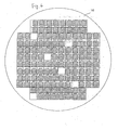
- Fig. 5 shows a result (wafer electrical nonconformity map) of judging conformity and nonconformity of semiconductor chips by testing electrical characteristics etc. of individual semiconductor chips at a manufacturing stage of a semiconductor wafer.
- Fig. 5 shows the semiconductor chips in which division portions described as F are judged as nonconformity.
- Fig. 6 explanatorily shows a state of forming rewiring patterns on an electrode terminal formation surface of the semiconductor wafer 10.
- Fig. 6 shows that the rewiring patterns are not formed in regions of the semiconductor chips judged as nonconformity in Fig. 5.
- external connection terminals are not shown with respect to the semiconductor chips judged as nonconformity in Fig. 6.
- an inspection apparatus or a burn-in apparatus is electrically disconnected from the semiconductor chips and the semiconductor chips of the nonconforming products do not have adverse influence on the inspection apparatus or the burn-in apparatus.
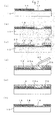
- Fig. 7 shows one exemplary, non-limiting example of a method constructed so that rewiring patterns 22 are not electrically connected to electrode pads 14 with respect to regions of semiconductor chips judged as nonconforming products in the case of forming the rewiring patterns 22 on the electrode terminal formation surface of the semiconductor wafer 10 shown in Figs. 1 to 4 described above.
- Fig. 7 (a) shows a state in which an insulating layer 16 is formed on a surface of a semiconductor wafer 10
- Fig. 7 (b) shows a state in which a surface of the semiconductor wafer 10 is coated with an undercoat metal layer 18
- Fig. 7(c) shows a state in which a resist pattern 20 is formed so as to expose a region for forming a rewiring pattern 22 on a surface of the undercoat metal layer 18.
- a resist 20a is dropped to a region to which the undercoat metal layer 18 is exposed so that the region to which the undercoat metal layer 18 is exposed is coated as shown in Fig. 7(d).
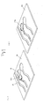
- Fig. 9 shows a state in which a resist pattern 20 is formed on a surface of an undercoat metal layer 18 by a perspective view.
- Fig. 9 (a) shows a state in which a resist 20a is dropped to a region to which the undercoat metal layer 18 is exposed in order to form a rewiring pattern 22, and
- Fig. 9 (b) shows a state in which the region to which the undercoat metal layer 18 is exposed is coated with the resist 20a. Since the region to which the undercoat metal layer 18 is exposed is formed in groove shape, the resist 20a flows along the groove and the resist 20a flows so as to bury the groove and the region of undercoat metal layer 18 is coated.
- Fig. 10 shows a state in which using a nozzle 60, a resist 20a is applied to regions of semiconductor chips judged as nonconforming products in a semiconductor wafer 10 based on results of inspecting individual semiconductor chips at a manufacturing stage of a semiconductor wafer. Since the inspection results of the semiconductor wafer are stored as map data, the semiconductor wafer 10 in which a resist pattern 20 is formed is sucked and supported on an X-Y stage 62 and based on the map data of the inspection results of the semiconductor wafer 10, the semiconductor chips of the nonconforming products are aligned with the nozzle 60 and the resist 20a is applied to surfaces of the semiconductor chips. Therefore, a treatment shown in Fig. 7(d) can be performed with respect to all the semiconductor chips judged as the nonconforming products in the semiconductor wafer 10.
- Fig. 7 (e) is a process of forming a conductor layer resulting in the rewiring pattern 22 on an exposed surface of the undercoat metal layer 18 using the undercoat metal layer 18 as a plating feeding layer.
- the undercoat metal layer 18 is coated with the resist 20a, so that the conductor layer is not formed on a surface of the undercoat metal layer 18.
- the rewiring pattern 22 is formed on the surface of the undercoat metal layer 18 with respect to a semiconductor chip judged as a conforming product as shown in Fig. 1(e).
- Fig. 7 (f) shows a state of removing the resist pattern 20 and the resist 20a.
- an external connection terminal 30 is formed in the same process as the process shown in Fig. 2.
- a process of forming the external connection terminal 30 is shown in Fig. 8.
- a resist pattern 24 is formed (Fig. 8 (a)) and a copper post 26 is formed by plating using the undercoat metal layer 18 as a plating feeding layer (Fig. 8 (b)) and the external connection terminal 30 is formed.
- the external connection terminal 30 is formed on the rewiring pattern 22 with respect to a semiconductor chip of a conforming product.
- the external connection terminal 30 is formed on the undercoat metal layer 18 without intervention of a conductor layer resulting in the rewiring pattern 22 with respect to a semiconductor chip of a nonconforming product (Fig. 8(c)).
- the undercoat metal layer 18 is etched and removed. Therefore, with respect to a region in which the semiconductor chip of the nonconforming product is formed, the undercoat metal layer 18 remains in only a region in which the external connection terminal 30 is formed so that the external connection terminal 30 is electrically disconnected from an electrode pad 14 (Fig. 8(d)).
- Formation of the external connection terminal 30 with respect to the semiconductor chip judged as the nonconforming product in the semiconductor wafer 10 thus has an advantage capable of forming the external connection terminal 30 made of the copper post 26 with normal shape.
- the external connection terminal 30 made of the copper post 26 is formed by electrolytic plating, a process is adjusted so that plating conditions (current density or plating deposition speed) on the semiconductor wafer become uniform in each of the regions (the center and periphery of the wafer) of the semiconductor wafer. Therefore, in the case of being constructed so that the copper post 26 is not formed on a nonconforming chip, the plating conditions in each of the regions on the semiconductor wafer become nonuniform and the copper post 2 6 with normal shape cannot be formed on a conforming chip.
- the copper post 26 is formed even when the rewiring pattern 22 is not formed, so that such a problem can be avoided.
- plating of the rewiring pattern is not performed on the nonconforming chip, so that the plating conditions on the semiconductor wafer become nonuniform strictly.
- a plating thickness (5 to 10 ⁇ m) of the rewiring pattern is very thin as compared with a height (about 100 ⁇ m) of the copper post, so that there is no problem actually.
- the external connection terminals 30 are formed on the nonconforming chips, so that the external connection terminals 30 are uniformly present on the semiconductor wafer.
- contact pressure of a contact probe of an inspection apparatus becomes uniform on the external connection terminals of each of the regions on the semiconductor wafer and connection between each of the external connection terminals and the contact probe can be made well and accurate inspection can be made.
- Fig. 11 shows an exemplary, non-limiting example of manufacture using a negative type resist as a method in which a rewiring pattern 22 is not formed with respect to a semiconductor chip judged as a nonconforming product.
- Fig. 11 (a) and 11 (b) are the same process as that of Fig. 7 (a) and 7 (b) and show a process of forming an insulating layer 16 on a surface of a semiconductor wafer 10 and further forming an undercoat metal layer 18.
- Fig. 11(c) shows a state in which a surface of the undercoat metal layer 18 is coated with a negative resist 20b in order to form the rewiring pattern 22.
- a region irradiated with light remains. Therefore, with respect to a semiconductor chip of a conforming product, it is constructed so as not to irradiate a region for forming the rewiring pattern 22 with light using a mask. On the other hand, with respect to a semiconductor chip of a nonconforming product, it is constructed so as to irradiate the region for forming the rewiring pattern 22 with focused light such as laser light as shown in Fig. 11 (d).
- Fig. 12 shows a state in which a position of a semiconductor chip judged as a nonconforming product is irradiated with light (ultraviolet light) in a spot manner in a state (state of Fig. 11(c)) of coating a surface of a semiconductor wafer 10 with the negative resist 20b based on inspection results at a manufacturing stage of the semiconductor wafer 10.
- the semiconductor chip judged as the nonconforming product can be irradiated with the light from a light source 64 by positioning and moving the semiconductor wafer 10 by an X-Y stage 62 based on map data of the inspection results of the semiconductor wafer 10.
- the rewiring pattern 22 is not formed with respect to the semiconductor chip judged as the nonconforming product and in a manner completely similar to the process shown in Figs. 7 and 8, the semiconductor chip judged as the nonconforming product can be rendered a state in which an electrode pad 14 is electrically disconnected from an external connection terminal 30.
- Fig. 13 shows a state of performing burn-in after a surface on which an external connection terminal 30 of a semiconductor wafer 10 is formed is sealed by resin 44a.
- Numeral 70 is a support chuck of the semiconductor wafer 10
- numeral 72 is a contactor
- numerals 74 are contact bumps (contact probes).
- the semiconductor wafer 10 after resin sealing is clamped by the support chuck 70 and the contactor 72 and is heated inside an oven and also the contact bumps 74 are pressed and contacted to the external connection terminals 30 of respective semiconductor device and a voltage higher than a normal working voltage is applied.
- numeral 50 is a semiconductor device in which a semiconductor chip 10a is judged as a conforming product and numeral 51 is a semiconductor device in which a semiconductor chip 10b is judged as a nonconforming product. It is shown that an electrode pad 14 is electrically connected to the external connection terminal 30 through a rewiring pattern 22 in the semiconductor device 50 made of the semiconductor chip 10a of the conforming product. Also, it is shown that the electrode pad 14 is electrically disconnected from the external connection terminal 30 in the semiconductor device 51 made of the semiconductor chip 10b of the nonconforming product. As described above, by forming the external connection terminal 30 with respect to the semiconductor chip judged as the nonconforming product in a manner similar to the conforming product, the semiconductor wafer 10 can surely be clamped by the support chuck 70 and the contactor 72.
- the semiconductor chip 10b is electrically disconnected from the external connection terminal 30 with respect to the semiconductor device 51 made of the semiconductor chip 10b judged as the nonconforming product. Therefore, the contactor 72 is electrically separated from the semiconductor chip 10b judged as the nonconforming product and an overcurrent can be prevented from flowing in the semiconductor chip 10b. Therefore, a burn-in apparatus is not damaged and adverse influence on the semiconductor chip 10a of the conforming product in the vicinity due to overheating of the semiconductor chip of the nonconforming product can be prevented.
- a method for manufacturing a semiconductor device by processing of a wafer level is not limited to the manufacturing method described above, and can also be achieved by other methods, and a form of a chip size package also includes several kinds.
- the undercoat metal layer 18 is formed and the conductor layer resulting in the rewiring pattern 22 is formed and then the copper post 26 resulting in the external connection terminal 30 is formed by copper plating.
- the copper post 26 instead of forming the copper post 26, there is also a method for forming an external connection terminal by merely joining a solder ball to a rewiring pattern 22. Its manufacturing method is shown in Fig. 14.
- Fig. 14(a) shows a state in which a rewiring pattern 22 is formed on a surface of a semiconductor wafer 10 in a manner similar to the method shown in Figs. 1 (a) to 1 (f).
- Fig. 14 (b) shows a state in which a polyimide film etc. are laminated on the surface of the semiconductor wafer 10 to form an insulating film 32 and a pad 22a for joining a solder ball is exposed.
- Fig. 14 (c) is a state of forming an external connection terminal by joining a solder ball 34 to the pad 22a.
- a region for forming the rewiring pattern is not exposed to the undercoat metal layer 18 so as not to form the rewiring pattern and thereby the rewiring pattern is not formed and the solder ball 34 is not joined and it can be rendered a state in which the solder ball and an electrode pad 14 are electrically disconnected from the outside.
- FIG. 14 (d) shows a situation in which with respect to a region in which a nonconforming semiconductor chip is formed, a metal layer such as the rewiring pattern is not formed and the insulating layer 16 is exposed. Therefore, the solder ball is not joined to an opening 32a of the insulating film 32 after forming the insulating film 32 (Fig. 14(e)).
- the embodiment described above shows the example of avoiding a situation in which an inspection apparatus etc. in a post-process are directly electrically connected to a semiconductor chip judged as a nonconforming product by previous inspection by means of a method applicable in a related-art manufacturing process of a semiconductor device of a wafer level.
- a method for electrically disconnecting the semiconductor chip of the nonconforming product from the inspection apparatus etc. is not limited to the method of the embodiment described above.
- a method for forming a dummy external connection terminal with the same form as that of an external connection terminal 30 by burying a resin material made of an electrical insulator in an exposure hole 24a so that a copper post 26 is not formed with respect to a semiconductor chip of a nonconforming product in the case of forming the external connection terminal 30 can also be used.
- a rewiring pattern 22 may be formed also with respect to the semiconductor chip of the nonconforming product.
Landscapes
- Life Sciences & Earth Sciences (AREA)
- Environmental Sciences (AREA)
- Testing Or Measuring Of Semiconductors Or The Like (AREA)
- Internal Circuitry In Semiconductor Integrated Circuit Devices (AREA)
Abstract
Description
- This application claims foreign priority based on Japanese patent application JP 2004-050652, filed on February 26, 2004, the contents of which is incorporated herein by reference in its entirety.
- The present invention relates to a manufacturing method of a semiconductor device, and more specifically to a manufacturing method of a semiconductor device by processing of a wafer level.
- A method for manufacturing a semiconductor device by processing of a wafer level has been performed as a method for manufacturing a semiconductor device of a chip size package etc. For example, as a method for manufacturing a chip size package using processing of a wafer level, there is a following manufacturing method of a semiconductor device of a chip size. That is, in a semiconductor wafer, a rewiring pattern is formed so that it is electrically connected to electrode terminals of individual semiconductor chips formed in the semiconductor wafer, and an external connection terminal is formed so that it is electrically connected to the rewiring pattern. Then a surface in which the external connection terminal of the semiconductor wafer is formed is sealed by resin, and the semiconductor wafer is cut into individual segments together with the resin after the sealing (for example, see JP-A-10-79362 and JP-A-8-330313).
- In the method for manufacturing a semiconductor device by such a processing of a wafer level, a plurality of semiconductor devices with the same structure are formed on the semiconductor wafer in arrangement aligned in length and width. These semiconductor devices are mounted on a substrate etc. respectively, after being cut into individual segments. Before the semiconductor devices are mounted on the substrate etc., conformity and nonconformity of electrical characteristics etc. of the respective semiconductor devices are judged by inspection and only conforming semiconductor devices are mounted on the substrate etc. Incidentally, inspection for judgment of conformity and nonconformity of a product is actually made at each stage of a manufacturing process of the semiconductor device. For example, at a stage of manufacturing the semiconductor wafer, inspection of conformity and nonconformity of electrical characteristics etc. of individual semiconductor chips formed in the semiconductor wafer is also made (for example, see JP-A-2004-31463).
- As described above, product inspection is made at each of the manufacturing stages in the manufacturing process of the semiconductor device. For example, at a stage of manufacturing the semiconductor wafer, characteristics of individual semiconductor chips are also tested. However, in the related-art manufacturing process of the semiconductor device of a wafer level, regardless of an inspection result at a stage of the semiconductor wafer, rewiring patterns or external connection terminals are formed with respect to all the semiconductor chips. That is, the rewiring patterns or external connection terminals are formed with respect to semiconductor chips judged as conforming product and also with respect to semiconductor chips judged as nonconforming product. This is because in the manufacturing process, it is difficult not to form the rewiring pattern etc. on only the semiconductor chips judged as nonconforming product. Generally, a resist pattern for forming the rewiring pattern is formed by a photolithographic process using an exposure mask. Therefore, in order to perform exposure so as not to form the resist pattern on the nonconforming semiconductor chips, a mask with special shape in which an unexposed portion is provided in accordance with a position of the nonconforming semiconductor chips must be prepared. Since occurrence positions of the nonconforming semiconductor chips vary depending on the respective semiconductor wafers, it is actually impossible to prepare such a mask with special shape.
- Then, after the required rewiring patterns or external connection terminals are formed, electrical characteristics or appearances, etc. of individual semiconductor device formed on the semiconductor wafer are inspected.
- Thus, in the related art, the rewiring patterns etc. are formed to manufacture the semiconductor device at a wafer level regardless of the inspection result of the semiconductor chips at the manufacturing stage of the semiconductor wafer. Therefore, there were problems that in the case of inspecting a formed semiconductor device, accurate inspection cannot be made or an inspection apparatus is damaged or adverse influence on other conforming semiconductor device is had.
- For example, when burn-in of a semiconductor device is performed in the case that a nonconforming semiconductor chip is electrically short-circuited, there arise problems that an overcurrent flows in a semiconductor device equipped with its nonconforming semiconductor chip thereby damaging an inspection apparatus or a conforming semiconductor device disposed near to the nonconforming semiconductor device comes under the adverse influence of the nonconforming semiconductor device thereby becoming a nonconforming semiconductor device.
- The above mentioned problems are solved by the method of manufacturing a semiconductor device according to
claim 1. Further improvements, variations or aspects of the invention are disclosed by the dependent claims, the description and the figures. - An obj ect of the present invention is to provide a manufacturing method of a semiconductor device capable of making accurate inspection without damaging an inspection apparatus or having adverse influence on a conforming semiconductor device in the case of inspecting electrical characteristics etc. with respect to a manufactured semiconductor device, in a process of manufacturing the semiconductor device by processing of a wafer level.
- The present invention comprises the following configurations in order to achieve the object.
- That is, a method for manufacturing a semiconductor device by processing of a wafer level, comprises: in the case of forming the semiconductor device at the wafer level,
performing a treatment for forming a circuit including a rewiring pattern with respect to a semiconductor chip judged as a conforming product on the basis of inspection results on individual semiconductor chips constituting a semiconductor wafer; and
performing a treatment for avoiding having adverse influence on a semiconductor device of a conforming product or an inspection apparatus in an inspection of a formed semiconductor device after forming the semiconductor device with respect to a semiconductor chip judged as a nonconforming product on the basis of the inspection results on induvidual semiconductor chips. Preferably, this is achieved by not forming a rewiring pattern. - Also, the treatment for avoiding having adverse influence on the semiconductor device of the conforming product or the inspection apparatus in the inspection of the formed semiconductor device after forming the semiconductor device with respect to the semiconductor chip judged as the nonconforming product may be a treatment in which the semiconductor chip is electrically disconnected from a circuit electrically connected to an electrode pad of the semiconductor chip. The circuit electrically connected to the electrode pad of the semiconductor chip preferably includes a rewiring pattern connected to the electrode pad, and an external connection terminal etc. formed by joining a solder ball or by plating.
- Further, in the case of forming the semiconductor device at the wafer level, a rewiring pattern for electrically connecting an electrode pad to an external connection terminal may be formed with respect to the semiconductor chip judged as the conforming product, and, the rewiring pattern may not be formed with respect to the semiconductor chip judged as the nonconforming product and it is formed in a state of electrically disconnecting the electrode pad from the external connection terminal. As a result of this, the semiconductor chip judged as the nonconforming product is electrically disconnected from the external connection terminal, and in the case of inspecting the semiconductor device in a post-process, the semiconductor chip judged as the nonconforming product does not have adverse influence on an inspection apparatus etc. and accurate inspection etc. can be made.
- A method in which with respect to the semiconductor chip judged as the nonconforming product, the rewiring pattern is not formed and the electrode pad is electrically disconnected from the external connection terminal may be a method in which an undercoat metal layer is formed on an electrode terminal formation surface of the semiconductor wafer and a resist pattern to which a region for forming the rewiring pattern electrically connected to the electrode pad of the semiconductor chip is exposed is formed on a surface of the undercoat metal layer and then, with respect to the semiconductor chip judged as the nonconforming product, a resist is applied to the region for forming the rewiring pattern and the region for forming the rewiring pattern is coated with the resist and then, a plating using the undercoat metal layer as a plating feeding layer is performed with respect to the semiconductor wafer and a conductor layer resulting in the rewiring pattern is formed in only the semiconductor chip judged as the conforming product.
- Alternatively, a method in which with respect to the semiconductor chip judged as the nonconforming product, the rewiring pattern is not formed and the electrode pad is electrically disconnected from the external connection terminal may be a method in which an undercoat metal layer is formed on an electrode terminal formation surface of the semiconductor wafer, and a resist pattern, to which a region for forming the rewiring pattern electrically connected to the electrode pad of the semiconductor chip is exposed and which coats the region for forming the rewiring pattern with respect to the semiconductor chip judged as the nonconforming product, is formed on a surface of the undercoat metal layer, and then, a plating using the undercoat metal layer as a plating feeding layer is performed with respect to the semiconductor wafer and a conductor layer resulting in the rewiring pattern is formed in only the semiconductor chip judged as the conforming product.
- According to a manufacturing method of a semiconductor device in accordance with the present invention, in the case of forming the semiconductor device by processing of a wafer level, with respect to a semiconductor chip judged as a nonconforming product on the basis of inspection results in a semiconductor wafer, a treatment without having adverse influence on a semiconductor device of a conforming product or damaging an inspection apparatus in the case of burn-in or inspection in a post-process is performed, independently of a semiconductor chip judged as a conforming product. Therefore, the damage etc. to the inspection apparatus can be avoided to make accurate inspection etc.
- The following figures relate to non-limiting embodiments of the invention:
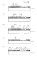
- Fig. 1 is an explanatory diagram showing a manufacturing process of forming a rewiring pattern by processing of a wafer level.
- Fig. 2 is an explanatory diagram showing a manufacturing process of forming an external connection terminal on the rewiring pattern by the processing of the wafer level.
- Fig. 3 is an explanatory diagram showing a method for sealing a surface on which the external connection terminal of a semiconductor wafer is formed by resin.
- Fig. 4 is an explanatory diagram showing an example of a semiconductor device formed by the processing of the wafer level.
- Fig. 5 is an explanatory diagram showing an example of an arrangement position (map) of semiconductor chips judged as nonconforming products by testing a semiconductor wafer.
- Fig. 6 is an explanatory diagram showing a state in which rewiring patterns are not formed in the semiconductor chips judged as the nonconforming products in the semiconductor wafer.
- Fig. 7 is an explanatory diagram showing an exemplary, non-limiting treatment method in which rewiring patterns are not formed in semiconductor chips judged as nonconforming products by applying a resist.
- Fig. 8 is an explanatory diagram showing a process of forming an external connection terminal on a semiconductor chip judged as a nonconforming product.
- Fig. 9 is an explanatory diagram showing an exemplary, non-limiting method for coating an undercoat metal layer by applying a resist to a region for forming a rewiring pattern.
- Fig. 10 is an explanatory diagram showing an exemplary, non-limiting treatment method in which rewiring patterns are not formed by applying a resist to semiconductor chips judged as nonconforming products in a semiconductor wafer.
- Fig. 11 is an explanatory diagram showing an exemplary, non-limiting treatment method in which a rewiring pattern is not formed with respect to a semiconductor chip judged as a nonconforming product using a negative resist.
- Fig. 12 is an explanatory diagram showing a state of performing treatment in which a rewiring pattern is not formed by irradiating a semiconductor chip judged as a nonconforming product in a semiconductor wafer with ultraviolet light.
- Fig. 13 is an explanatory diagram showing a state of performing burn-in of a semiconductor device.
- Fig. 14 is an explanatory diagram showing an exemplary, non-limiting method for manufacturing a semiconductor device by processing of a wafer level.
-
- Hereinafter, exemplary, non-limiting embodiments of the invention will be explained with reference to the accompanying drawings. In the present invention, terms are presumed to have their ordinary meaning as would be understood by one of ordinary skill in the relevant art. However, terms may also be operationally defined in this disclosure to have a specific meaning.
- Figs. 1 to 3 show a process example for forming a semiconductor device by a processing method of a wafer level. Fig. 1(a) shows a configuration of an electrode terminal formation surface of a
semiconductor wafer 10 in which anelectrode pad 14 is formed, and shows a state in which a surface of thesemiconductor wafer 10 is coated with apassivation film 12 and theelectrode pad 14 of aluminum is exposed from thepassivation film 12. Fig. 1(b) shows a state in which aninsulating layer 16 is formed on a surface of thepassivation film 12. The insulatinglayer 16 can be formed by coating the surface of thepassivation film 12 with an insulating material such as a polyimide film and exposing theelectrode pad 14. - Next, Fig. 1(c) shows a state in which surfaces of the
electrode pad 14 and the insulatinglayer 16 are coated with anundercoat metal layer 18. Theundercoat metal layer 18 is formed, for example, by sputtering chromium and then sputtering copper. - Fig. 1(d) shows a state in which a resist
pattern 20 for forming a rewiring pattern is formed on a surface of theundercoat metal layer 18 by a predetermined pattern. - Fig. 1(e) is a state in which copper plating is performed using the
undercoat metal layer 18 as a plating feeding layer and a conductor layer resulting in arewiring pattern 22 is formed on an exposed portion of theundercoat metal layer 18. Fig. 1(f) shows a state in which the resistpattern 20 is removed. Therewiring pattern 22 is formed in a state of being electrically connected to theelectrode pad 14. - Fig. 2 shows a process of forming an external connection terminal on the
rewiring pattern 22. Fig. 2 (a) shows a state in which a resistpattern 24 is formed so as to expose a region for forming an external connection terminal on therewiring pattern 22 in order to form the external connection terminal by plating. Numeral 24a is an exposure hole in which therewiring pattern 22 is exposed from the resistpattern 24. - Fig. 2 (b) shows a state in which copper plating is performed using the
undercoat metal layer 18 as a plating feeding layer and the copper plating is heaped up in the exposure hole 24a and acopper post 26 is formed. - Fig. 2(c) shows a state in which a
barrier metal layer 28 is covered and formed on an exposure end face of the top of thecopper post 26. Thebarrier metal layer 28 can be formed, for example, by performing nickel plating and gold plating in this order. - Fig. 2 (d) shows a state in which the resist
pattern 24 is removed. By removing the resistpattern 24, anexternal connection terminal 30 is exposed to the outside, and theundercoat metal layer 18 and therewiring pattern 22 formed on a surface of theundercoat metal layer 18 are exposed to a surface of thesemiconductor wafer 10. - Fig. 2(e) is a state in which an exposure portion of the
undercoat metal layer 18 is etched and the insulatinglayer 16 is exposed to a surface of thesemiconductor wafer 10, and therewiring pattern 22 is formed on a surface of the insulatinglayer 16 in a predetermined independent pattern. A region coated with therewiring pattern 22 in theundercoat metal layer 18 is left on the insulatinglayer 16, and therewiring pattern 22 is electrically connected to theelectrode pad 14 and theexternal connection terminal 30 is electrically connected to theelectrode pad 14 through therewiring pattern 22. - Fig. 3 shows a process of sealing an electrode terminal formation surface of the
semiconductor wafer 10 in which theexternal connection terminal 30 described above is formed by resin. - Fig. 3(a) shows a state in which the
semiconductor wafer 10 in which theexternal connection terminal 30 is formed is set in the side of a lower mold of a resin sealing apparatus.Numeral 40 is an upper mold, and numeral 41 is an inside lower mold, and numeral 42 is an outside lower mold.Numeral 43 is a temporary film for coating a molding surface of theupper mold 40. Thesemiconductor wafer 10 is arranged in a state in which a surface in which theexternal connection terminal 30 is formed is directed toward theupper mold 40, and aresin tablet 44 is supplied on thesemiconductor wafer 10. - Fig. 3 (b) shows a state in which clamping of the
semiconductor wafer 10 is started by a metal mold. After the outer periphery of thesemiconductor wafer 10 is closed by theupper mold 40 and the outsidelower mold 42, thesemiconductor wafer 10 together with theresin tablet 44 are clamped by the insidelower mold 41 and theupper mold 40, andresin 44a melted by heating is gradually charged into acavity 45. - Fig. 3(c) shows a state in which the metal mold is clamped to a mold clamping position and the
resin 44a is fully charged into thewhole cavity 45 and thesemiconductor wafer 10 is compressed and molded. - Fig. 3 (d) shows a state in which the mold is opened after the
resin 44a hardens. Thus, the surface of thesemiconductor wafer 10 in which theexternal connection terminal 30 is formed is fully sealed by theresin 44a. By the resin sealing through thetemporary film 43, an end face of theexternal connection terminal 30 is exposed to a surface of theresin 44a. - After the surface of the
semiconductor wafer 10 in which theexternal connection terminal 30 is formed is sealed by theresin 44a, thetemporary film 43 is peeled and asolder ball 46 is joined to the end face of theexternal connection terminal 30. Thereafter, semiconductor device of individual segments canbe obtained by cutting thesemiconductor wafer 10 together with theresin 44a every area of semiconductor chips. - Fig. 4(a) shows a state of joining the
solder ball 46 to the end face of theexternal connection terminal 30 and a configuration of a semiconductor device 50 (chip size package) in which thesemiconductor wafer 10 is cut into individual segments. Numeral 10a is a semiconductor chip cut into individual segments. - Fig. 4(b) enlarges and shows a state in which the surface of the
semiconductor device 50 in which theexternal connection terminal 30 is formed is sealed by theresin 44a and thesolder ball 46 and theexternal connection terminal 30 are electrically connected to theelectrode pad 14 of the semiconductor chip through therewiring pattern 22. - The manufacturing method of the semiconductor device described above shows an example of a manufacturing process of manufacturing the semiconductor device by processing of a wafer level. A manufacturing method of a semiconductor device according to the present invention is characterized in that in the case of performing a treatment for forming the
rewiring pattern 22 or forming theexternal connection terminal 30 at the wafer level as described above, on the basis of results in which individual semiconductor chips are inspected at a stage of manufacturing thesemiconductor wafer 10, a treatment different from treatment with respect to a semiconductor chip judged as a conforming product described above is performed with respect to a semiconductor chip judged as a nonconforming product. - That is, in the related art, in the case of the wafer level processing, the
rewiring pattern 22 is formed or a plating treatment is performed in like manner with respect to all the semiconductor chips of the semiconductor wafer. However, in the present invention, with respect to a semiconductor chip judged as a nonconforming product by inspection at the stage of manufacturing the semiconductor wafer, a treatment different from that of a semiconductor chip of a conforming product is performed so as not to damage an inspection apparatus or have adverse influence on a semiconductor device of a conforming product in the case of a treatment such as burn-in or an inspection after forming the semiconductor device by forming therewiring pattern 22 or theexternal connection terminal 30 and performing sealing by resin. - The treatment different from treatment with respect to a semiconductor chip of a conforming product refers to a treatment performed so as not to damage an inspection apparatus in the case of an inspection after forming a semiconductor device or have adverse influence on a semiconductor device of a conforming product in the case of burn-in. For example, there is a treatment in which an inspection apparatus or a burn-in apparatus is completely electrically disconnected from a semiconductor chip of a nonconforming product in order to avoid a problem that the semiconductor chip of the nonconforming product is electrically short-circuited and an overcurrent flows at the time of inspection.
- Fig. 5 shows a result (wafer electrical nonconformity map) of judging conformity and nonconformity of semiconductor chips by testing electrical characteristics etc. of individual semiconductor chips at a manufacturing stage of a semiconductor wafer. Fig. 5 shows the semiconductor chips in which division portions described as F are judged as nonconformity.
- Fig. 6 explanatorily shows a state of forming rewiring patterns on an electrode terminal formation surface of the
semiconductor wafer 10. Fig. 6 shows that the rewiring patterns are not formed in regions of the semiconductor chips judged as nonconformity in Fig. 5. Incidentally, for convenience of description, external connection terminals are not shown with respect to the semiconductor chips judged as nonconformity in Fig. 6. By being constructed so as not to form therewiring patterns 22 with respect to the semiconductor chips judged as nonconforming products, an inspection apparatus or a burn-in apparatus is electrically disconnected from the semiconductor chips and the semiconductor chips of the nonconforming products do not have adverse influence on the inspection apparatus or the burn-in apparatus. - Fig. 7 shows one exemplary, non-limiting example of a method constructed so that
rewiring patterns 22 are not electrically connected to electrodepads 14 with respect to regions of semiconductor chips judged as nonconforming products in the case of forming therewiring patterns 22 on the electrode terminal formation surface of thesemiconductor wafer 10 shown in Figs. 1 to 4 described above. - That is, Fig. 7 (a) shows a state in which an insulating
layer 16 is formed on a surface of asemiconductor wafer 10, and Fig. 7 (b) shows a state in which a surface of thesemiconductor wafer 10 is coated with anundercoat metal layer 18, and Fig. 7(c) shows a state in which a resistpattern 20 is formed so as to expose a region for forming arewiring pattern 22 on a surface of theundercoat metal layer 18. These processes are the same as the processes from Fig. 1(a) to Fig. 1(c). - In the present method, after the process of Fig. 7(c), with respect to a region of a semiconductor chip judged as nonconformity, in order to form the
rewiring pattern 22, a resist 20a is dropped to a region to which theundercoat metal layer 18 is exposed so that the region to which theundercoat metal layer 18 is exposed is coated as shown in Fig. 7(d). - Fig. 9 shows a state in which a resist
pattern 20 is formed on a surface of anundercoat metal layer 18 by a perspective view. Fig. 9 (a) shows a state in which a resist 20a is dropped to a region to which theundercoat metal layer 18 is exposed in order to form arewiring pattern 22, and Fig. 9 (b) shows a state in which the region to which theundercoat metal layer 18 is exposed is coated with the resist 20a. Since the region to which theundercoat metal layer 18 is exposed is formed in groove shape, the resist 20a flows along the groove and the resist 20a flows so as to bury the groove and the region ofundercoat metal layer 18 is coated. - Incidentally, when an exposed portion forming the
rewiring pattern 22 is coated with the resist 20a, it is unnecessary to coat the whole area of a surface of a semiconductor chip judged as nonconformity with the resist 20a. A method for coating only a portion forming a requiredrewiring pattern 22 so that an electrical short circuit does not occur in the case of testing a semiconductor device may be used. - Fig. 10 shows a state in which using a
nozzle 60, a resist 20a is applied to regions of semiconductor chips judged as nonconforming products in asemiconductor wafer 10 based on results of inspecting individual semiconductor chips at a manufacturing stage of a semiconductor wafer. Since the inspection results of the semiconductor wafer are stored as map data, thesemiconductor wafer 10 in which a resistpattern 20 is formed is sucked and supported on anX-Y stage 62 and based on the map data of the inspection results of thesemiconductor wafer 10, the semiconductor chips of the nonconforming products are aligned with thenozzle 60 and the resist 20a is applied to surfaces of the semiconductor chips. Therefore, a treatment shown in Fig. 7(d) can be performed with respect to all the semiconductor chips judged as the nonconforming products in thesemiconductor wafer 10. - Fig. 7 (e) is a process of forming a conductor layer resulting in the
rewiring pattern 22 on an exposed surface of theundercoat metal layer 18 using theundercoat metal layer 18 as a plating feeding layer. In Fig. 7(e), theundercoat metal layer 18 is coated with the resist 20a, so that the conductor layer is not formed on a surface of theundercoat metal layer 18. On the other hand, therewiring pattern 22 is formed on the surface of theundercoat metal layer 18 with respect to a semiconductor chip judged as a conforming product as shown in Fig. 1(e). - After a process of forming the
rewiring pattern 22, the resistpattern 20 is removed. Fig. 7 (f) shows a state of removing the resistpattern 20 and the resist 20a. - After removing the resist
pattern 20 and the resist 20a, anexternal connection terminal 30 is formed in the same process as the process shown in Fig. 2. A process of forming theexternal connection terminal 30 is shown in Fig. 8. In a manner similar to the process shown in Fig. 2, a resistpattern 24 is formed (Fig. 8 (a)) and acopper post 26 is formed by plating using theundercoat metal layer 18 as a plating feeding layer (Fig. 8 (b)) and theexternal connection terminal 30 is formed. As shown in Fig. 2, theexternal connection terminal 30 is formed on therewiring pattern 22 with respect to a semiconductor chip of a conforming product. On the other hand, theexternal connection terminal 30 is formed on theundercoat metal layer 18 without intervention of a conductor layer resulting in therewiring pattern 22 with respect to a semiconductor chip of a nonconforming product (Fig. 8(c)). - After forming the
external connection terminal 30, theundercoat metal layer 18 is etched and removed. Therefore, with respect to a region in which the semiconductor chip of the nonconforming product is formed, theundercoat metal layer 18 remains in only a region in which theexternal connection terminal 30 is formed so that theexternal connection terminal 30 is electrically disconnected from an electrode pad 14 (Fig. 8(d)). - Formation of the
external connection terminal 30 with respect to the semiconductor chip judged as the nonconforming product in thesemiconductor wafer 10 thus has an advantage capable of forming theexternal connection terminal 30 made of thecopper post 26 with normal shape. When theexternal connection terminal 30 made of thecopper post 26 is formed by electrolytic plating, a process is adjusted so that plating conditions (current density or plating deposition speed) on the semiconductor wafer become uniform in each of the regions (the center and periphery of the wafer) of the semiconductor wafer. Therefore, in the case of being constructed so that thecopper post 26 is not formed on a nonconforming chip, the plating conditions in each of the regions on the semiconductor wafer become nonuniform and thecopper post 2 6 with normal shape cannot be formed on a conforming chip. On the other hand, in the method of the present embodiment, thecopper post 26 is formed even when therewiring pattern 22 is not formed, so that such a problem can be avoided. - Incidentally, in the embodiment, plating of the rewiring pattern is not performed on the nonconforming chip, so that the plating conditions on the semiconductor wafer become nonuniform strictly. However, a plating thickness (5 to 10 µm) of the rewiring pattern is very thin as compared with a height (about 100 µm) of the copper post, so that there is no problem actually.
- Also, the
external connection terminals 30 are formed on the nonconforming chips, so that theexternal connection terminals 30 are uniformly present on the semiconductor wafer. Hence, in the case ofmakinginspectionofburn-inetc. on a semiconductor device, contact pressure of a contact probe of an inspection apparatus becomes uniform on the external connection terminals of each of the regions on the semiconductor wafer and connection between each of the external connection terminals and the contact probe can be made well and accurate inspection can be made. - Also, by forming the
external connection terminals 30 on the nonconforming chips, it is unnecessary to change a metal mold for sealing thesemiconductor wafer 10 by resin and there is also an advantage capable of using a related-art apparatus without change. - Fig. 11 shows an exemplary, non-limiting example of manufacture using a negative type resist as a method in which a
rewiring pattern 22 is not formed with respect to a semiconductor chip judged as a nonconforming product. Fig. 11 (a) and 11 (b) are the same process as that of Fig. 7 (a) and 7 (b) and show a process of forming an insulatinglayer 16 on a surface of asemiconductor wafer 10 and further forming anundercoat metal layer 18. Fig. 11(c) shows a state in which a surface of theundercoat metal layer 18 is coated with a negative resist 20b in order to form therewiring pattern 22. - For the negative resist, a region irradiated with light remains. Therefore, with respect to a semiconductor chip of a conforming product, it is constructed so as not to irradiate a region for forming the
rewiring pattern 22 with light using a mask. On the other hand, with respect to a semiconductor chip of a nonconforming product, it is constructed so as to irradiate the region for forming therewiring pattern 22 with focused light such as laser light as shown in Fig. 11 (d). - Fig. 12 shows a state in which a position of a semiconductor chip judged as a nonconforming product is irradiated with light (ultraviolet light) in a spot manner in a state (state of Fig. 11(c)) of coating a surface of a
semiconductor wafer 10 with the negative resist 20b based on inspection results at a manufacturing stage of thesemiconductor wafer 10. The semiconductor chip judged as the nonconforming product can be irradiated with the light from alight source 64 by positioning and moving thesemiconductor wafer 10 by anX-Y stage 62 based on map data of the inspection results of thesemiconductor wafer 10. Since an operation of irradiating the semiconductor chip of the nonconforming product with light so that the resist remains in a region for forming arewiring pattern 22 can be performed by adding a spot light irradiation process after an exposure process using a mask for forming a predetermined resistpattern 20, there is an advantage that a work load is small. - Also in the case by this method, the
rewiring pattern 22 is not formed with respect to the semiconductor chip judged as the nonconforming product and in a manner completely similar to the process shown in Figs. 7 and 8, the semiconductor chip judged as the nonconforming product can be rendered a state in which anelectrode pad 14 is electrically disconnected from anexternal connection terminal 30. - Fig. 13 shows a state of performing burn-in after a surface on which an
external connection terminal 30 of asemiconductor wafer 10 is formed is sealed byresin 44a.Numeral 70 is a support chuck of thesemiconductor wafer 10, and numeral 72 is a contactor, andnumerals 74 are contact bumps (contact probes). In a burn-in operation, thesemiconductor wafer 10 after resin sealing is clamped by thesupport chuck 70 and thecontactor 72 and is heated inside an oven and also the contact bumps 74 are pressed and contacted to theexternal connection terminals 30 of respective semiconductor device and a voltage higher than a normal working voltage is applied. - In Fig. 13, numeral 50 is a semiconductor device in which a
semiconductor chip 10a is judged as a conforming product and numeral 51 is a semiconductor device in which asemiconductor chip 10b is judged as a nonconforming product. It is shown that anelectrode pad 14 is electrically connected to theexternal connection terminal 30 through arewiring pattern 22 in thesemiconductor device 50 made of thesemiconductor chip 10a of the conforming product. Also, it is shown that theelectrode pad 14 is electrically disconnected from theexternal connection terminal 30 in thesemiconductor device 51 made of thesemiconductor chip 10b of the nonconforming product. As described above, by forming theexternal connection terminal 30 with respect to the semiconductor chip judged as the nonconforming product in a manner similar to the conforming product, thesemiconductor wafer 10 can surely be clamped by thesupport chuck 70 and thecontactor 72. - According to the manufacturing method of the semiconductor device of the present invention, as described above, the
semiconductor chip 10b is electrically disconnected from theexternal connection terminal 30 with respect to thesemiconductor device 51 made of thesemiconductor chip 10b judged as the nonconforming product. Therefore, thecontactor 72 is electrically separated from thesemiconductor chip 10b judged as the nonconforming product and an overcurrent can be prevented from flowing in thesemiconductor chip 10b. Therefore, a burn-in apparatus is not damaged and adverse influence on thesemiconductor chip 10a of the conforming product in the vicinity due to overheating of the semiconductor chip of the nonconforming product can be prevented. - Incidentally, a method for manufacturing a semiconductor device by processing of a wafer level is not limited to the manufacturing method described above, and can also be achieved by other methods, and a form of a chip size package also includes several kinds.
- For example, in the method described above, the
undercoat metal layer 18 is formed and the conductor layer resulting in therewiring pattern 22 is formed and then thecopper post 26 resulting in theexternal connection terminal 30 is formed by copper plating. However, instead of forming thecopper post 26, there is also a method for forming an external connection terminal by merely joining a solder ball to arewiring pattern 22. Its manufacturing method is shown in Fig. 14. - Fig. 14(a) shows a state in which a
rewiring pattern 22 is formed on a surface of asemiconductor wafer 10 in a manner similar to the method shown in Figs. 1 (a) to 1 (f). Fig. 14 (b) shows a state in which a polyimide film etc. are laminated on the surface of thesemiconductor wafer 10 to form an insulatingfilm 32 and a pad 22a for joining a solder ball is exposed. Fig. 14 (c) is a state of forming an external connection terminal by joining asolder ball 34 to the pad 22a. - Also for this manufacturing method, in this case of forming a resist pattern for forming the rewiring pattern on a surface of the undercoat metal layer, in a manner similar to that shown in Fig. 10 or Fig. 12, with respect to a semiconductor chip judged as a nonconforming product, a region for forming the rewiring pattern is not exposed to the
undercoat metal layer 18 so as not to form the rewiring pattern and thereby the rewiring pattern is not formed and thesolder ball 34 is not joined and it can be rendered a state in which the solder ball and anelectrode pad 14 are electrically disconnected from the outside. Fig. 14 (d) shows a situation in which with respect to a region in which a nonconforming semiconductor chip is formed, a metal layer such as the rewiring pattern is not formed and the insulatinglayer 16 is exposed. Therefore, the solder ball is not joined to an opening 32a of the insulatingfilm 32 after forming the insulating film 32 (Fig. 14(e)). - Thus, even in the case of different forms of the semiconductor device or different manufacturing methods, with respect to a semiconductor chip judged as a nonconforming product, required treatment is previously performed in the case of a process of forming a rewiring pattern at a wafer level so as not to have adverse influence on an inspection apparatus or a burn-in apparatus etc. after assembling the semiconductor device. Therefore, more accurate inspection can be performed and problems of having adverse influence on the inspection apparatus or having adverse influence on a semiconductor device of a conforming product can be avoided.
- Incidentally, the embodiment described above shows the example of avoiding a situation in which an inspection apparatus etc. in a post-process are directly electrically connected to a semiconductor chip judged as a nonconforming product by previous inspection by means of a method applicable in a related-art manufacturing process of a semiconductor device of a wafer level. However, a method for electrically disconnecting the semiconductor chip of the nonconforming product from the inspection apparatus etc. is not limited to the method of the embodiment described above. For example, a method for forming a dummy external connection terminal with the same form as that of an
external connection terminal 30 by burying a resin material made of an electrical insulator in an exposure hole 24a so that acopper post 26 is not formed with respect to a semiconductor chip of a nonconforming product in the case of forming theexternal connection terminal 30 can also be used. In this case, arewiring pattern 22 may be formed also with respect to the semiconductor chip of the nonconforming product.
Claims (5)
- A method for manufacturing a semiconductor device (10a) by processing of a wafer level, the method comprising: in the case of forming the semiconductor device at the wafer level,
performing a treatment for forming a circuit including a rewiring pattern (22) with respect to a semiconductor chip (10a) judged as a conforming product on the basis of inspection results on individual semiconductor chips constituting a semiconductor wafer (10); and
performing a treatment for avoiding having adverse influence on the semiconductor device (10a) of the conforming product or an inspection apparatus in an inspection of a formed semiconductor device after forming the semiconductor device with respect to a semiconductor chip judged as a nonconforming product on the basis of the inspection results on individual semiconductor chips. - A manufacturing method of a semiconductor device as claimed in claim 1, wherein the treatment for avoiding having the adverse influence with respect to the semiconductor chip judged as the nonconforming product includes a treatment in which said semiconductor chip is electrically disconnected from a circuit electrically connected to an electrode pad of the semiconductor chip.
- A manufacturing method of a semiconductor device as claimed in claim 1 or 2, wherein the treatment for forming the circuit with respect to the semiconductor chip judged as the conforming product includes a treatment in which a rewiring pattern for electrically connecting an electrode pad of the semiconductor chip to an external connection terminal is formed, and
the treatment for avoiding having the adverse influence with respect to the semiconductor chip judged as the nonconforming product includes a treatment in which the rewiring pattern is not formed and it is formed in a state of electrically disconnecting the electrode pad of the semiconductor chip from the external connection terminal. - A manufacturing method of a semiconductor device as claimed in claim 3, wherein the treatment in which the rewiring pattern is not formed with respect to the semiconductor chip judged as the nonconforming product includes forming an undercoat metal layer on an electrode terminal formation surface of the semiconductor wafer, forming a resist pattern, to which a region for forming the rewiring pattern electrically connected to the electrode pad of the semiconductor chip is exposed, on a surface of the undercoat metal layer, applying a resist to the region for forming the rewiring pattern resist with respect to the semiconductor chip judged as the nonconforming product so that the region for forming the rewiring pattern is coated with the resist, and forming a conductor layer resulting in the rewiring pattern in only the semiconductor chip judged as the conforming product by performing a plating using the undercoat metal layer as a plating feeding layer with respect to the semiconductor wafer.
- A manufacturing method of a semiconductor device as claimed in claim 3 or 4, wherein the treatment in which the rewiring pattern is not formed with respect to the semiconductor chip judged as the nonconforming product includes forming an undercoat metal layer on an electrode terminal formation surface of the semiconductor wafer, forming a resist pattern, to which a region for forming the rewiring pattern electrically connected to the electrode pad of the semiconductor chip is exposed, on a surface of the undercoat metal layer so as to coat the region for forming the rewiring pattern with respect to the semiconductor chip judged as the non conforming product, and forming a conductor layer resulting in the rewiring pattern in only the semiconductor chip judged as the conforming product by performing a plating using the undercoat metal layer as a plating feeding layer with respect to the semiconductor wafer.
Applications Claiming Priority (2)
| Application Number | Priority Date | Filing Date | Title |
|---|---|---|---|
| JP2004050652A JP4217639B2 (en) | 2004-02-26 | 2004-02-26 | Manufacturing method of semiconductor device |
| JP2004050652 | 2004-02-26 |
Publications (2)
| Publication Number | Publication Date |
|---|---|
| EP1569270A2 true EP1569270A2 (en) | 2005-08-31 |
| EP1569270A3 EP1569270A3 (en) | 2010-09-01 |
Family
ID=34747485
Family Applications (1)
| Application Number | Title | Priority Date | Filing Date |
|---|---|---|---|
| EP05004336A Withdrawn EP1569270A3 (en) | 2004-02-26 | 2005-02-28 | Manufacturing method of semiconductor device |
Country Status (5)
| Country | Link |
|---|---|
| US (1) | US7186575B2 (en) |
| EP (1) | EP1569270A3 (en) |
| JP (1) | JP4217639B2 (en) |
| KR (1) | KR101117617B1 (en) |
| TW (1) | TWI364778B (en) |
Families Citing this family (8)
| Publication number | Priority date | Publication date | Assignee | Title |
|---|---|---|---|---|
| US7049526B2 (en) * | 2003-11-03 | 2006-05-23 | Intel Corporation | Microvia structure and fabrication |
| US7749882B2 (en) | 2006-08-23 | 2010-07-06 | Micron Technology, Inc. | Packaged microelectronic devices and methods for manufacturing packaged microelectronic devices |
| TWI451546B (en) * | 2010-10-29 | 2014-09-01 | 日月光半導體製造股份有限公司 | Stacked package structure, package structure thereof and manufacturing method of package structure |
| JP2014036165A (en) * | 2012-08-09 | 2014-02-24 | Shinko Electric Ind Co Ltd | Semiconductor device |
| US8906743B2 (en) | 2013-01-11 | 2014-12-09 | Micron Technology, Inc. | Semiconductor device with molded casing and package interconnect extending therethrough, and associated systems, devices, and methods |
| KR101707931B1 (en) * | 2015-08-07 | 2017-02-17 | 주식회사 에스에프에이반도체 | Wafer level package with redistribution layer for measuring electrical resistance and method for testing electricproperties of the wafer level package by using the redistribution layer |
| CN109218483A (en) * | 2018-11-16 | 2019-01-15 | 东莞市沃德精密机械有限公司 | Automatic placement equipment |
| JP2022138014A (en) * | 2021-03-09 | 2022-09-22 | キオクシア株式会社 | Method for manufacturing semiconductor device, semiconductor manufacturing system, and semiconductor device |
Citations (2)
| Publication number | Priority date | Publication date | Assignee | Title |
|---|---|---|---|---|
| JP2001093927A (en) | 1999-09-21 | 2001-04-06 | Matsushita Electric Ind Co Ltd | Semiconductor device, method of manufacturing the same, and burn-in device |
| US20020139976A1 (en) | 2001-04-02 | 2002-10-03 | Hembree David R. | Method for fabricating semiconductor components |
Family Cites Families (6)
| Publication number | Priority date | Publication date | Assignee | Title |
|---|---|---|---|---|
| JP3356921B2 (en) | 1995-03-24 | 2002-12-16 | 新光電気工業株式会社 | Semiconductor device and method of manufacturing the same |
| JP3137322B2 (en) | 1996-07-12 | 2001-02-19 | 富士通株式会社 | Semiconductor device manufacturing method, semiconductor device manufacturing mold, and semiconductor device |
| TW498468B (en) * | 1999-10-29 | 2002-08-11 | Hitachi Ltd | Semiconductor device |
| TW577152B (en) | 2000-12-18 | 2004-02-21 | Hitachi Ltd | Semiconductor integrated circuit device |
| US6395622B1 (en) * | 2001-06-05 | 2002-05-28 | Chipmos Technologies Inc. | Manufacturing process of semiconductor devices |
| JP2004031463A (en) | 2002-06-24 | 2004-01-29 | Matsushita Electric Ind Co Ltd | Inspection method for semiconductor integrated circuit |
-
2004
- 2004-02-26 JP JP2004050652A patent/JP4217639B2/en not_active Expired - Fee Related
-
2005
- 2005-02-23 KR KR1020050014996A patent/KR101117617B1/en not_active Expired - Fee Related
- 2005-02-23 US US11/064,500 patent/US7186575B2/en not_active Expired - Lifetime
- 2005-02-25 TW TW094105854A patent/TWI364778B/en not_active IP Right Cessation
- 2005-02-28 EP EP05004336A patent/EP1569270A3/en not_active Withdrawn
Patent Citations (2)
| Publication number | Priority date | Publication date | Assignee | Title |
|---|---|---|---|---|
| JP2001093927A (en) | 1999-09-21 | 2001-04-06 | Matsushita Electric Ind Co Ltd | Semiconductor device, method of manufacturing the same, and burn-in device |
| US20020139976A1 (en) | 2001-04-02 | 2002-10-03 | Hembree David R. | Method for fabricating semiconductor components |
Non-Patent Citations (1)
| Title |
|---|
| LAU J H: "Low Cost Flip Chip Technologies", 2000, MCGRAW-HILL, article "Chapter 10.2.1: WLCSP redistribution and bumping", pages: 318 - 320 |
Also Published As
| Publication number | Publication date |
|---|---|
| KR20060043142A (en) | 2006-05-15 |
| JP2005243860A (en) | 2005-09-08 |
| TW200535943A (en) | 2005-11-01 |
| JP4217639B2 (en) | 2009-02-04 |
| US7186575B2 (en) | 2007-03-06 |
| US20050191772A1 (en) | 2005-09-01 |
| EP1569270A3 (en) | 2010-09-01 |
| KR101117617B1 (en) | 2012-03-07 |
| TWI364778B (en) | 2012-05-21 |
Similar Documents
| Publication | Publication Date | Title |
|---|---|---|
| US6432752B1 (en) | Stereolithographic methods for fabricating hermetic semiconductor device packages and semiconductor devices including stereolithographically fabricated hermetic packages | |
| US7064445B2 (en) | Wafer level testing and bumping process | |
| US6297658B1 (en) | Wafer burn-in cassette and method of manufacturing probe card for use therein | |
| US6794224B2 (en) | Semiconductor device including leads in communication with contact pads thereof and a stereolithographically fabricated package substantially encapsulating the leads and methods for fabricating the same | |
| KR100681772B1 (en) | Semiconductor test method and semiconductor test device | |
| JPH08504036A (en) | Area array wiring chip TAB test | |
| US7186575B2 (en) | Manufacturing method of semiconductor device | |
| KR100216840B1 (en) | Printed Circuit Board Strips for Semiconductor Packages | |
| CN110494964A (en) | Semiconductor packages with exposed redistribution layer features and related packaging and testing methods | |
| US20240194542A1 (en) | Substrate including test circuit and substrate test apparatus including the substrate | |
| TW201530723A (en) | Method for processing the surface of a lead frame and device having a treated lead frame surface | |
| US6002267A (en) | In-line voltage plane tests for multi-chip modules | |
| KR100324939B1 (en) | Printed Circuit Boards for Semiconductor Packages to Prevent Static | |
| JP2001118994A (en) | Semiconductor device | |
| JPH1164389A (en) | Method of manufacturing bump type contactor and contact for bump type contactor | |
| CN115101421B (en) | Packaging method of wafer level chip | |
| KR102763456B1 (en) | Method of manufacturing probe tip and probe tip manufactured by the same | |
| CN100392809C (en) | Method for manufacturing wafer insulating layer interconnect and structure thereof | |
| EP4345866A1 (en) | A method and a system for manufacturing an assembly of a power semiconductor | |
| US7253093B2 (en) | Method for fabricating interconnection in an insulating layer on a wafer | |
| JP2839686B2 (en) | Film carrier tape and semiconductor device using this film carrier tape | |
| CN119542304A (en) | Integrated circuit with improved ball bond adhesion | |
| CN119695038A (en) | Chip carriers, lead frames and packaging devices | |
| CN121385391A (en) | Improved identification of poor quality welded joints | |
| CN113097084A (en) | Method for exposing metal layer and circuit repairing method |
Legal Events
| Date | Code | Title | Description |
|---|---|---|---|
| PUAI | Public reference made under article 153(3) epc to a published international application that has entered the european phase |
Free format text: ORIGINAL CODE: 0009012 |
|
| AK | Designated contracting states |
Kind code of ref document: A2 Designated state(s): AT BE BG CH CY CZ DE DK EE ES FI FR GB GR HU IE IS IT LI LT LU MC NL PL PT RO SE SI SK TR |
|
| AX | Request for extension of the european patent |
Extension state: AL BA HR LV MK YU |
|
| PUAL | Search report despatched |
Free format text: ORIGINAL CODE: 0009013 |
|
| AK | Designated contracting states |
Kind code of ref document: A3 Designated state(s): AT BE BG CH CY CZ DE DK EE ES FI FR GB GR HU IE IS IT LI LT LU MC NL PL PT RO SE SI SK TR |
|
| AX | Request for extension of the european patent |
Extension state: AL BA HR LV MK YU |
|
| 17P | Request for examination filed |
Effective date: 20110214 |
|
| AKX | Designation fees paid |
Designated state(s): DE FR |
|
| 17Q | First examination report despatched |
Effective date: 20130227 |
|
| STAA | Information on the status of an ep patent application or granted ep patent |
Free format text: STATUS: THE APPLICATION IS DEEMED TO BE WITHDRAWN |
|
| 18D | Application deemed to be withdrawn |
Effective date: 20140829 |