EP1569045A2 - Stromversorgung für ein Bilderzeugungssystem mit hybrider berührungsloser Entwicklung - Google Patents
Stromversorgung für ein Bilderzeugungssystem mit hybrider berührungsloser Entwicklung Download PDFInfo
- Publication number
- EP1569045A2 EP1569045A2 EP05100350A EP05100350A EP1569045A2 EP 1569045 A2 EP1569045 A2 EP 1569045A2 EP 05100350 A EP05100350 A EP 05100350A EP 05100350 A EP05100350 A EP 05100350A EP 1569045 A2 EP1569045 A2 EP 1569045A2
- Authority
- EP
- European Patent Office
- Prior art keywords
- voltage
- donor
- image
- power supply
- marking particles
- Prior art date
- Legal status (The legal status is an assumption and is not a legal conclusion. Google has not performed a legal analysis and makes no representation as to the accuracy of the status listed.)
- Withdrawn
Links
Images


Classifications
-
- G—PHYSICS
- G03—PHOTOGRAPHY; CINEMATOGRAPHY; ANALOGOUS TECHNIQUES USING WAVES OTHER THAN OPTICAL WAVES; ELECTROGRAPHY; HOLOGRAPHY
- G03G—ELECTROGRAPHY; ELECTROPHOTOGRAPHY; MAGNETOGRAPHY
- G03G15/00—Apparatus for electrographic processes using a charge pattern
- G03G15/06—Apparatus for electrographic processes using a charge pattern for developing
- G03G15/08—Apparatus for electrographic processes using a charge pattern for developing using a solid developer, e.g. powder developer
- G03G15/0803—Apparatus for electrographic processes using a charge pattern for developing using a solid developer, e.g. powder developer in a powder cloud
Definitions
- This invention relates to the field of electrophotographic image forming systems and power supplies used therewith.
- Hybrid Scavengeless Development is a process for ionographic or electrophotographic imaging and printing apparatuses designed to prevent scavenging of toner from the photoreceptor of the imaging device by subsequent development stations.
- the process of electrophotographic printing includes charging a photoconductive member to a substantially uniform potential to sensitize the surface.
- the charged photoconductive surface is exposed to a light image from either a scanning laser beam, an LED source, or an original document being reproduced.
- This records an electrostatic latent image on the photoconductive surface.
- the latent image is developed.
- Two-component and single-component developer materials are commonly used for development.
- a typical two-component developer comprises magnetic carrier granules having toner particles adhering triboelectrically thereto.
- a single-component developer material typically comprises toner particles. Toner particles are attracted to the latent image, forming a toner powder image on the photoconductive surface. The toner powder image is subsequently transferred to a copy sheet. Finally, the toner powder image is heated to permanently fuse it to the copy sheet in image configuration.
- the electrophotographic marking process discussed above can be modified to produce color images.
- One color electrophotographic marking process called image-on-image (IOI) processing, superimposes toner powder images of different color toners onto the photoreceptor prior to the transfer of the composite toner powder image onto the substrate.
- IOI image-on-image
- the viability of printing system concepts such as IOI processing requires development systems that do not interact with a previously toned image. Since several known development systems, such as conventional magnetic brush development and jumping single-component development, interact with the image on the receiver, a previously toned image will be scavenged by subsequent development if interacting development systems are used.
- scavengeless or non-interactive development systems For a thorough description of scavengeless development see U.S. Patent 5,031,570, hereby incorporated by reference in its entirety.
- Hybrid scavengeless development technology deposits toner via a conventional magnetic brush onto the surface of a donor roll and a plurality of electrode wires are closely spaced from the toned donor roll in the development zone. An AC voltage is applied to the electrode wires to generate a toner cloud in the development zone.
- This donor roll generally consists of a conductive core covered with a thin (50 -200 ⁇ m) partially conductive layer.
- the magnetic brush roll is held at an electrical potential difference relative to the donor core to produce the field necessary for toner development.
- the toner layer on the donor roll is then disturbed by electric fields from a wire or set of wires to produce and sustain an agitated cloud of toner particles.
- Typical ac voltages of the wires relative to the donor are 600-900 Vpp at frequencies of 5-15 kHz. These ac signals are often square waves, rather than pure sinusoidal waves. Toner from the cloud is then developed onto the nearby photoreceptor by fields created by a latent image.
- a problem inherent to developer systems using wires is a vibration of the wires parallel to the donor roll and photoreceptor surfaces.
- This wire vibration manifests itself in a density variation, at a frequency corresponding to the wire vibration frequency, of toner on the photoreceptor.
- higher harmonics of vibration being an integer multiple of the wire fundamental frequency, can be excited by the applied voltage frequency. Again these vibrations can cause a density variation, at a frequency corresponding to the wire vibration frequency to produce density variations that correspond to a harmonic standing wave patterns, of toner on the photoreceptor.
- fundamental strobing is the term used to describe the vibration and print defect associated with the fundamental mode of vibration
- harmonic strobing is used to describe the defect caused by the higher harmonics. Strobing does not occur at all hardware setpoints. For instance, it can often be reduced by decreasing the amplitude of the wire voltage, or varying the donor roll speed.
- fundamental strobing is related to the applied wire frequency in a complex manner, and both types of strobing are sensitive to the frictional properties of the toner.
- a power supply is separately provided for an HSD image forming system which includes frequency deviation capability for avoidance of wire strobing defects.
- a power supply is separately provided for an HSD image forming system which uses square waves instead of sinusoidal waves in generating toner clouds to increase the average voltage applied to the toner without increasing the peak voltage.
- a power supply is separately provided for an HSD image forming system which uses relatively low amplitude AC voltages, thus reducing power consumption and stress on toner concentration sensors.
- a power supply is separately provided for an HSD image forming system which utilizes asymmetric waveforms.
- the systems and methods according to this invention provides a power supply for a hybrid scavengeless development electrophotographic image forming system in which the donor roll and the wires are operated at the same AC voltage frequency without phase shifts, allowing the donor roll to be run at a higher voltage.
- the voltage signals supplied to the mag roller bias terminal, the donor roller bias terminal and the wire electrode are asymmetric with respect to the voltage axis.
- the signals supplied to the mag roller bias terminal, the donor roller bias terminal and the wire electrode bias terminal are in phase with one another.
- a method of operating a donor member and an associated alternating current biased electrode in a developer unit used for developing a latent image recorded on an image receiving member with marking particles, to form a developed image the developer having a magnetic brush member and a donor member, the donor member being spaced from the image receiving member, for transporting marking particles to a development zone adjacent the image receiving member; the alternating current biased electrode being positioned in the development zone between the image receiving member and the donor member; and a voltage supply for electrically biasing said electrode during a developing operation with an alternating and direct current voltage to detach marking particles from said donor member, forming a cloud of marking particles in the development zone, and developing the latent image with marking particles from the cloud, the method comprises:
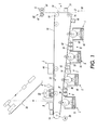
- Fig. 1 is a schematic view of an exemplary four color electrophotographic image forming device
- Fig. 2 is a detailed schematic view of a single color station in an exemplary multi-color scavengeless electrophotographic image forming device
- Fig. 3 is a block diagram of a power supply according to an exemplary embodiment of this invention.
- Fig. 4 is a graph illustrating toner transmission density versus frequency for sinusoidal and square AC wire voltages.
- Fig. 5 is a graph of the square wave AC voltages generated by the power supply according to an exemplary embodiment of this invention.
- An electrophotographic image forming device creates a color image in a single pass through the machine.
- the image forming device uses a charge retentive surface in the form of, for example, an Active Matrix (AMAT) photoreceptor belt 10 which travels sequentially through various process stations in the direction indicated by the arrow 12.
- AMAT Active Matrix
- Belt travel is brought about by mounting the belt about a drive roller 14 and two tension rollers 16 and 18 and then rotating the drive roller 14 via a drive motor 20.
- the image area is that part of the photoreceptor belt which is to receive the toner powder images that, after being transferred to a substrate, produce the final image. While the photoreceptor belt may have numerous image areas, since each image area is processed in the same way, a description of the typical processing of one image area suffices to fully explain the operation of the printing machine.
- a corona generating device As the photoreceptor belt 10 moves, the image area passes through a charging station A.
- a corona generating device indicated generally by the reference numeral 22, charges the image area to a relatively high and substantially uniform potential.
- the image area will be charged to a uniform potential of about -500 volts. In practice, this is accomplished by charging the image area slightly more negative than -500 volts so that any resulting dark decay reduces the voltage to the desired -500 volts. While this description refers to the image area as being negatively charged, it could be positively charged if the charge levels and polarities of the toners, recharging devices, photoreceptor, and other relevant regions or devices are appropriately changed.
- the now charged image area passes through a first exposure station B.
- the charged image area is exposed to light which illuminates the image area with a light representation of a first color (say black) image. That light representation discharges some parts of the image area so as to create an electrostatic latent image.
- a laser-based output scanning device 24 as a light source
- other light sources for example an LED printbar
- a voltage level of about -500 volts will exist on those parts of the image area which were not illuminated, while a voltage level of about -50 volts will exist on those parts which were illuminated.
- the image area has a voltage profile comprised of relative high and low voltages.
- the now exposed image area passes through a first development station C which is identical in structure with development systems E, G, and I.
- the first development station C deposits a first color, say black, of negatively charged toner 31 onto the image area. That toner is attracted to the less negative sections of the image area and repelled by the more negative sections. The result is a first toner powder image on the image area.
- a first color say black
- the exposed and unexposed areas of the photoreceptor are interchanged, or if the charging polarity of the photoreceptor is made positive.
- development system includes a donor roll 40.
- the electrode wires 42 are electrically biased with an AC and DC voltage relative to donor roll 40 for the purpose of detaching toner there from. This detached toner forms a toner powder cloud in the gap between the donor roll and photoconductive surface.
- Both the electrode wires 42 and the donor roll 40 are biased with DC sources 102 and 92 respectively for discharge area development (DAD).
- DAD discharge area development
- toner 76 (which generally represents any particular color of toner) adheres to the illuminated image area. This causes the voltage in the illuminated area to increase to, for example, about -200 volts. The non-illuminated parts of the image area remain at about the level of -500 volts.
- the recharging station D is comprised of two corona recharging devices, a first recharging device 36 and a second recharging device 37. These devices act together to recharge the voltage levels of both the toned and untoned parts of the image area to a substantially uniform level. It is to be understood that power supplies are coupled to the first and second recharging devices 36 and 37, and to any grid or other voltage control surface associated therewith, so that the necessary electrical inputs are available for the recharging devices to accomplish their task.
- the image area After the image area passes through the first recharging device 36, the image area is overcharged by the first recharging device to more negative levels than that which the image area is to have when it leaves the recharging station D.
- the toned and the untoned parts of the image area reach a voltage level of about -700 volts.
- the first recharging device 36 is preferably a DC scorotron.
- the image area After being recharged by the first recharging device 36, the image area passes to the second recharging device 37.
- the second recharging device 37 reduces the voltage of the image area, both the untoned parts and the toned parts (represented by toner 76) to the desired potential of -500 volts.
- the now substantially uniformly charged image area with its first toner powder image passes to a second exposure station 38.
- the second exposure station illuminates the image area with a light representation of a second color image (say yellow) to create a second electrostatic latent image
- the second exposure station 38 is the same as the first exposure station B.
- the non-illuminated areas have a potential of about -500 volts.
- illuminated areas both the previously toned areas denoted by the toner 76 and the untoned areas are discharged to about -50 volts.
- the image area then passes to a second development station E. Except for the fact that the second development station E contains a toner 40 which is of a different color (yellow) than the toner 31 (black) in the first development station C, the second development station is substantially the same as the first development station. Since the toner 40 is attracted to the less negative parts of the image area and repelled by the more negative parts, after passing through the second development station E the image area has first and second toner powder images which may overlap.
- the image area then passes to a second recharging station F.
- the second recharging station F has first and second recharging devices, the devices 51 and 52, respectively, which operate similar to the recharging devices 36 and 37.
- the first corona recharge device 51 overcharges the image areas to a greater absolute potential than that ultimately desired (say -700 volts) and the second corona recharging device, comprised of coronodes having AC potentials, neutralizes that potential to that ultimately desired.
- the now recharged image area then passes through a third exposure station 53. Except for the fact that the third exposure station illuminates the image area with a light representation of a third color image (say magenta) so as to create a third electrostatic latent image, the third exposure station 38 is the same as the first and second exposure stations B and 38.
- the third electrostatic latent image is then developed using a third color of toner 55 (magenta) contained in a third development station G.
- the now recharged image area then passes through a third recharging station H.
- the third recharging station includes a pair of corona recharge devices 61 and 62 which adjust the voltage level of both the toned and untoned parts of the image area to a substantially uniform level in a manner similar to the corona recharging devices 36 and 37 and recharging devices 51 and 52.
- the now recharged image area After passing through the third recharging station the now recharged image area then passes through a fourth exposure station 63. Except for the fact that the fourth exposure station illuminates the image area with a light representation of a fourth color image (say cyan) so as to create a fourth electrostatic latent image, the fourth exposure station 63 is the same as the first, second, and third exposure stations, the exposure stations B, 38, and 53, respectively.
- the fourth electrostatic latent image is then developed using a fourth color toner 65 (cyan) contained in a fourth development station I.
- the image area then passes to a pretransfer corotron member 50 which delivers corona charge to ensure that the toner particles are of the required charge level so as to ensure proper subsequent transfer.
- the four toner powder images are transferred from the image area onto a support sheet 57 at transfer station J.
- the transfer station J includes a transfer corona device 54 which sprays positive ions onto the backside of sheet 57. This causes the negatively charged toner powder images to move onto the support sheet 57.
- the transfer station J also includes a detack corona device 56 which facilitates the removal of the support sheet 52 from the printing machine.
- the fusing station K includes a fuser assembly, indicated generally by the reference numeral 60, which permanently affixes the transferred powder image to the support sheet 57.
- the fuser assembly 60 includes a heated fuser roller 67 and a backup or pressure roller 64.
- a chute guides the support sheets 57 to a catch tray, also not shown, for removal by an operator.
- the various machine functions described above are generally managed and regulated by a controller which provides electrical command signals for controlling the operations described above.
- development system 38 includes a donor roll 40.
- a development apparatus advances developer materials into development zones.
- the development system 38 is scavengeless. By scavengeless is meant that the developer or toner of system 38 must not interact with an image already formed on the image receiver. Thus, the system 38 is also known as a non-interactive development system.
- the development system 38 comprises a donor structure in the form of a roller 40.
- the donor structure 40 conveys a toner layer to the development zone which is the area between the member 10 and the donor structure 40.
- the toner layer 82 can be formed on the donor 40 by either a two-component developer (i.e. toner and carrier), as shown in FIG.
- the development zone contains an AC biased electrode structure 42 self-spaced from the donor roll 40 by the toner layer.
- the single-component toner may comprise positively or negatively charged toner.
- a conventional magnetic brush 46 also referred to below as “magnetic brush roll” and “mag roll,” is used for depositing the toner layer onto the donor structure.
- the magnetic brush 46 includes a magnetic core enclosed by a sleeve 86. The magnetic brush 46 is shown moving in a counter clockwise direction by arrow 85.
- auger 76 is located in housing 44. Auger 76 is mounted rotatably to mix and transport developer material.
- the augers 76 have blades extending spirally outwardly from a shaft. The blades are designed to advance the developer material in the axial direction substantially parallel to the longitudinal axis of the shaft.
- the developer metering device is designated 88. As successive electrostatic latent images are developed, the toner particles within the developer material are depleted.
- a toner dispenser (not shown) stores a supply of toner particles. The toner dispenser is in communication with housing 44. As the concentration of toner particles in the developer material is decreased, fresh toner particles are furnished to the developer material in the chamber from the toner dispenser.
- the augers 76 in the chamber of the housing mix the fresh toner particles with the remaining developer material so that the resultant developer material therein is substantially uniform with the concentration of toner particles being optimized. In this manner, a substantially constant amount of toner particles are maintained in the chamber of the developer housing.
- the electrode structure 42 is comprised of one or more thin (e.g., 50 to 100 micron diameter) conductive wires which are lightly positioned against the toner on the donor structure 40.
- the distance between the wires and the donor is self-spaced by the thickness of the toner layer, which may be approximately 15 microns.
- the extremities of the wires are supported by blocks (not shown) at points slightly above a tangent to the donor roll surface.
- Suitable scavengeless development systems for incorporation in the present invention are disclosed in U.S. Pat. No. 4,868,600 and in U.S. Pat. No. 6,101,357, both of which are hereby incorporated by reference in their entirety.
- a scavengeless development system may be conditioned to selectively develop one or the other of the two image areas (i.e. discharged and charged image areas) by the application of appropriate AC and DC voltage biases to the wires 42 and the donor roll structure 40.
- the developer system includes a power supply for applying AC and DC voltages to the electrode wires 42, donor roll 40 and mag roll 46.
- a conventional power supply is shown in FIG. 2.
- a DC voltage source 102 provides proper bias to the wires 42 relative to the donor roller 40.
- the electrode wires 42 receive AC voltages from sources 103 and 104. These sources may generate different frequencies, and the resultant voltage on the wire is the instantaneous sum of the AC sources 103 and 104 plus the DC source 102.
- the AC source 103 is often chosen to have the same frequency, magnitude, and phase as the AC source 96, which supplies the donor roll 40. Then, the voltage of the wires with respect to the donor roll is just that of the AC source 104 plus that of the DC source 102.
- the AC voltage source 104 is connected to a modulator 106 for modulating its frequency.
- the modulated frequency alternating voltage signal from that AC voltage source 104 is electrically connected to the electrode wires 42. If the AC voltage source 104 has a frequency output that can be controlled by an external voltage, the modulator 106 may be any suitable commercially available suitable device, such as one including a frequency generator.
- the AC voltage sources 104 and 103 and the DC voltage source 102 receive their power from the power supply 94, the power may likewise be received from separate power supplies.
- the DC voltage source 102 may be separate from the DC voltage sources 92 and 98 as shown in FIG. 2 or share a common voltage source.
- the AC voltage source 104 may be separate from the AC voltage sources 96, 103, and 100 as shown in FIG. 2 or share a common voltage source.
- modulator 106 may merely modulate the signal from the AC voltage source 104 as shown in FIG. 2 or modulate any of the AC voltage sources 96, 103, or 100.
- FIG. 2 The electrical sections of FIG. 2 are schematic in nature. Those skilled in the art of electronic circuits will realize there are many possible ways to connect AC and DC voltage sources to achieve the desired voltages on electrodes 42, donor roll 40, and magnetic brush roll 46.
- a power supply circuit 200 which provides improved performance over conventional power supplies used in scavengeless development image forming systems.
- at least three voltages are important in moving toner from the developer housing to the photoreceptor. Specifically, these are the mag voltage, which is the voltage level V M on the mag roll, the donor voltage V D , the voltage level on the donor roll and the wire voltage V W or voltage on the wire electrodes.
- the power supply circuit 200 generates three outputs for the wire, donor and mag bias voltages.
- each voltage, the mag voltage V M , the donor voltage V D and the wire voltage V W is an aggregate voltage value having an AC and a DC voltage component.
- V wd AC is the AC difference between the wire and donor output voltages.
- V WD is the combined voltage that generates the toner cloud in proximity to the photoreceptor surface.
- V DM DC is the voltage that loads the donor roll with toner from the mag roll.
- a deviation oscillator 210 generates a triangle wave.
- the triangle wave is fed to the frequency modulation (FM) input of the master oscillator215.
- the master oscillator 215 generates an asymmetric square wave that is frequency modulated by the triangle wave from deviation oscillator 210.
- the master oscillator 215 shifts the frequency up and down by a value of, for example, two kilohertz around a fixed frequency of, for example, ten kilohertz in order to avoid harmonic strobing of the wire electrodes at a multiple of their harmonic frequency.
- Asymmetric waves have the property that their positive voltage and negative voltage are not equal about the zero voltage axis.
- a DC offset is added to a symmetric AC voltage, the applied DC shifts both the positive and negative voltages.
- the positive and negative values are no longer equal with respect to the zero voltage axis.
- the use of asymmetric waveforms allows use of all the available voltage space while avoiding air breakdown. That is to say that the magnitude of the positive voltage can be different from the negative voltage by choosing the appropriate level of asymmetry. In this way it is possible to maintain a DC offset with the same positive and negative voltage levels about the zero voltage axis. This allows use of all the available voltage space while avoiding air breakdown. Toner that has been aged by a developer housing needs the highest AC biases possible for good development latitude.
- using asymmetric waveforms allows the highest positive and negative voltage without the possibility of air breakdown in the air gap between the donor and the mag or the donor and the wire electrode.
- Square waves are advantageous in generating toner clouds in electrophotographic systems because breaking toner adhesion on donor surfaces requires high electric fields that are very close to air breakdown levels. Thus, simply increasing the amplitude of sine wave AC biases is limited by air breakdown.
- the use of square waves allows a longer push-pull force on the toner for the same peak voltage than do sinusoidal waves, for example.
- the signal from the master oscillator is then fed to each of the mag roll AC driver 220, the donor roll AC driver 230 and the wire electrode AC driver 240 to generate the AC component of the mag, donor and wire voltages.
- the mag AC driver 220 and the mag DC power source combine to charge the mag roll 46 to a voltage level V M .
- the actual charge level of the mag roll 46 is not significant, but rather the relative AC voltage difference between the mag roll 46 and the donor roll 40, V DM AC is significant. It is the relative voltage difference V DM AC which causes toner to travel from the mag roll 46 to the donor roll 40.
- the donor roll is charged to a combined voltage value of V D by the donor AC driver 230 and the donor DC power supply 235.
- the mag bias is set lower than the donor bias to cause the toner to be attracted to the donor roll 40 from the mag roll 46.
- the wire electrode 42 is charged by the wire AC driver 240 and the donor DC source 235.
- the combined voltage Vwd is the voltage which generates the toner cloud.
- Fig. 4 illustrates experimental results obtained using the power supply configuration of Fig. 3 for sinusoidal and square waves.
- Fig. 4 plots transmission density of toner on a sheet, a measure of the quality of image transfer, versus V WD frequency.
- Fig. 4 shows that over the relevant frequency spectrum of five kilohertz to 15 kilohertz, transferred toner transmission density increased by as much as 37% when square waveforms were used for the AC component of the V WD voltage signal. This represents a significant increase in image quality with out any increase in peak voltage.
- Fig. 5 illustrates asymmetric square waveforms where the asymmetry has been adjusted to compensate for a -100 volt DC offset in VwdDC. Note that the Vwd positive and negative voltages are equal in magnitude around the zero axis.
- Fig. 5 shows a graph of the five voltage signals, Vw, V D AC, V M AC, V WD and VdmAC. The mag and donor AC signals are in phase, and the donor AC signal has a larger magnitude than the mag AC signal. Both VwAC, V m AC and V d AC are asymmetric with respect to the voltage axis. As discussed above, the asymmetric waveforms allow use of all the allowable voltage space while avoiding air breakdown between the Donor roll 40 and the electrode wires 42.
- V WD AC is shown to be asymmetric about the voltage axis, producing a square wave of approximately ⁇ 400volts in magnitude. Not shown in this single waveform snapshot is that the frequency of V WD AC is modulated by ⁇ 2,000 hz around the 10 kilohertz center frequency., By continuously modulating the frequency of the master oscillator, harmonic strobing of the wire electrode can be reduced and ideally prevented.
- the use of square wave forms allows for lower peak voltages without reducing the overall voltage because the entire voltage space is used. Lower peak voltages reduce power consumption as well as voltage stress on external components and sensors. Lower peak voltages also reduce or eliminate the possibility of voltage break down at the mag to donor or donor to wire boundaries.
Landscapes
- Physics & Mathematics (AREA)
- General Physics & Mathematics (AREA)
- Dry Development In Electrophotography (AREA)
- Developing For Electrophotography (AREA)
- Printers Or Recording Devices Using Electromagnetic And Radiation Means (AREA)
Applications Claiming Priority (2)
| Application Number | Priority Date | Filing Date | Title |
|---|---|---|---|
| US10/761,209 US7171136B2 (en) | 2004-01-22 | 2004-01-22 | Power supply for hybrid scavengeless development type image forming system |
| US761209 | 2004-01-22 |
Publications (2)
| Publication Number | Publication Date |
|---|---|
| EP1569045A2 true EP1569045A2 (de) | 2005-08-31 |
| EP1569045A3 EP1569045A3 (de) | 2005-09-07 |
Family
ID=34750164
Family Applications (1)
| Application Number | Title | Priority Date | Filing Date |
|---|---|---|---|
| EP05100350A Withdrawn EP1569045A3 (de) | 2004-01-22 | 2005-01-20 | Stromversorgung für ein Bilderzeugungssystem mit hybrider berührungsloser Entwicklung |
Country Status (3)
| Country | Link |
|---|---|
| US (1) | US7171136B2 (de) |
| EP (1) | EP1569045A3 (de) |
| JP (1) | JP2005208657A (de) |
Families Citing this family (5)
| Publication number | Priority date | Publication date | Assignee | Title |
|---|---|---|---|---|
| JP5462997B2 (ja) * | 2007-06-29 | 2014-04-02 | 京セラドキュメントソリューションズ株式会社 | 現像装置及びそれを備えた画像形成装置 |
| JP5038833B2 (ja) * | 2007-09-20 | 2012-10-03 | 京セラドキュメントソリューションズ株式会社 | 現像装置及びこれを搭載した画像形成装置 |
| US8155551B2 (en) * | 2009-06-26 | 2012-04-10 | Xerox Corporation | Power supply control method and apparatus |
| US8442407B2 (en) | 2010-07-27 | 2013-05-14 | Xerox Corporation | Methods, apparatus and systems to control the tribo-electric charge of a toner material associated with a printing development system |
| US8893547B2 (en) * | 2010-09-02 | 2014-11-25 | Baker Hughes Incorporated | Acoustic transducers using quantum tunneling composite active elements |
Family Cites Families (7)
| Publication number | Priority date | Publication date | Assignee | Title |
|---|---|---|---|---|
| US5206693A (en) | 1991-08-16 | 1993-04-27 | Xerox Corporation | Development unit having an asymmetrically biased electrode wires |
| US5987633A (en) | 1997-08-20 | 1999-11-16 | Mci Communications Corporation | System, method and article of manufacture for time point validation |
| US5978633A (en) | 1998-07-13 | 1999-11-02 | Xerox Corporation | Apparatus for preventing wire strobing in a hybrid scavengeless development system |
| US5943539A (en) | 1998-07-13 | 1999-08-24 | Xerox Corporation | Hybrid scavengeless development using a method for preventing wire strobing |
| US6049686A (en) | 1998-10-02 | 2000-04-11 | Xerox Corporation | Hybrid scavengeless development using an apparatus and a method for preventing wire contamination |
| US6101357A (en) | 1999-10-25 | 2000-08-08 | Xerox Corporation | Hybrid scavengeless development using a method for preventing power supply induced banding |
| US6668146B2 (en) | 2002-03-26 | 2003-12-23 | Xerox Corporation | Hybrid scavengeless development using direct current voltage shift to remove wire history |
-
2004
- 2004-01-22 US US10/761,209 patent/US7171136B2/en not_active Expired - Fee Related
-
2005
- 2005-01-20 EP EP05100350A patent/EP1569045A3/de not_active Withdrawn
- 2005-01-21 JP JP2005013908A patent/JP2005208657A/ja active Pending
Also Published As
| Publication number | Publication date |
|---|---|
| JP2005208657A (ja) | 2005-08-04 |
| US7171136B2 (en) | 2007-01-30 |
| US20050163521A1 (en) | 2005-07-28 |
| EP1569045A3 (de) | 2005-09-07 |
Similar Documents
| Publication | Publication Date | Title |
|---|---|---|
| EP0334581B1 (de) | Gerät zum Entwickeln von latenten elektrostatischen Bildern | |
| US5010367A (en) | Dual AC development system for controlling the spacing of a toner cloud | |
| US5031570A (en) | Printing apparatus and toner/developer delivery system therefor | |
| US5144371A (en) | Dual AC/dual frequency scavengeless development | |
| US5339142A (en) | AC/DC spatially programmable donor roll for xerographic development | |
| US5978633A (en) | Apparatus for preventing wire strobing in a hybrid scavengeless development system | |
| US6134412A (en) | Method for loading dry xerographic toner onto a traveling wave grid | |
| US6049686A (en) | Hybrid scavengeless development using an apparatus and a method for preventing wire contamination | |
| US5734955A (en) | Development system | |
| JP4355152B2 (ja) | 画像現像装置、画像現像装置のクリーニング方法、及び画像現像方法 | |
| US6101357A (en) | Hybrid scavengeless development using a method for preventing power supply induced banding | |
| US7171136B2 (en) | Power supply for hybrid scavengeless development type image forming system | |
| US6070036A (en) | Multizone method for xerographic powder development: voltage signal approach | |
| US5758239A (en) | Development system | |
| EP0877301B1 (de) | Hybride berührungslose Entwicklung unter Benutzung einer Stromversorgungssteuerung zur Vermeidung von Verunreinigung mit Toner | |
| US5504563A (en) | Scavengeless donor roll development | |
| US6112044A (en) | Integrated toner transport/toner charging device | |
| US5742885A (en) | Development system employing acoustic toner fluidization for donor roll | |
| US5943539A (en) | Hybrid scavengeless development using a method for preventing wire strobing | |
| US5923932A (en) | Hybrid scavengeless development using a method for preventing a ghosting print defect | |
| US5742884A (en) | Hybrid scavengeless development using a rigid porous planar electrode member | |
| US5950057A (en) | Hybrid scavengeless development using ion charging | |
| US6208825B1 (en) | Low-Friction single component development apparatus | |
| US6272305B1 (en) | Apparatus for developing a latent image | |
| US6148157A (en) | Hybrid scavengeless development using a failure mode detection system |
Legal Events
| Date | Code | Title | Description |
|---|---|---|---|
| PUAI | Public reference made under article 153(3) epc to a published international application that has entered the european phase |
Free format text: ORIGINAL CODE: 0009012 |
|
| PUAL | Search report despatched |
Free format text: ORIGINAL CODE: 0009013 |
|
| AK | Designated contracting states |
Kind code of ref document: A2 Designated state(s): AT BE BG CH CY CZ DE DK EE ES FI FR GB GR HU IE IS IT LI LT LU MC NL PL PT RO SE SI SK TR |
|
| AX | Request for extension of the european patent |
Extension state: AL BA HR LV MK YU |
|
| AK | Designated contracting states |
Kind code of ref document: A3 Designated state(s): AT BE BG CH CY CZ DE DK EE ES FI FR GB GR HU IE IS IT LI LT LU MC NL PL PT RO SE SI SK TR |
|
| AX | Request for extension of the european patent |
Extension state: AL BA HR LV MK YU |
|
| 17P | Request for examination filed |
Effective date: 20060307 |
|
| AKX | Designation fees paid |
Designated state(s): DE FR GB |
|
| 17Q | First examination report despatched |
Effective date: 20070723 |
|
| STAA | Information on the status of an ep patent application or granted ep patent |
Free format text: STATUS: THE APPLICATION IS DEEMED TO BE WITHDRAWN |
|
| 18D | Application deemed to be withdrawn |
Effective date: 20100427 |