EP1568074B1 - Trägerkopf für chemisch-mechanische poliervorrichtung - Google Patents
Trägerkopf für chemisch-mechanische poliervorrichtung Download PDFInfo
- Publication number
- EP1568074B1 EP1568074B1 EP02788980A EP02788980A EP1568074B1 EP 1568074 B1 EP1568074 B1 EP 1568074B1 EP 02788980 A EP02788980 A EP 02788980A EP 02788980 A EP02788980 A EP 02788980A EP 1568074 B1 EP1568074 B1 EP 1568074B1
- Authority
- EP
- European Patent Office
- Prior art keywords
- wafer
- membrane
- carrier head
- holder
- support assembly
- Prior art date
- Legal status (The legal status is an assumption and is not a legal conclusion. Google has not performed a legal analysis and makes no representation as to the accuracy of the status listed.)
- Expired - Lifetime
Links
Images


Classifications
-
- B—PERFORMING OPERATIONS; TRANSPORTING
- B24—GRINDING; POLISHING
- B24B—MACHINES, DEVICES, OR PROCESSES FOR GRINDING OR POLISHING; DRESSING OR CONDITIONING OF ABRADING SURFACES; FEEDING OF GRINDING, POLISHING, OR LAPPING AGENTS
- B24B37/00—Lapping machines or devices; Accessories
- B24B37/27—Work carriers
- B24B37/30—Work carriers for single side lapping of plane surfaces
-
- H—ELECTRICITY
- H10—SEMICONDUCTOR DEVICES; ELECTRIC SOLID-STATE DEVICES NOT OTHERWISE PROVIDED FOR
- H10P—GENERIC PROCESSES OR APPARATUS FOR THE MANUFACTURE OR TREATMENT OF DEVICES COVERED BY CLASS H10
- H10P52/00—Grinding, lapping or polishing of wafers, substrates or parts of devices
-
- B—PERFORMING OPERATIONS; TRANSPORTING
- B24—GRINDING; POLISHING
- B24B—MACHINES, DEVICES, OR PROCESSES FOR GRINDING OR POLISHING; DRESSING OR CONDITIONING OF ABRADING SURFACES; FEEDING OF GRINDING, POLISHING, OR LAPPING AGENTS
- B24B37/00—Lapping machines or devices; Accessories
- B24B37/005—Control means for lapping machines or devices
- B24B37/0053—Control means for lapping machines or devices detecting loss or breakage of a workpiece during lapping
Definitions
- chemical mechanical polishing apparatuses are used for planarizing a surface of a semiconductor wafer in order to reduce ununiformity of the surface of the semiconductor wafer caused by repetition of semiconductor wafer fabricating processes, such as masking, etching, and wiring processes.
- a non-polishing surface of the semiconductor wafer is loaded on the carrier head, and a polishing surface of the semiconductor wafer is aligned in opposition to the polishing pad.
- slurry is fed between the polishing pad and the polishing surface of the semiconductor wafer so as to polish the semiconductor wafer.
- the carrier head has an attachment section, to which the semiconductor wafer is attached before a polishing process is carried out.
- the carrier head is used for accommodating the semiconductor wafer therein while the polishing process is being carried out through an interaction between the carrier head and the polishing pad. After the polishing process has been carried out, the semiconductor wafer is unloaded from the carrier head and is conveyed into a position for the next stage.
- the semiconductor wafer is attached to the carrier head by means of vacuum suction or the like.
- FIG. 1 a plurality of suction holes 28 are formed in a membrane lower holder 11 of a wafer support assembly 6 and a membrane 12 is attached to an outer upper portion of the membrane lower holder 11.
- a flexible rib section 32 is integrally protruded from a lower portion of the membrane 12 adjacent to an edge of the membrane lower holder 11. Accordingly, when a semiconductor wafer is loaded on the membrane 12 by means of vacuum suction supplied through the suction holes 28, the rib section 32 of the membrane 12 completely surrounds an edge of the semiconductor wafer.
- the semiconductor wafer when the semiconductor wafer is attached to the carrier head 180 by detaching the semiconductor wafer from the polishing pad after the polishing process has been finished, greater suction force must be applied to the semiconductor wafer because surface tension may create on a surface of the semiconductor wafer due to deionized water or residual slurry adhering to the polishing pad.
- the semiconductor wafer in order to form desired vacuum pressure for the conventional carrier head 180, the semiconductor wafer must be closely mounted on the membrane 12 by applying greater physical force to the flexible rib section 32. For this reason, excessive force may be applied to the semiconductor wafer, causing damage to the semiconductor wafer.
- the membrane 12 formed with the rib section 32 may securely attract the semiconductor wafer thereon, the rib section 32 must be protruded from the membrane 12.
- the rib section 32 in order to utilize the rib section 32, the rib section 32 must sufficiently extend downward from a wafer attachment section of the membrane 12 by controlling pneumatic pressure.
- an additional structure for a pneumatic pressure control is required, which may further complicate the structure of the carrier head 180.
- an additional internal sensor is required for detecting the semiconductor wafer.
- WO 01/87541 A2 is regarded as the closest prior art to the subject-matter of claim 1, and discloses:
- a second object of the present invention is to provide a carrier head capable of detecting an attachment status of a semiconductor wafer by directly detecting variation of pneumatic pressure in a vacuum pipe using a pressure adjusting unit without installing a wafer detecting device causing the carrier head to have a complicate structure.
- carrier head of a chemical mechanical polishing apparatus comprising: a carrier housing driven by a carrier driving shaft; a holder housing installed at a lower center portion of the carrier housing and having a ring shape; a wafer support assembly vertically moving up and down along an inner wall of the holder housing; and a mounting chamber for allowing the wafer support assembly to slidably move up and down along the inner wall of the holder housing formed at a center of the holder housing, wherein the wafer support assembly includes an adjustment chamber, to which pressure is applied, and a membrane formed at a center thereof with a hole, pressurized fluid is introduced into the adjustment chamber while a polishing process is being carried out so that the membrane is outwardly expanded, thereby applying force to a predetermined portion of a rear surface of a wafer, a suction unit is formed at a center of the membrane such that the suction unit is connected to a vacuum pipe by passing through the adjustment chamber, and a retainer ring is installed
- the retainer ring and a conditioner are installed at the outer portion of the wafer support assembly in such a manner that the retainer ring and the conditioner vertically move in perpendicular to the lower surface of the wafer support assembly.
- the up/down movement of the retainer ring and the conditioner is controllable regardless of the up/down movement of the wafer support assembly.
- a vacuum pressure adjusting unit having a function of a pressure meter is connected to the vacuum pipe in order to measure vacuum pressure applied to the wafer, thereby detecting an attachment status of the wafer.
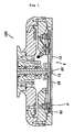
- FIG. 2 is a sectional view showing a carrier head according to one embodiment of the present invention
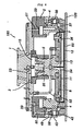
- FIG. 3 is a sectional view of the carrier head according to one embodiment of the present invention, in which a wafer is attached to the carrier head by applying vacuum pressure to the wafer
- FIG. 4 is a sectional view of the carrier head according to one embodiment of the present invention, in which the wafer is pressed in the carrier head
- FIG. 5 is a graph showing a polishing state of a wafer when the wafer is polished by using the carrier head according to one embodiment of the present invention.
- a carrier head 180 according to the present invention is fixed to a carrier driving shaft (not shown) and includes a carrier housing 1, a holder housing 3, a wafer support assembly 6, a retainer ring housing 2, a retainer ring holder 4, a retainer ring 7, a conditioner ring housing 43, and a conditioner 37.
- the carrier housing 1 is fixed to the carrier driving shaft (not shown) in such a manner that it can rotate about a rotational axis, which is substantially perpendicular to a surface of a polishing pad.
- the holder housing 3 is a ring-shaped body installed at a lower center portion of the carrier housing 1.
- the wafer support assembly 6 vertically moves up and down along an inner wall of the holder housing 3 by means of pneumatic pressure.
- the holder housing 3 is formed at a predetermined inner portion thereof with a stepped section for ensuring a lower limit position of the wafer support assembly 6 when the wafer support assembly 6 is moved down due to take thereof.
- the wafer support assembly 6 includes a holder shaft 5 inserted into a hole formed at a center of the holder housing 3 in such a manner that the holder shaft 5 can vertically move up and down, a membrane upper holder 8 installed at a lower portion of the holder shaft 5 in order to support both ends of a membrane 12, and a membrane lower holder 11 installed at a lower portion of the membrane upper holder 8.
- the membrane 12 is fixedly aligned between the membrane upper holder 8 and the membrane lower holder 11 so as to provide a mounting surface for the wafer 60.
- An adjustment chamber 13 is formed between the membrane upper holder 8 and the membrane lower holder 11 in order to adjust internal pressure of a space section formed between the membrane upper holder 8 and the membrane lower holder 11.
- both ends of the membrane 12 are fixed to both ends of the adjustment chamber 13.
- the membrane lower holder 11 is formed at a center thereof with a perforated hole 34.
- pressure is applied to the adjustment chamber 13 while polishing the wafer 60, such pressure is uniformly applied to a rear surface of the membrane 12 through the perforated hole 34, thereby preventing the wafer 60 from sliding on the membrane 12.
- pressure is evenly applied over the whole surface of the wafer 60, so the surface of the wafer 60 can be evenly polished.
- the membrane 12 is made from flexible material and the mounting surface for the wafer 60 is provided at a lower surface of the membrane 12.
- the membrane 12 has a diameter slightly larger than a diameter of the wafer 60.
- the flexible membrane 12 includes rubber or silicon material having elasticity.
- a wafer suction part 41 is formed at a center of the membrane 12. The wafer suction part 41 is connected to a vacuum pipe 35 by passing through the perforated hole 34 formed in the membrane lower holder 11 in order to directly apply vacuum pressure to the wafer 60.
- the wafer suction part 41 is communicated with the vacuum pipe 35 connected to the carrier housing 1 so as to adjust pneumatic pressure such that vacuum pressure and atmospheric pressure are properly maintained. Deionized water is easily supplied through the vacuum pipe 35 so that the vacuum pipe 35 and the carrier head 180 can be easily cleaned.
- the retainer ring housing 2 is attached to a lower end of the carrier housing 1 and is formed at a lower portion thereof with an annular groove to install the retainer ring holder 4 and the conditioner ring housing 43 in the annular groove.
- the retainer ring holder 4 is slidably inserted into the annular groove of the retainer ring housing 2 and a retainer ring chamber 39 communicated with a pressure pipe 51 is formed between the retainer ring holder 4 and the retainer ring housing 2.
- the retainer ring 7 is fixed to the retainer ring holder 4 connected to the wafer support assembly 6 by means of a flexer 14, which prevents impurities from penetrating into the carrier head 180.
- the retainer ring 7 can be moved up and down regardless of the vertical movement of the wafer support assembly 6 by controlling pressure of the retainer ring chamber 39 connected, to the pressure pipe 51.
- the retainer ring 7 is made from hard plastic or ceramic material and has an annular shape having a flat bottom surface 40.
- the conditioner ring housing 43 is fixedly attached to an outer portion of the retainer ring housing 2 and is formed at a lower portion thereof with an annular recess to which a ring tube clamp 49 and a conditioner ring tube 42 are secured.
- a conditioner ring chamber 38 communicated with a pressure pipe 50 is formed in a space section formed in the conditioner ring housing 43.
- vacuum pressure is applied to the retainer ring chamber 39 so as to move up the retainer ring 7, and at the same time, vacuum pressure is also applied to the vacuum pipe 35, thereby attracting the wafer 60.
- pressure is applied to the conditioner chamber 38 to perform conditioning work for the polishing pad 120, so the conditioner tube 42 made from elastic material is expanded, and at the same time, the conditioner 37 is moved down, so that the conditioning work can be carried out with respect to the polishing pad during the polishing process or after the polishing process.
- the wafer 60 is attached to the wafer carrier 180 by directly applying vacuum pressure to the wafer 60, so it is possible to check whether or not the wafer 60 is properly accommodated on the carrier head 180 at proper pressure without requiring an additional device for detecting the wafer 60. If the wafer 60 is dropped from the carrier head 180 or positioned in a wrong place of the carrier head 180, the wafer status may be easily recognized by detecting variation of vacuum pressure in the vacuum pipes installed passing through the carrier head 180 without using an additional device. That is, when the wafer 60 is dropped from the carrier head 180, pressure variation is transmitted into a pressure adjusting unit (not shown) connected to the vacuum pipe 35 and installed at an exterior of the carrier head 180. Thus, the pressure adjusting unit may measure the pressure variation, thereby stopping the polishing process if it is determined that the wafer 60 is dropped from the carrier head 180.
- a pressure adjusting unit may measure the pressure variation, thereby stopping the polishing process if it is determined that the wafer 60 is dropped from the carrier head 180.
- the carrier head of the chemical mechanical polishing apparatus it is possible to install an additional sensing device in the polishing pad 120 for detecting the wafer 60 when the wafer 60 deviates from its position beyond the retainer ring 7 while the polishing process is being carried out through an interaction between the carrier head 180 and the polishing pad 120.
- residual slurry remains on the polishing pad 120 after the chemical mechanical polishing process has been carried out.
- Such residual slurry may directly penetrate into a vacuum line when the wafer 60 is lifted up by means of the carrier head 180 or may adhere to the carrier head 180 after the chemical mechanical polishing process has been finished.
- Such slurry remaining in the vacuum line for a long period of time may be hardened in the vacuum line so that fluid cannot smoothly flow through the vacuum line.
- slurry adhering to the carrier head 180 may cause scratch on the surface of the wafer 60 during the chemical mechanical polishing process or increase friction when internal parts of the carrier head 180 are moved, thereby disturbing the movement of the internal parts.
- deionized water is intermittently fed through the vacuum pipe 35 before or after the chemical mechanical process, thereby cleaning the vacuum line.
- the wafer 60 has been polished by using the carrier head 180.
- the whole surface of the wafer 60 is uniformly polished with a uniform thickness as represented by the graph shown in FIG. 5 .
- the carrier head of the chemical mechanical apparatus attracts the wafer by directly applying vacuum pressure to the wafer, so a suction error or suction fault is reduced in relation to the wafer.
- the present invention can easily check whether or not the wafer is properly accommodated on the mounting surface of the flexible membrane at proper vacuum pressure, thereby improving reliability of the chemical mechanical polishing process while achieving superior polishing quality for the wafer.
Landscapes
- Engineering & Computer Science (AREA)
- Mechanical Engineering (AREA)
- Finish Polishing, Edge Sharpening, And Grinding By Specific Grinding Devices (AREA)
- Mechanical Treatment Of Semiconductor (AREA)
- Electrical Discharge Machining, Electrochemical Machining, And Combined Machining (AREA)
Claims (5)
- Trägerkopf für ein chemisch-mechanisches Poliergerät bzw. ein Gerät zum mechanischen Polieren mit Hilfe von Chemikalien mit:einem Trägergehäuse (1), das durch bzw. über einen Trägerantriebsschaft angetrieben wird;einem Haltergehäuse (3), das an einem unteren zentralen Abschnitt des Trägergehäuses (1) installiert ist und eine Ringform aufweist;einer Waferträgeranordnung (6), die sich vertikal entlang einer inneren Wand des Haltergehäuses (3) nach oben und unten bewegt; undeiner Montage- bzw. Befestigungskammer (10), die es ermöglicht, die Waferträgeranordnung (6) gleitend entlang der inneren Wand des Haltergehäuses (3) auf und ab zu bewegen, und die in einem Zentrum des Haltergehäuses (3) ausgebildet ist, wobei die Waferträgeranordnung (6) eine Einstellungs- bzw. Anpassungskammer (13), die mit Druck beaufschlagt wird, und eine Membran (12), die in einem Zentrum hiervon mit einem Loch ausgebildet ist, aufweist, wobei mit Druck beaufschlagtes Fluid in die Einstellungs- bzw. Anpassungskammer (13) eingeführt wird, während ein Poliervorgang ausgeführt wird, so dass die Membran (12) nach außen expandiert wird, wodurch eine Kraft auf einen vorbestimmten Abschnitt einer rückwärtigen Oberfläche eines Wafers ausgeübt wird;einer Saugeinheit (41), die in einem Zentrum der Membran (12) ausgebildet ist, so dass die Saugeinheit (41) mit einem Vakuumrohr (35), das durch die Einstellungs- bzw. Anpassungskammer (13) hindurch bzw. an ihr vorbei läuft, verbunden ist, undeinem Rückhaltering (7), der an einem äußeren Abschnitt der Waferträgereinheit (6) derart installiert ist, dass der Rückhaltering (7) vertikal senkrecht auf eine untere Oberfläche der Waferträgeranordnung (6) bewegbar ist.
- Trägerkopf nach Anspruch 1, bei dem die Waferträgereinheit (6) einen in ein Loch, das in einem Zentrum des Haltergehäuses (3) ausgebildet ist, eingefügten und in dem Loch vertikal bewegbaren Halterschaft (5), einen an einem unteren Abschnitt des Halterschafts (5) angebrachten oberen Membranhalter (8) und einen an einem unteren Abschnitt des oberen Membranhalters (8) positionierten unteren Membranhalter (11) aufweist, wobei die Membran (12) in Ausrichtung zwischen dem oberen Membranhalter (8) und dem unteren Membranhalter (11) derart befestigt ist, dass eine Befestigungs- bzw. Montageoberfläche für den Wafer (60) bereitgestellt wird.
- Trägerkopf nach Anspruch 1, der ferner einen Conditioner bzw. eine Anpassungsvorrichtung (37) aufweist, der bzw. die an einem äußeren Abschnitt eines Rückhalteringgehäuses (2) derart angebracht ist, dass die Anpassungsvorrichtung vertikal senkrecht auf die untere Oberfläche der Waferträgeranordnung (6) bewegbar ist.
- Trägerkopf nach Anspruch 1, der ferner ein Reinigungsgerät zur Beaufschlagung des Vakuumrohrs (35) mit Reinigungslösung aufweist.
- Trägerkopf nach Anspruch 1, der ferner ein Vakuumdruckmesseinheit aufweist, die mit dem Vakuumrohr (35) zur Messung des Vakuumdrucks in dem Vakuumrohr (35) verbunden ist.
Applications Claiming Priority (2)
| Application Number | Priority Date | Filing Date | Title |
|---|---|---|---|
| KR10-2001-0031788A KR100470227B1 (ko) | 2001-06-07 | 2001-06-07 | 화학기계적 연마장치의 캐리어 헤드 |
| PCT/KR2002/002176 WO2004075275A1 (en) | 2001-06-07 | 2002-11-21 | Carrier head for chemical mechanical polishing apparatus |
Publications (3)
| Publication Number | Publication Date |
|---|---|
| EP1568074A1 EP1568074A1 (de) | 2005-08-31 |
| EP1568074A4 EP1568074A4 (de) | 2007-01-03 |
| EP1568074B1 true EP1568074B1 (de) | 2008-10-15 |
Family
ID=33422235
Family Applications (1)
| Application Number | Title | Priority Date | Filing Date |
|---|---|---|---|
| EP02788980A Expired - Lifetime EP1568074B1 (de) | 2001-06-07 | 2002-11-21 | Trägerkopf für chemisch-mechanische poliervorrichtung |
Country Status (9)
| Country | Link |
|---|---|
| US (1) | US7121934B2 (de) |
| EP (1) | EP1568074B1 (de) |
| JP (1) | JP2006507691A (de) |
| KR (1) | KR100470227B1 (de) |
| CN (1) | CN100390942C (de) |
| AT (1) | ATE411612T1 (de) |
| AU (1) | AU2002353628A1 (de) |
| DE (1) | DE60229449D1 (de) |
| WO (1) | WO2004075275A1 (de) |
Families Citing this family (26)
| Publication number | Priority date | Publication date | Assignee | Title |
|---|---|---|---|---|
| WO2006115453A1 (en) | 2005-04-25 | 2006-11-02 | Smoltek Ab | Controlled growth of a nanostructure on a substrate, and electron emission devices based on the same |
| KR100647041B1 (ko) * | 2005-06-17 | 2006-11-23 | 두산디앤디 주식회사 | 영역분할 연마 프로파일의 경계부 이상연마 제어기능을갖는 화학기계적 연마장치용 캐리어 헤드 |
| US7777291B2 (en) | 2005-08-26 | 2010-08-17 | Smoltek Ab | Integrated circuits having interconnects and heat dissipators based on nanostructures |
| US7364496B2 (en) * | 2006-03-03 | 2008-04-29 | Inopla Inc. | Polishing head for polishing semiconductor wafers |
| US7654888B2 (en) | 2006-11-22 | 2010-02-02 | Applied Materials, Inc. | Carrier head with retaining ring and carrier ring |
| US7699688B2 (en) | 2006-11-22 | 2010-04-20 | Applied Materials, Inc. | Carrier ring for carrier head |
| KR101487346B1 (ko) | 2007-09-12 | 2015-01-28 | 스몰텍 에이비 | 인접 층들을 나노구조들과 연결하고 결합하는 방법 |
| JP5464820B2 (ja) * | 2007-10-29 | 2014-04-09 | 株式会社荏原製作所 | 研磨装置 |
| JP5474835B2 (ja) | 2008-02-25 | 2014-04-16 | スモルテック アーベー | ナノ構造処理のための導電性補助層の形成及び選択的除去 |
| JP5392483B2 (ja) * | 2009-08-31 | 2014-01-22 | 不二越機械工業株式会社 | 研磨装置 |
| US9233452B2 (en) * | 2012-10-29 | 2016-01-12 | Wayne O. Duescher | Vacuum-grooved membrane abrasive polishing wafer workholder |
| US10532441B2 (en) * | 2012-11-30 | 2020-01-14 | Applied Materials, Inc. | Three-zone carrier head and flexible membrane |
| KR101516989B1 (ko) * | 2013-08-12 | 2015-04-30 | 주식회사 케이씨텍 | 압력 감시 정확성이 향상된 화학 기계적 연마 장치 |
| KR101679131B1 (ko) * | 2014-12-29 | 2016-11-23 | 주식회사 엘지실트론 | 웨이퍼 연마장치 및 그 연마방법 |
| KR102459834B1 (ko) * | 2017-11-22 | 2022-10-28 | 주식회사 케이씨텍 | 캐리어 및 이를 포함하는 화학 기계적 연마 장치 |
| CN108145586B (zh) * | 2018-01-03 | 2019-10-11 | 京东方科技集团股份有限公司 | 抛光设备及抛光方法 |
| KR102560114B1 (ko) * | 2018-08-06 | 2023-07-27 | 어플라이드 머티어리얼스, 인코포레이티드 | 비접촉 세정 모듈 |
| KR102747945B1 (ko) * | 2019-02-28 | 2024-12-31 | 어플라이드 머티어리얼스, 인코포레이티드 | 화학적 기계적 연마 캐리어 헤드를 위한 리테이너 |
| CN110142689B (zh) * | 2019-04-17 | 2021-09-14 | 杭州众硅电子科技有限公司 | 一种晶圆装载支架、晶圆装载系统及晶圆装片方法 |
| JP7536601B2 (ja) * | 2020-11-04 | 2024-08-20 | 株式会社荏原製作所 | 研磨ヘッドおよび研磨装置 |
| US11660721B2 (en) * | 2021-02-18 | 2023-05-30 | Applied Materials, Inc. | Dual loading retaining ring |
| CN115106871A (zh) * | 2022-08-29 | 2022-09-27 | 成都中科卓尔智能科技集团有限公司 | 一种半导体材料表面缺陷柔性高精度修复装置及工艺 |
| CN115741250A (zh) * | 2022-12-08 | 2023-03-07 | 华海清科股份有限公司 | 一种化学机械抛光方法 |
| JP2025136592A (ja) * | 2024-03-07 | 2025-09-19 | 株式会社荏原製作所 | 基板研磨装置、基板処理装置、基板研磨方法、およびプログラム |
| CN117983902B (zh) * | 2024-04-07 | 2024-06-04 | 常州江泉传动科技有限公司 | 一种齿轮减速机生产用行星齿轮加工装置 |
| CN119077606B (zh) * | 2024-09-26 | 2026-02-06 | 华海清科股份有限公司 | 用于晶圆加工的承载头及化学机械抛光设备 |
Family Cites Families (30)
| Publication number | Priority date | Publication date | Assignee | Title |
|---|---|---|---|---|
| GB8829089D0 (en) * | 1988-12-13 | 1989-01-25 | Coopers Animal Health | Intra ruminal device |
| JP3370112B2 (ja) * | 1992-10-12 | 2003-01-27 | 不二越機械工業株式会社 | ウエハーの研磨装置 |
| US5681215A (en) | 1995-10-27 | 1997-10-28 | Applied Materials, Inc. | Carrier head design for a chemical mechanical polishing apparatus |
| US5643061A (en) * | 1995-07-20 | 1997-07-01 | Integrated Process Equipment Corporation | Pneumatic polishing head for CMP apparatus |
| US5762544A (en) * | 1995-10-27 | 1998-06-09 | Applied Materials, Inc. | Carrier head design for a chemical mechanical polishing apparatus |
| US6036587A (en) * | 1996-10-10 | 2000-03-14 | Applied Materials, Inc. | Carrier head with layer of conformable material for a chemical mechanical polishing system |
| JP3724911B2 (ja) * | 1997-04-08 | 2005-12-07 | 株式会社荏原製作所 | ポリッシング装置 |
| US5957751A (en) * | 1997-05-23 | 1999-09-28 | Applied Materials, Inc. | Carrier head with a substrate detection mechanism for a chemical mechanical polishing system |
| US6398621B1 (en) * | 1997-05-23 | 2002-06-04 | Applied Materials, Inc. | Carrier head with a substrate sensor |
| US5964653A (en) * | 1997-07-11 | 1999-10-12 | Applied Materials, Inc. | Carrier head with a flexible membrane for a chemical mechanical polishing system |
| US5916015A (en) * | 1997-07-25 | 1999-06-29 | Speedfam Corporation | Wafer carrier for semiconductor wafer polishing machine |
| US5993302A (en) * | 1997-12-31 | 1999-11-30 | Applied Materials, Inc. | Carrier head with a removable retaining ring for a chemical mechanical polishing apparatus |
| US5961169A (en) * | 1998-07-27 | 1999-10-05 | Strasbaugh | Apparatus for sensing the presence of a wafer |
| US6210255B1 (en) * | 1998-09-08 | 2001-04-03 | Applied Materials, Inc. | Carrier head for chemical mechanical polishing a substrate |
| US6162116A (en) | 1999-01-23 | 2000-12-19 | Applied Materials, Inc. | Carrier head for chemical mechanical polishing |
| US6231428B1 (en) * | 1999-03-03 | 2001-05-15 | Mitsubishi Materials Corporation | Chemical mechanical polishing head assembly having floating wafer carrier and retaining ring |
| US6224472B1 (en) * | 1999-06-24 | 2001-05-01 | Samsung Austin Semiconductor, L.P. | Retaining ring for chemical mechanical polishing |
| US6358121B1 (en) * | 1999-07-09 | 2002-03-19 | Applied Materials, Inc. | Carrier head with a flexible membrane and an edge load ring |
| US6206768B1 (en) * | 1999-07-29 | 2001-03-27 | Chartered Semiconductor Manufacturing, Ltd. | Adjustable and extended guide rings |
| KR20010030213A (ko) * | 1999-09-02 | 2001-04-16 | 아끼모토 유미 | 연마 헤드, 이것을 이용한 연마 장치, 및 연마 상태 검출방법 |
| SG90746A1 (en) * | 1999-10-15 | 2002-08-20 | Ebara Corp | Apparatus and method for polishing workpiece |
| WO2001087541A2 (en) * | 2000-05-12 | 2001-11-22 | Multi-Planar Technologies, Inc. | Pneumatic diaphragm head having an independent retaining ring and multi-region pressure control, and method to use the same |
| US6558232B1 (en) * | 2000-05-12 | 2003-05-06 | Multi-Planar Technologies, Inc. | System and method for CMP having multi-pressure zone loading for improved edge and annular zone material removal control |
| US6540590B1 (en) * | 2000-08-31 | 2003-04-01 | Multi-Planar Technologies, Inc. | Chemical mechanical polishing apparatus and method having a rotating retaining ring |
| JP2002187060A (ja) * | 2000-10-11 | 2002-07-02 | Ebara Corp | 基板保持装置、ポリッシング装置、及び研磨方法 |
| KR100423909B1 (ko) * | 2000-11-23 | 2004-03-24 | 삼성전자주식회사 | 화학적 기계적 평탄화 기계의 폴리싱 헤드 및 그것을이용한 폴리싱방법 |
| US6652362B2 (en) * | 2000-11-23 | 2003-11-25 | Samsung Electronics Co., Ltd. | Apparatus for polishing a semiconductor wafer and method therefor |
| DE10062496B4 (de) * | 2000-12-14 | 2005-03-17 | Peter Wolters Cmp - Systeme Gmbh & Co. Kg | Halter für flache Werkstücke, insbesondere Halbleiterwafer |
| JP3922887B2 (ja) * | 2001-03-16 | 2007-05-30 | 株式会社荏原製作所 | ドレッサ及びポリッシング装置 |
| US6893327B2 (en) * | 2001-06-04 | 2005-05-17 | Multi Planar Technologies, Inc. | Chemical mechanical polishing apparatus and method having a retaining ring with a contoured surface |
-
2001
- 2001-06-07 KR KR10-2001-0031788A patent/KR100470227B1/ko not_active Expired - Fee Related
-
2002
- 2002-11-21 CN CNB028300696A patent/CN100390942C/zh not_active Expired - Fee Related
- 2002-11-21 WO PCT/KR2002/002176 patent/WO2004075275A1/en not_active Ceased
- 2002-11-21 DE DE60229449T patent/DE60229449D1/de not_active Expired - Fee Related
- 2002-11-21 AU AU2002353628A patent/AU2002353628A1/en not_active Abandoned
- 2002-11-21 JP JP2004568513A patent/JP2006507691A/ja not_active Ceased
- 2002-11-21 EP EP02788980A patent/EP1568074B1/de not_active Expired - Lifetime
- 2002-11-21 AT AT02788980T patent/ATE411612T1/de not_active IP Right Cessation
-
2005
- 2005-05-18 US US11/133,148 patent/US7121934B2/en not_active Expired - Lifetime
Also Published As
| Publication number | Publication date |
|---|---|
| CN1723546A (zh) | 2006-01-18 |
| US7121934B2 (en) | 2006-10-17 |
| KR100470227B1 (ko) | 2005-02-05 |
| JP2006507691A (ja) | 2006-03-02 |
| WO2004075275A1 (en) | 2004-09-02 |
| DE60229449D1 (de) | 2008-11-27 |
| EP1568074A1 (de) | 2005-08-31 |
| KR20020094079A (ko) | 2002-12-18 |
| CN100390942C (zh) | 2008-05-28 |
| US20050272355A1 (en) | 2005-12-08 |
| EP1568074A4 (de) | 2007-01-03 |
| AU2002353628A1 (en) | 2004-09-09 |
| ATE411612T1 (de) | 2008-10-15 |
Similar Documents
| Publication | Publication Date | Title |
|---|---|---|
| EP1568074B1 (de) | Trägerkopf für chemisch-mechanische poliervorrichtung | |
| KR100939555B1 (ko) | 기판 유지 장치 | |
| US5899801A (en) | Method and apparatus for removing a substrate from a polishing pad in a chemical mechanical polishing system | |
| US6645044B2 (en) | Method of chemical mechanical polishing with controllable pressure and loading area | |
| US5624299A (en) | Chemical mechanical polishing apparatus with improved carrier and method of use | |
| US6210255B1 (en) | Carrier head for chemical mechanical polishing a substrate | |
| JP4212776B2 (ja) | 化学機械的研磨ヘッド | |
| US8430716B2 (en) | Polishing method and polishing apparatus | |
| US6494774B1 (en) | Carrier head with pressure transfer mechanism | |
| US6358121B1 (en) | Carrier head with a flexible membrane and an edge load ring | |
| KR19980042123A (ko) | 화학 기계적 폴리싱 장치용 가요성 박막을 갖는 캐리어 헤드 | |
| WO2000013851A1 (en) | A carrier head for chemical mechanical polishing a substrate | |
| WO2000021714A1 (en) | A carrier head with a flexible membrane for chemical mechanical polishing | |
| US20230356353A1 (en) | Carrier Head Membrane With Regions of Different Roughness | |
| KR100335569B1 (ko) | 화학적 기계적 연마장치의 연마헤드 | |
| US7101271B2 (en) | Polishing head and chemical mechanical polishing apparatus | |
| KR100349216B1 (ko) | 화학적 기계적 연마장치의 연마헤드 | |
| JP2004297029A (ja) | 基板保持装置及び研磨装置 | |
| KR100387385B1 (ko) | 부상 웨이퍼 유지 링을 구비한 화학적 기계적 연마 헤드및 다중 구역 연마 압력 제어부를 갖춘 웨이퍼 캐리어 | |
| KR100470228B1 (ko) | 화학기계적 연마장치의 캐리어 헤드 | |
| JPH08150558A (ja) | 研磨装置 | |
| US20040192179A1 (en) | Dual-bulge flexure ring for CMP head | |
| KR20030055840A (ko) | 화학적 기계적 연마장치의 연마헤드 |
Legal Events
| Date | Code | Title | Description |
|---|---|---|---|
| PUAI | Public reference made under article 153(3) epc to a published international application that has entered the european phase |
Free format text: ORIGINAL CODE: 0009012 |
|
| 17P | Request for examination filed |
Effective date: 20050609 |
|
| AK | Designated contracting states |
Kind code of ref document: A1 Designated state(s): AT BE BG CH CY CZ DE DK EE ES FI FR GB GR IE IT LI LU MC NL PT SE SK TR |
|
| AX | Request for extension of the european patent |
Extension state: AL LT LV MK RO SI |
|
| RAP1 | Party data changed (applicant data changed or rights of an application transferred) |
Owner name: DOOSAN DND CO., LTD. |
|
| DAX | Request for extension of the european patent (deleted) | ||
| A4 | Supplementary search report drawn up and despatched |
Effective date: 20061206 |
|
| RIC1 | Information provided on ipc code assigned before grant |
Ipc: H01L 21/302 20060101AFI20040909BHEP Ipc: B24B 37/04 20060101ALI20061130BHEP Ipc: B24B 41/06 20060101ALI20061130BHEP |
|
| 17Q | First examination report despatched |
Effective date: 20070529 |
|
| GRAP | Despatch of communication of intention to grant a patent |
Free format text: ORIGINAL CODE: EPIDOSNIGR1 |
|
| RAP1 | Party data changed (applicant data changed or rights of an application transferred) |
Owner name: DOOSAN MECATEC CO., LTD. |
|
| GRAS | Grant fee paid |
Free format text: ORIGINAL CODE: EPIDOSNIGR3 |
|
| GRAA | (expected) grant |
Free format text: ORIGINAL CODE: 0009210 |
|
| AK | Designated contracting states |
Kind code of ref document: B1 Designated state(s): AT BE BG CH CY CZ DE DK EE ES FI FR GB GR IE IT LI LU MC NL PT SE SK TR |
|
| REG | Reference to a national code |
Ref country code: CH Ref legal event code: EP Ref country code: GB Ref legal event code: FG4D |
|
| REG | Reference to a national code |
Ref country code: IE Ref legal event code: FG4D |
|
| REF | Corresponds to: |
Ref document number: 60229449 Country of ref document: DE Date of ref document: 20081127 Kind code of ref document: P |
|
| PGFP | Annual fee paid to national office [announced via postgrant information from national office to epo] |
Ref country code: DE Payment date: 20081117 Year of fee payment: 7 |
|
| NLV1 | Nl: lapsed or annulled due to failure to fulfill the requirements of art. 29p and 29m of the patents act | ||
| PG25 | Lapsed in a contracting state [announced via postgrant information from national office to epo] |
Ref country code: AT Free format text: LAPSE BECAUSE OF FAILURE TO SUBMIT A TRANSLATION OF THE DESCRIPTION OR TO PAY THE FEE WITHIN THE PRESCRIBED TIME-LIMIT Effective date: 20081015 Ref country code: BG Free format text: LAPSE BECAUSE OF FAILURE TO SUBMIT A TRANSLATION OF THE DESCRIPTION OR TO PAY THE FEE WITHIN THE PRESCRIBED TIME-LIMIT Effective date: 20090115 Ref country code: ES Free format text: LAPSE BECAUSE OF FAILURE TO SUBMIT A TRANSLATION OF THE DESCRIPTION OR TO PAY THE FEE WITHIN THE PRESCRIBED TIME-LIMIT Effective date: 20090126 |
|
| PGFP | Annual fee paid to national office [announced via postgrant information from national office to epo] |
Ref country code: FR Payment date: 20081118 Year of fee payment: 7 |
|
| PG25 | Lapsed in a contracting state [announced via postgrant information from national office to epo] |
Ref country code: FI Free format text: LAPSE BECAUSE OF FAILURE TO SUBMIT A TRANSLATION OF THE DESCRIPTION OR TO PAY THE FEE WITHIN THE PRESCRIBED TIME-LIMIT Effective date: 20081015 Ref country code: NL Free format text: LAPSE BECAUSE OF FAILURE TO SUBMIT A TRANSLATION OF THE DESCRIPTION OR TO PAY THE FEE WITHIN THE PRESCRIBED TIME-LIMIT Effective date: 20081015 Ref country code: PT Free format text: LAPSE BECAUSE OF FAILURE TO SUBMIT A TRANSLATION OF THE DESCRIPTION OR TO PAY THE FEE WITHIN THE PRESCRIBED TIME-LIMIT Effective date: 20090316 |
|
| PG25 | Lapsed in a contracting state [announced via postgrant information from national office to epo] |
Ref country code: MC Free format text: LAPSE BECAUSE OF NON-PAYMENT OF DUE FEES Effective date: 20081130 |
|
| REG | Reference to a national code |
Ref country code: CH Ref legal event code: PL |
|
| PG25 | Lapsed in a contracting state [announced via postgrant information from national office to epo] |
Ref country code: DK Free format text: LAPSE BECAUSE OF FAILURE TO SUBMIT A TRANSLATION OF THE DESCRIPTION OR TO PAY THE FEE WITHIN THE PRESCRIBED TIME-LIMIT Effective date: 20081015 Ref country code: BE Free format text: LAPSE BECAUSE OF FAILURE TO SUBMIT A TRANSLATION OF THE DESCRIPTION OR TO PAY THE FEE WITHIN THE PRESCRIBED TIME-LIMIT Effective date: 20081015 Ref country code: EE Free format text: LAPSE BECAUSE OF FAILURE TO SUBMIT A TRANSLATION OF THE DESCRIPTION OR TO PAY THE FEE WITHIN THE PRESCRIBED TIME-LIMIT Effective date: 20081015 |
|
| REG | Reference to a national code |
Ref country code: IE Ref legal event code: MM4A |
|
| PLBE | No opposition filed within time limit |
Free format text: ORIGINAL CODE: 0009261 |
|
| STAA | Information on the status of an ep patent application or granted ep patent |
Free format text: STATUS: NO OPPOSITION FILED WITHIN TIME LIMIT |
|
| PG25 | Lapsed in a contracting state [announced via postgrant information from national office to epo] |
Ref country code: SE Free format text: LAPSE BECAUSE OF FAILURE TO SUBMIT A TRANSLATION OF THE DESCRIPTION OR TO PAY THE FEE WITHIN THE PRESCRIBED TIME-LIMIT Effective date: 20090115 Ref country code: CZ Free format text: LAPSE BECAUSE OF FAILURE TO SUBMIT A TRANSLATION OF THE DESCRIPTION OR TO PAY THE FEE WITHIN THE PRESCRIBED TIME-LIMIT Effective date: 20081015 Ref country code: IT Free format text: LAPSE BECAUSE OF FAILURE TO SUBMIT A TRANSLATION OF THE DESCRIPTION OR TO PAY THE FEE WITHIN THE PRESCRIBED TIME-LIMIT Effective date: 20081015 |
|
| 26N | No opposition filed |
Effective date: 20090716 |
|
| GBPC | Gb: european patent ceased through non-payment of renewal fee |
Effective date: 20090115 |
|
| PG25 | Lapsed in a contracting state [announced via postgrant information from national office to epo] |
Ref country code: SK Free format text: LAPSE BECAUSE OF FAILURE TO SUBMIT A TRANSLATION OF THE DESCRIPTION OR TO PAY THE FEE WITHIN THE PRESCRIBED TIME-LIMIT Effective date: 20081015 |
|
| PG25 | Lapsed in a contracting state [announced via postgrant information from national office to epo] |
Ref country code: LI Free format text: LAPSE BECAUSE OF NON-PAYMENT OF DUE FEES Effective date: 20081130 Ref country code: IE Free format text: LAPSE BECAUSE OF NON-PAYMENT OF DUE FEES Effective date: 20081121 Ref country code: CH Free format text: LAPSE BECAUSE OF NON-PAYMENT OF DUE FEES Effective date: 20081130 |
|
| PG25 | Lapsed in a contracting state [announced via postgrant information from national office to epo] |
Ref country code: GB Free format text: LAPSE BECAUSE OF NON-PAYMENT OF DUE FEES Effective date: 20090115 |
|
| PG25 | Lapsed in a contracting state [announced via postgrant information from national office to epo] |
Ref country code: LU Free format text: LAPSE BECAUSE OF NON-PAYMENT OF DUE FEES Effective date: 20081121 Ref country code: CY Free format text: LAPSE BECAUSE OF FAILURE TO SUBMIT A TRANSLATION OF THE DESCRIPTION OR TO PAY THE FEE WITHIN THE PRESCRIBED TIME-LIMIT Effective date: 20081015 |
|
| REG | Reference to a national code |
Ref country code: FR Ref legal event code: ST Effective date: 20100730 |
|
| PG25 | Lapsed in a contracting state [announced via postgrant information from national office to epo] |
Ref country code: TR Free format text: LAPSE BECAUSE OF FAILURE TO SUBMIT A TRANSLATION OF THE DESCRIPTION OR TO PAY THE FEE WITHIN THE PRESCRIBED TIME-LIMIT Effective date: 20081015 |
|
| PG25 | Lapsed in a contracting state [announced via postgrant information from national office to epo] |
Ref country code: FR Free format text: LAPSE BECAUSE OF NON-PAYMENT OF DUE FEES Effective date: 20091130 Ref country code: GR Free format text: LAPSE BECAUSE OF FAILURE TO SUBMIT A TRANSLATION OF THE DESCRIPTION OR TO PAY THE FEE WITHIN THE PRESCRIBED TIME-LIMIT Effective date: 20090116 |
|
| PG25 | Lapsed in a contracting state [announced via postgrant information from national office to epo] |
Ref country code: DE Free format text: LAPSE BECAUSE OF NON-PAYMENT OF DUE FEES Effective date: 20100601 |