EP1567915B1 - Pattern forming materials and pattern formation method using the materials - Google Patents
Pattern forming materials and pattern formation method using the materials Download PDFInfo
- Publication number
- EP1567915B1 EP1567915B1 EP03754229A EP03754229A EP1567915B1 EP 1567915 B1 EP1567915 B1 EP 1567915B1 EP 03754229 A EP03754229 A EP 03754229A EP 03754229 A EP03754229 A EP 03754229A EP 1567915 B1 EP1567915 B1 EP 1567915B1
- Authority
- EP
- European Patent Office
- Prior art keywords
- light
- layer
- sensitive material
- material layer
- thermal sensitive
- Prior art date
- Legal status (The legal status is an assumption and is not a legal conclusion. Google has not performed a legal analysis and makes no representation as to the accuracy of the status listed.)
- Expired - Lifetime
Links
- 239000000463 material Substances 0.000 title claims abstract description 136
- 238000000034 method Methods 0.000 title claims description 52
- 230000007261 regionalization Effects 0.000 title description 4
- 239000000758 substrate Substances 0.000 claims abstract description 52
- 229920002120 photoresistant polymer Polymers 0.000 claims abstract description 26
- 239000010410 layer Substances 0.000 claims description 206
- 230000004913 activation Effects 0.000 claims description 62
- 239000011241 protective layer Substances 0.000 claims description 17
- 229910001215 Te alloy Inorganic materials 0.000 claims description 3
- 238000006243 chemical reaction Methods 0.000 description 13
- VYPSYNLAJGMNEJ-UHFFFAOYSA-N Silicium dioxide Chemical compound O=[Si]=O VYPSYNLAJGMNEJ-UHFFFAOYSA-N 0.000 description 10
- 238000000059 patterning Methods 0.000 description 8
- 239000000243 solution Substances 0.000 description 8
- 230000003287 optical effect Effects 0.000 description 7
- 150000004770 chalcogenides Chemical class 0.000 description 6
- 238000009826 distribution Methods 0.000 description 6
- 238000011161 development Methods 0.000 description 5
- 230000018109 developmental process Effects 0.000 description 5
- 239000000377 silicon dioxide Substances 0.000 description 5
- KWYUFKZDYYNOTN-UHFFFAOYSA-M Potassium hydroxide Chemical compound [OH-].[K+] KWYUFKZDYYNOTN-UHFFFAOYSA-M 0.000 description 4
- 229910052681 coesite Inorganic materials 0.000 description 4
- 229910052906 cristobalite Inorganic materials 0.000 description 4
- 230000008020 evaporation Effects 0.000 description 4
- 238000001704 evaporation Methods 0.000 description 4
- 238000004519 manufacturing process Methods 0.000 description 4
- 238000012545 processing Methods 0.000 description 4
- 229910052682 stishovite Inorganic materials 0.000 description 4
- 229910052905 tridymite Inorganic materials 0.000 description 4
- 229910052782 aluminium Inorganic materials 0.000 description 3
- XAGFODPZIPBFFR-UHFFFAOYSA-N aluminium Chemical compound [Al] XAGFODPZIPBFFR-UHFFFAOYSA-N 0.000 description 3
- 238000010894 electron beam technology Methods 0.000 description 3
- 239000011521 glass Substances 0.000 description 3
- 238000001459 lithography Methods 0.000 description 3
- 238000000206 photolithography Methods 0.000 description 3
- 239000004065 semiconductor Substances 0.000 description 3
- 229910052715 tantalum Inorganic materials 0.000 description 3
- GUVRBAGPIYLISA-UHFFFAOYSA-N tantalum atom Chemical compound [Ta] GUVRBAGPIYLISA-UHFFFAOYSA-N 0.000 description 3
- KRHYYFGTRYWZRS-UHFFFAOYSA-N Fluorane Chemical compound F KRHYYFGTRYWZRS-UHFFFAOYSA-N 0.000 description 2
- -1 ZnS· SiO2 Chemical class 0.000 description 2
- 238000007796 conventional method Methods 0.000 description 2
- 238000001312 dry etching Methods 0.000 description 2
- 238000000609 electron-beam lithography Methods 0.000 description 2
- 238000005516 engineering process Methods 0.000 description 2
- 238000010438 heat treatment Methods 0.000 description 2
- 238000001020 plasma etching Methods 0.000 description 2
- 229920003023 plastic Polymers 0.000 description 2
- 229920005989 resin Polymers 0.000 description 2
- 239000011347 resin Substances 0.000 description 2
- 238000001039 wet etching Methods 0.000 description 2
- 229920000178 Acrylic resin Polymers 0.000 description 1
- 239000004925 Acrylic resin Substances 0.000 description 1
- JBRZTFJDHDCESZ-UHFFFAOYSA-N AsGa Chemical compound [As]#[Ga] JBRZTFJDHDCESZ-UHFFFAOYSA-N 0.000 description 1
- BVKZGUZCCUSVTD-UHFFFAOYSA-L Carbonate Chemical compound [O-]C([O-])=O BVKZGUZCCUSVTD-UHFFFAOYSA-L 0.000 description 1
- MHAJPDPJQMAIIY-UHFFFAOYSA-N Hydrogen peroxide Chemical compound OO MHAJPDPJQMAIIY-UHFFFAOYSA-N 0.000 description 1
- 239000004642 Polyimide Substances 0.000 description 1
- 239000004743 Polypropylene Substances 0.000 description 1
- XUIMIQQOPSSXEZ-UHFFFAOYSA-N Silicon Chemical compound [Si] XUIMIQQOPSSXEZ-UHFFFAOYSA-N 0.000 description 1
- 229910000756 V alloy Inorganic materials 0.000 description 1
- BZHJMEDXRYGGRV-UHFFFAOYSA-N Vinyl chloride Chemical compound ClC=C BZHJMEDXRYGGRV-UHFFFAOYSA-N 0.000 description 1
- 230000001133 acceleration Effects 0.000 description 1
- 239000012670 alkaline solution Substances 0.000 description 1
- 238000004132 cross linking Methods 0.000 description 1
- 230000007547 defect Effects 0.000 description 1
- 239000003989 dielectric material Substances 0.000 description 1
- 238000005265 energy consumption Methods 0.000 description 1
- 238000005530 etching Methods 0.000 description 1
- 230000020169 heat generation Effects 0.000 description 1
- 150000002484 inorganic compounds Chemical class 0.000 description 1
- 229910010272 inorganic material Inorganic materials 0.000 description 1
- GQYHUHYESMUTHG-UHFFFAOYSA-N lithium niobate Chemical compound [Li+].[O-][Nb](=O)=O GQYHUHYESMUTHG-UHFFFAOYSA-N 0.000 description 1
- 238000004377 microelectronic Methods 0.000 description 1
- 238000005459 micromachining Methods 0.000 description 1
- 239000000203 mixture Substances 0.000 description 1
- KDEDDPRZIDYFOB-UHFFFAOYSA-N n-methyl-n-phenylnitramide Chemical compound [O-][N+](=O)N(C)C1=CC=CC=C1 KDEDDPRZIDYFOB-UHFFFAOYSA-N 0.000 description 1
- 150000002894 organic compounds Chemical class 0.000 description 1
- 239000004033 plastic Substances 0.000 description 1
- 229920000515 polycarbonate Polymers 0.000 description 1
- 239000004417 polycarbonate Substances 0.000 description 1
- 229920001721 polyimide Polymers 0.000 description 1
- 229920001155 polypropylene Polymers 0.000 description 1
- 229920005990 polystyrene resin Polymers 0.000 description 1
- 238000011160 research Methods 0.000 description 1
- 229910052710 silicon Inorganic materials 0.000 description 1
- 239000010703 silicon Substances 0.000 description 1
- 238000004544 sputter deposition Methods 0.000 description 1
- 230000008961 swelling Effects 0.000 description 1
Images


Classifications
-
- G—PHYSICS
- G11—INFORMATION STORAGE
- G11B—INFORMATION STORAGE BASED ON RELATIVE MOVEMENT BETWEEN RECORD CARRIER AND TRANSDUCER
- G11B7/00—Recording or reproducing by optical means, e.g. recording using a thermal beam of optical radiation by modifying optical properties or the physical structure, reproducing using an optical beam at lower power by sensing optical properties; Record carriers therefor
- G11B7/24—Record carriers characterised by shape, structure or physical properties, or by the selection of the material
- G11B7/26—Apparatus or processes specially adapted for the manufacture of record carriers
- G11B7/261—Preparing a master, e.g. exposing photoresist, electroforming
-
- B—PERFORMING OPERATIONS; TRANSPORTING
- B41—PRINTING; LINING MACHINES; TYPEWRITERS; STAMPS
- B41M—PRINTING, DUPLICATING, MARKING, OR COPYING PROCESSES; COLOUR PRINTING
- B41M5/00—Duplicating or marking methods; Sheet materials for use therein
- B41M5/26—Thermography ; Marking by high energetic means, e.g. laser otherwise than by burning, and characterised by the material used
- B41M5/40—Thermography ; Marking by high energetic means, e.g. laser otherwise than by burning, and characterised by the material used characterised by the base backcoat, intermediate, or covering layers, e.g. for thermal transfer dye-donor or dye-receiver sheets; Heat, radiation filtering or absorbing means or layers; combined with other image registration layers or compositions; Special originals for reproduction by thermography
- B41M5/46—Thermography ; Marking by high energetic means, e.g. laser otherwise than by burning, and characterised by the material used characterised by the base backcoat, intermediate, or covering layers, e.g. for thermal transfer dye-donor or dye-receiver sheets; Heat, radiation filtering or absorbing means or layers; combined with other image registration layers or compositions; Special originals for reproduction by thermography characterised by the light-to-heat converting means; characterised by the heat or radiation filtering or absorbing means or layers
-
- B—PERFORMING OPERATIONS; TRANSPORTING
- B41—PRINTING; LINING MACHINES; TYPEWRITERS; STAMPS
- B41M—PRINTING, DUPLICATING, MARKING, OR COPYING PROCESSES; COLOUR PRINTING
- B41M5/00—Duplicating or marking methods; Sheet materials for use therein
- B41M5/26—Thermography ; Marking by high energetic means, e.g. laser otherwise than by burning, and characterised by the material used
- B41M5/36—Thermography ; Marking by high energetic means, e.g. laser otherwise than by burning, and characterised by the material used using a polymeric layer, which may be particulate and which is deformed or structurally changed with modification of its' properties, e.g. of its' optical hydrophobic-hydrophilic, solubility or permeability properties
- B41M5/368—Thermography ; Marking by high energetic means, e.g. laser otherwise than by burning, and characterised by the material used using a polymeric layer, which may be particulate and which is deformed or structurally changed with modification of its' properties, e.g. of its' optical hydrophobic-hydrophilic, solubility or permeability properties involving the creation of a soluble/insoluble or hydrophilic/hydrophobic permeability pattern; Peel development
-
- B—PERFORMING OPERATIONS; TRANSPORTING
- B41—PRINTING; LINING MACHINES; TYPEWRITERS; STAMPS
- B41M—PRINTING, DUPLICATING, MARKING, OR COPYING PROCESSES; COLOUR PRINTING
- B41M5/00—Duplicating or marking methods; Sheet materials for use therein
- B41M5/26—Thermography ; Marking by high energetic means, e.g. laser otherwise than by burning, and characterised by the material used
- B41M5/40—Thermography ; Marking by high energetic means, e.g. laser otherwise than by burning, and characterised by the material used characterised by the base backcoat, intermediate, or covering layers, e.g. for thermal transfer dye-donor or dye-receiver sheets; Heat, radiation filtering or absorbing means or layers; combined with other image registration layers or compositions; Special originals for reproduction by thermography
- B41M5/46—Thermography ; Marking by high energetic means, e.g. laser otherwise than by burning, and characterised by the material used characterised by the base backcoat, intermediate, or covering layers, e.g. for thermal transfer dye-donor or dye-receiver sheets; Heat, radiation filtering or absorbing means or layers; combined with other image registration layers or compositions; Special originals for reproduction by thermography characterised by the light-to-heat converting means; characterised by the heat or radiation filtering or absorbing means or layers
- B41M5/465—Infra-red radiation-absorbing materials, e.g. dyes, metals, silicates, C black
Definitions
- the present invention relates to micromachining of a substrate, and more particularly, to a material for use in forming a fine pattern on a substrate and a method of forming a fine pattern using the material.
- Fine patterning methods such as photolithography, using vacuum ultraviolet rays (VUV) or X-rays, which are applied in the manufacture of semiconductor integrated circuits or electronic/electrical parts, including optical discs, has been conducted.
- Fine pattern structures with a line width of 0.1 m can be realized in current situations based on such patterning techniques, and their commercialization is expected in a few years.
- a conventional method of forming a resist pattern in the manufacture of electronic/electrical parts involves activation light irradiation onto a photoresist layer through a predetermined mask pattern and development. Accordingly, the minimal dimensions of the resist pattern is limited, in practice, to be slightly smaller than the wavelength of activation light used, due to diffraction of the activation light.
- the diffraction limit relies on the wavelength of light and the numerical aperture of a lens used. Shorter wavelength of light and greater numerical aperture of a lens are more effective to reduce the diffraction limit. However, since increasing the numerical aperture of the lens has encountered limitations in the current technical status, there are more trends toward using shorter wavelength light to form smaller resist patterns.
- Electron beam lithography ensures much finer pattern processing for a few nanometer pattern dimension compared to photolithography.
- electron beam lithography requires an additional vacuum enclosure, a large electrode, and a high power source for electron acceleration or deflection.
- the use of a high accelerating voltage of tens of kilovolts raises safety concerns.
- Japanese Patent Application No. hei 8-249493 discloses a pattern formation method in which the crystalline state of chalcogenide is thermally changed by laser light irradiation. This fine patterning method is based on variation in etch rate between different crystalline states and ensures patterning to be smaller than the diffraction limit. However, the variation in etch rate depending on crystalline states is not large enough, and the uneven chalcogenide layer leads to varying etch rates even for the same crystalline state.
- chalcogenide layer is etched first at an intercrystalline domain so that a quality fine pattern is not guaranteed.
- chalcogenide which is an essential material of the disclosure, cannot be applied to form a fine pattern for semiconductors. Other problems arise from the change of the chalcogenide.
- a pattern forming material which thermally changes by activation light irradiation and a patterning method using the material are suggested ( Microelectronic Engineering 61-62, 2002, p. 415-421 ).
- a light-to-heat converting material layer made of Ge 2 Sb 2 Te 5 is interposed between a target substrate and a photoresist layer to be patterned and is subjected to activation light irradiation to generate heat.
- the heat generated in the Ge 2 Sb 2 Te 5 layer is transferred to the overlying photoresist layer to induce chemical reactions and form a fine pattern therein.
- a pattern of 100 nm can be formed with this method.
- the disclosed method is regarded to be very economical and offers higher processing precision and finer pattern processing ability compared to the method using chalcogenide.
- the above resist patterning method using the light-to-heat converting material layer has the following limitations.
- the amount of heat transferred from the light-to-heat converting layer to the photoresist layer is not enough to form a desired fine pattern.
- the maximum pattern height that can be obtained with this method is limited to 30 nm when the width of a pattern is designed at 100 nm. In other words, this method cannot be applied to form a high aspect ratio pattern on a substrate.
- the intensity of laser light radiated is increased to generate larger amount of heat or for higher processing rate or greater pattern height, the photoresist layer undesirably evaporates and disappears.
- the present invention provides new pattern forming materials useful for a high aspect ratio fine pattern and a pattern formation method using the materials.
- the present invention provides a method of efficiently forming a high aspect ratio fine pattern in a thermal sensitive material layer formed on a target substrate using heat generated at first and second light-to-heat converting layer formed on both surfaces of the thermal sensitive material layer, via activation light irradiation.
- pattern forming materials comprising: a thermal sensitive material layer formed over a target substrate; a first light-to-heat converting layer formed between the thermal sensitive material layer and the target substrate; and a second light-to-heat converting layer formed on a surface of the thermal sensitive material layer opposite to the first light-to-heat converting layer, the thermal sensitive material layer being interposed between the first and second light-to-heat converting layers.
- both surfaces of the photo and thermal sensitive material layer are efficiently heated by activation light irradiation without evaporation or deformation thereof.
- a resulting fine pattern has a whole shape and a higher aspect ratio.
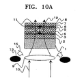
- FIG. 1 illustrates an exemplary structure of pattern forming materials according to the present invention and the principle of forming a fine pattern using the pattern forming materials.
- the pattern forming materials of FIG. 1 include a first light-to-heat converting layer 3, a first thermal buffer layer 4, a photo and thermal sensitive material layer 5, a second thermal buffer layer 6, a second light-to-heat converting layer 7, and a cap layer 8, which are sequentially stacked upon one another, with a substrate protective layer 2 between the first light-to-heat converting layer 3 and a target substrate 1.
- activation light 10 When activation light 10 is radiated onto the pattern forming materials having the above structure via a lens 9, the energy of the activation light 10 is converted into heat 11 by the function of the first and second light-to-heat converting layers 3 and 7. The heat 11 is transferred via the first and second thermal buffer layers 4 and 6 to heat a pattern portion 12 of the photo and thermal sensitive material layer 5 and induce chemical reaction therein.
- the activation light 10 is illustrated as being radiated through the target substrate 1, the activation light 10 may be radiated in a direction opposite to the target substrate 1 if necessary.
- the thickness of each layer is determined to be in a range of 2-200 nm. However, each layer may be formed to be thinner or thicker than the above range depending on a desired pattern size or the material composing the photo and thermal sensitive material layer 5.
- the activation light 10 is not fully absorbed by the first light-to-heat converting layer 3, and a large portion of the activation light 10 transmits the first light-to-heat converting layer 3.
- the transmitted portion of the activation light 10 is absorbed and converted into heat by the second light-to-heat converting layer 7.
- the activation light 10 can be more efficiently converted into heat even at a low output power. Therefore, a conventional problem that the photo and thermal sensitive material layer evaporates due to an excess increase in the output power of the activation light does not arise.
- the activation light 10 is absorbed and converted into heat by the first and second light-to-heat converting layers 3 and 7.
- the heat converted from the activation light 10 conducts to the photo and thermal sensitive material layer 5 to induce chemical reaction in the pattern portion 12. Subsequently, a reaction domain or a non-reaction domain is etched away to form a desired pattern.
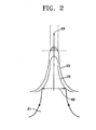
- FIG. 2 The principle enabling patterns finer than the diffraction limit of activation light used to be formed is illustrated in FIG. 2 .
- FIG. 2 is a graph of light intensity and temperature distributions when activation light is incident on a light-to-heat converting layer.
- activation light 21 incident on the light-to-heat converting layer with a spot diameter 20 has a Gaussian intensity distribution 22 where the intensity is peak at the spot center.
- the temperature of the light-to-heat converting layer has a Gaussian distribution.
- a region 24 is an effective region of the photo and thermal sensitive layer 5 (refer to FIG. 1 ) where chemical reaction is induced due to a high temperature and is narrower than the spot diameter 20.
- the Gaussian temperature distribution of the light-to-heat converting layer 22 that renders a reaction region narrower than the spot diameter 21 is important.
- the intensity of activation light or activation light irradiation duration may be further varied to control the heat generation in the first and second light-to-heat converting layers 3 and 7.
- thermal chemical reaction is induced only in a small region of the photo and thermal sensitive material layer that is irradiated by the spot center of the activation light, thereby enabling patterns finer than the diffraction limit of the activation light to be formed.
- the temperature of the first and second light-to-heat converting layers 3 and 4 may rise above hundreds of Celsius. To prevent problems arising from such a temperature rise, the substrate protective layer 2 is formed on the substrate 1.
- the substrate protective layer 2 is formed on the surface of the target substrate 1.
- Suitable materials for the substrate protective layer 2 include inorganic compounds, such as ZnS ⁇ SiO 2 , and organic compounds, such as polyimide.
- the thickness of the substrate protective layer 2 may be, but is not limited to, in a range of 50-500 nm, depending on the wavelength of activation light used and the material properties of the substrate protective layer 2. When the target substrate 1 is thermally resistant, the substrate protective layer 2 is unnecessary.
- the photo and thermal sensitive material layer 5 may be abruptly deformed, evaporate, or swell.
- the first and second thermal buffer layers 4 and 6 are formed between the photo and thermal sensitive material layer 5 and the respective first and second light-to-heat converting layers 3 and 7.
- Materials for the first and second thermal buffer layers 4 and 6 may be the same as materials for the substrate protective layer 2.
- the thicknesses of the first and second thermal buffer layers 4 and 6 are in a range of 5-100 nm, and preferably, 10-50 nm. The thickness of the first and second thermal buffer layers 4 and 6 influences heat diffusibility and pattern shape.
- the thickness of the first and second thermal buffer layers 4 and 6 is smaller than a desired pattern size.
- the first and second thermal buffer layers 4 and 6 may be not formed. Alternatively, any one of the first and second thermal buffer layers 4 and 6 may be formed if required.
- the cap layer 10 may be formed on the second light-to-heat converting layer 7.
- Suitable materials for the cap layer 10 include transparent plastics, transparent glass, dielectric materials, etc.
- the thickness of the cap layer 10 may be, but is not limited to, in a range of 5-200 nm, and preferably, 10-50 nm.
- the cap layer 10 may be not formed when the photo and thermal sensitive material layer 5 is thermally resistant or when certain activation light irradiation conditions prevail.
- the target substrate 1 which are compatible with pattern forming materials according to the present invention having the above-described structure include common materials for substrates used to manufacture electronic/electrical parts by general lithography.
- the target substrate 1 may be an inorganic substrate made of, for example, silicon, tantalum, aluminum, or gallium-arsenic; a glass substrate; or a plastic substrate made of, for example, polypropylene, acrylic resins, polycarbonate, polystyrene resins, or vinylchloride resins.
- an inorganic substrate made of aluminum, tantalum, silica, etc. or a glass substrate with an aluminum or tantalum layer deposited thereon or with a light curing resin layer coated thereon may be used.
- any material which changes in properties by heat or activation light irradiation and which allows a sharp pattern to appear through development processes can be used for the photo and thermal sensitive material layer 5.
- Examples of such a material include positive type and negative type photoresists which have been commonly used so far to manufacture electronic/electrical parts by lithography.
- electron beam resist that thermally changes can be used.
- any material capable of absorbing light and converting it into heat can be used for the first and second light-to-heat converting layers 3 and 7.
- Examples of such a material include: Ge-Sb-Te alloys, including Ge 2 Sb 2 Te 5 used for a recording layer of DVD-RAMs; Sb; Ag-In-Sb-Te alloys; Ag-In-Sb-Te-V alloys; lithium niobate; methylnitro aniline, etc.
- the thickness of the photo and thermal sensitive material layer 5 is in a range of 10-1000 nm, and preferably, 50-200 nm.
- the thicknesses of the first and second light-to-heat converting layers 3 and 7 are in a range of 5-300 nm, and preferably, 10-150 nm.
- the thickness of the first and second light-to-heat converting layers 3 and 7 is not limited to the above range and is varied depending on the wavelength of activation light used and the material composing the first and second light-to-heat converting layers 3 and 7.
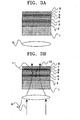
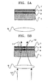
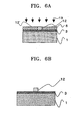
- FIGS. 3A, 3B , 4C, and 4D are sectional views illustrating a method of forming a fine pattern according to an embodiment of the present invention.
- elements that appeared in previous drawings are designated by the same reference numerals.
- pattern forming materials including the first light-to-heat converting layer 3, the first thermal buffer layer 4, the photo and thermal sensitive material layer 5, the second thermal buffer layer 6, the second light-to-heat converting layer 7, and the cap layer 8 are formed on the target substrate 1, with the substrate protective layer 2 between the first light-to-heat converting layer 3 and the target substrate 1.
- the photo and thermal sensitive material layer 5 is made of a positive type photoresist.
- the lens 9 which converges activation light is installed below the target substrate 1.
- the activation light 10 for example, a laser beam
- the activation light is radiated to generate heat in the first and second light-to-heat converting layers 3 and 7 and selectively heat a portion of the photo and thermal sensitive material layer 5 made of a positive type photoresist to form the pattern portion 12, which is no longer photosensitive due to the exposure to heat. Since the photo and thermal sensitive material layer 5 is interposed between the first and second light-to-heat converting layers 3 and 7, both surfaces of the photo and thermal sensitive layer 5 are efficiently heated, thereby enabling a fine high aspect ratio pattern to be formed.
- activation light 13 for example, blue light
- activation light 13 is radiated over the entire exposed surface of the photo and thermal sensitive layer 5.
- a non-pattern portion 12' around the pattern portion 12 is changed to be soluble in a developing solution through a reaction with the blue light 13.
- the blue light 13 is radiated before the second thermal buffer layer 6, the second light-to-heat converting layer 7, and the cap layer 8 are removed.
- the second thermal buffer layer 6, the second light-to-heat converting layer 7, and the cap layer 8 deposited on the photo and thermal sensitive material layer 5 can be removed by dry etching or wet etching.
- Suitable dry etching methods include reactive ion etching (RIE), sputtering etching, etc. HF, KOH, HCl, and other kinds of etchant can be used for wet etching.
- RIE reactive ion etching
- HF, KOH, HCl, and other kinds of etchant can be used for wet etching.
- the method and etchants which can be used to remove the above layers are not limited to the above.
- activation light 10 used in the process of FIG. 3B and the activation light 13 used in the process of FIG. 4C may have different wavelengths or the same wavelength.
- a suitable activation light source is chosen depending on the properties of the photo and thermal sensitive material used. Suitable activation light sources include visible light, deep UV, I-ray, g-ray, KrF eximer laser, ArF eximer layer, etc.
- FIGS. 5A, 5B , 6C, and 6D are sectional views illustrating a method of forming a fine pattern according to another embodiment of the present invention.
- elements that appeared in previous drawings are designated by the same reference numerals.
- pattern forming materials including the first light-to-heat converting layer 3, the photo and thermal sensitive material layer 5, and the second light-to-heat converting layer 7 are formed on the target substrate 1.
- the substrate protective layer 2, the first thermal buffer layer 4, the second thermal buffer layer 6, and the cap layer 8, which are formed in the previous embodiment, may be not formed.
- Such thermal protective layers and cap layer may be not formed depending on the thermal resistance of the target substrate 1 and the photo and thermal sensitive material layer 5 and activation light irradiation conditions, for example, the intensity of activation light.
- the activation light 10 for example, a laser beam
- the activation light is radiated to generate heat in the first and second light-to-heat converting layers 3 and 7 and selectively heat a portion of the photo and thermal sensitive material layer 5 made of a positive type photoresist to form the pattern portion 12, which is no longer photosensitive due to the exposure to heat. Since the photo and thermal sensitive material layer 5 is interposed between the first and second light-to-heat converting layers 3 and 7, both surfaces of the photo and thermal sensitive layer 5 are efficiently heated, thereby enabling a fine high aspect ratio pattern to be formed.
- activation light 13 for example, blue light
- activation light 13 is radiated over the entire exposed surface of the photo and thermal sensitive layer 5.
- a non-pattern portion 12' around the pattern portion 12 is changed to be soluble in a developing solution through a reaction with the blue light 13.
- the blue light 13 is radiated before the second light-to-heat converting layer 7 is removed.
- FIGS. 7A, 7B , 8C, and 8D are sectional views illustrating a method of forming a fine pattern according to another embodiment of the present invention.
- elements that appeared in previous drawings are designated by the same reference numerals.
- FIGS. 7A , 8C, and 8D are the same as the processes illustrated in FIGS. 3A , 4C, and 4D of the second embodiment described above, and thus descriptions thereon will be not repeated here.
- lamp heaters 13 which emit activation light 15 having a long wavelength to heat the target substrate 1 are disposed near the lens 9. Since the photo and thermal sensitive material layer 5 is also heated by the additional lamp heaters 13, a larger amount of heat is generated in the first and second light-to-heat converting layers 3 and 7, and a thermal reaction in the photo and thermal sensitive material layer 5 is facilitated. Accordingly, a smaller amount of activation light 10 can be radiated.
- any heating device can be used for the lamp heaters 13.
- an electrical heater such as a resistor heater, may be installed on a support (not shown) of the target substrate 1.
- FIGS. 9A, 9B , 10C , and 10D are sectional views illustrating a method of forming a fine pattern according to another embodiment of the present invention.
- elements that appeared in previous drawings are designated by the same reference numerals.
- FIG. 9A The structure of pattern forming materials shown in FIG. 9A is the same as the structure illustrated in FIG. 3A .
- the activation light 13 is radiated onto the structure of the pattern forming materials to make the entire photo and thermal sensitive material layer 5 soluble in a developing solution.
- the activation light 13 may be radiated before the second thermal buffer layer, the second light-to-heat converting layer 7, and the cap layer 8 are formed.
- the activation light 10 for example, a laser beam
- the activation light 10 is radiated to generate heat 11 in the first and second light-to-heat converting layers 3 and 7 and selectively heat a portion of the photo and thermal sensitive material layer 5 made of a positive type photoresist to form the pattern portion 12, which is rendered insoluble in a developing solution.
- protons (H + ) are generated in the photo and thermal sensitive material layer 5 and catalyze a cross-linking reaction of the positive type resist composing the photo and thermal sensitive material layer 5 when heated.
- the positive type photoresist is changed to be insoluble in a developing solution. Since the photo and thermal sensitive material layer 5 is interposed between the first and second light-to-heat converting layers 3 and 7, both surfaces of the photo and thermal sensitive layer 5 are efficiently heated, thereby enabling a fine high aspect ratio pattern to be formed.
- the second thermal buffer layer 6, the second light-to-heat converting layer 7, and the cap layer 8 are removed.
- a developing process is performed to remove the non-pattern portion 12' so that only the pattern portion 12 made of resist remains as a fine pattern.
- FIGS. 11A, 11B , 12C, and 12D An embodiment using a negative type photoresist will be described with reference to FIGS. 11A, 11B , 12C, and 12D.
- FIGS. 11A, 11B , 12C, and 12D elements that appeared in previous drawings are designated by the same reference numerals.
- a structure of pattern forming materials which is the same as the structure of the pattern forming materials illustrated in FIG. 3A , except that a negative type photoresist is used for the photo and thermal sensitive material layer 5, is formed.
- the activation light 10 for example, a laser beam
- the activation light is radiated to generate heat 11 in the first and second light-to-heat converting layers 3 and 7 and selectively heat a portion of the photo and thermal sensitive material layer 5 made of a negative type photoresist to form the pattern portion 12.
- the pattern portion 12 is changed to be insoluble in a developing solution.
- FIGS. 12C and 12D are the same as the processes illustrated in FIGS. 10D and 10E in the fifth embodiment.
- the second thermal buffer layer 6, the second light-to-heat converting layer 7, and the cap layer 8 are removed, and the non-pattern portion 12' is removed through a developing process so that only the pattern portion 12 remains as a fine pattern.
- a high aspect ratio fine pattern can be formed with a negative photoresist as well as a positive photoresist.
- a structure of pattern forming materials as illustrated in FIG. 3A in the second embodiment was manufactured with a carbonate substrate having a thickness of 600 nm for the target substrate 1, a ZnS ⁇ SiO 2 layer having a thickness of 200 nm for the substrate protective layer 2, a Ge 2 Sb 2 Te 5 layer having a thickness of 15 nm for each of the first and second light-to-heat converting layers 3 and 7, a ZnS ⁇ SiO 2 layer having a thickness of 20 nm for each of the first and second thermal buffer layers 4 and 6, a ZnS ⁇ SiO 2 layer having a thickness of 20 nm for the cap layer 8, and a positive type photoresist layer (AZ5214-e, available from Clariant Corporation) having a thickness of 70 nm for the photo and thermal sensitive material layer 5.
- AZ5214-e available from Clariant Corporation
- the target substrate 1 with the pattern forming materials was loaded on a disc, and a laser beam having a wavelength of 635 nm was radiated onto the target substrate 1.
- An optical system having a numerical aperture of 0.6 and a diffraction limit of 530 nm was used. Due to the diffraction limit, a pattern finer than the diffraction limit cannot be formed when the optical system is used alone without heating.
- the structure of the pattern forming materials was rotated at a rate of 6 m/s using an optical disc drive tester and irradiated with laser light at 3 mW during a single turn. Next, a line pattern was drawn by laser irradiation of 300 nm from a position closer to the structure of the pattern forming materials.
- a 1% hydrofluoric acid solution was used to remove the cap layer 8 and the second thermal buffer layer 6, and a 1:5 mixture of 10% potassium hydroxide solution and 35% hydrogen peroxide solution was used to remove the second light-to-heat converting layer 7.
- An organic alkaline solution (NMD-W, available from Tokyo Ohka Kogyo Ltd.) was used as a developing solution,
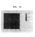
- the resulting fine pattern was observed using an atomic force microscope.
- the result is shown in FIG. 13 .
- the arrows denote the line pattern.
- lines are arranged close together with a line width of 130 nm.
- the maximum height of a single line is 60nm, which is almost the same as the thickness of the photoresist layer.
- the line pattern has a whole shape because there was no evaporation and deformation of the photoresist and has a higher aspect ratio than conventional patterns.
- optical system used in this embodiment which emits visible laser light, is more economical than currently available photolithography which uses vacuum UV, X-rays, etc. , to form a fine pattern.
- a photo and thermal sensitive material layer with light-to-heat converting layers on its upper and lower surfaces is deposited on a target substrate and subjected to activation light irradiation, so that a fine pattern can be efficiently formed in the photo and thermal sensitive material layer by heat generated via the activation light irradiation, without evaporation or deformation of the photo and thermal sensitive material layer.
- the resulting fine pattern has a higher aspect ratio compared to when using conventional methods.
Abstract
Description
- The present invention relates to micromachining of a substrate, and more particularly, to a material for use in forming a fine pattern on a substrate and a method of forming a fine pattern using the material.
- Intensive research on fine patterning methods, such as photolithography, using vacuum ultraviolet rays (VUV) or X-rays, which are applied in the manufacture of semiconductor integrated circuits or electronic/electrical parts, including optical discs, has been conducted. Fine pattern structures with a line width of 0.1 m can be realized in current situations based on such patterning techniques, and their commercialization is expected in a few years.
- A conventional method of forming a resist pattern in the manufacture of electronic/electrical parts involves activation light irradiation onto a photoresist layer through a predetermined mask pattern and development. Accordingly, the minimal dimensions of the resist pattern is limited, in practice, to be slightly smaller than the wavelength of activation light used, due to diffraction of the activation light. The diffraction limit relies on the wavelength of light and the numerical aperture of a lens used. Shorter wavelength of light and greater numerical aperture of a lens are more effective to reduce the diffraction limit. However, since increasing the numerical aperture of the lens has encountered limitations in the current technical status, there are more trends toward using shorter wavelength light to form smaller resist patterns.
- New exposure technology using deep UV, laser light, or soft X-ray has been researched. In current situations, it is possible to form a fine pattern of about 150 nm in size using KrF eximer laser or ArF eximer laser. However, there are needs for improvements in accompanying techniques, for example, regarding the development of high-performance light sources, or property improvements of optical materials or resist materials. Furthermore, there are also needs for technology that allows for the use of smaller light sources or optical systems and saves energy.
- Electron beam lithography ensures much finer pattern processing for a few nanometer pattern dimension compared to photolithography. However, electron beam lithography requires an additional vacuum enclosure, a large electrode, and a high power source for electron acceleration or deflection. Also, the use of a high accelerating voltage of tens of kilovolts raises safety concerns.
- In addition, using smaller wavelength of light or electron beam to form fine patterns in the above-described techniques is cost high. To overcome such defects in the conventional fine pattern formation methods, various methods of forming fine patterns have been suggested. For example, Japanese Patent Application No.
hei 8-249493 - A pattern forming material which thermally changes by activation light irradiation and a patterning method using the material are suggested (Microelectronic Engineering 61-62, 2002, p. 415-421). In this disclosure, a light-to-heat converting material layer made of Ge2Sb2Te5 is interposed between a target substrate and a photoresist layer to be patterned and is subjected to activation light irradiation to generate heat. The heat generated in the Ge2Sb2Te5 layer is transferred to the overlying photoresist layer to induce chemical reactions and form a fine pattern therein. A pattern of 100 nm can be formed with this method. In addition, since a low cost semiconductor laser is used as an activation light source and energy consumption is small, compared to techniques which require costly high-performance light sources, such as KrF eximer laser, ArF eximer laser, or electron beams, the disclosed method is regarded to be very economical and offers higher processing precision and finer pattern processing ability compared to the method using chalcogenide.
- However, the above resist patterning method using the light-to-heat converting material layer has the following limitations. The amount of heat transferred from the light-to-heat converting layer to the photoresist layer is not enough to form a desired fine pattern. The maximum pattern height that can be obtained with this method is limited to 30 nm when the width of a pattern is designed at 100 nm. In other words, this method cannot be applied to form a high aspect ratio pattern on a substrate. When the intensity of laser light radiated is increased to generate larger amount of heat or for higher processing rate or greater pattern height, the photoresist layer undesirably evaporates and disappears.
- The present invention provides new pattern forming materials useful for a high aspect ratio fine pattern and a pattern formation method using the materials.
- The present invention provides a method of efficiently forming a high aspect ratio fine pattern in a thermal sensitive material layer formed on a target substrate using heat generated at first and second light-to-heat converting layer formed on both surfaces of the thermal sensitive material layer, via activation light irradiation.
- In accordance with an aspect of the present invention, there are provided pattern forming materials comprising: a thermal sensitive material layer formed over a target substrate; a first light-to-heat converting layer formed between the thermal sensitive material layer and the target substrate; and a second light-to-heat converting layer formed on a surface of the thermal sensitive material layer opposite to the first light-to-heat converting layer, the thermal sensitive material layer being interposed between the first and second light-to-heat converting layers.
- In accordance with another aspect of the present invention, there is provided a method of forming fine patterns using the above pattern forming materials.
- According to the present invention, since the photo and thermal sensitive material layer is interposed between the first and second light-to-heat converting layers, both surfaces of the photo and thermal sensitive material layer are efficiently heated by activation light irradiation without evaporation or deformation thereof. A resulting fine pattern has a whole shape and a higher aspect ratio.
-
-
FIG. 1 is a sectional view illustrating an exemplary structure of pattern forming materials and the principle of patterning using the pattern forming materials according to the present invention; -
FIG. 2 is a graph of light intensity and temperature distributions when activation light is incident on a light-to-heat converting layer; -
FIGS. 3 and4 are sectional views illustrating a method of forming a fine pattern according to a second embodiment of the present invention; -
FIGS. 5 and6 are sectional views illustrating a method of forming a fine pattern according to a third embodiment of the present invention; -
FIGS. 7 and8 are sectional views illustrating a method of forming a fine pattern according to a fourth embodiment of the present invention; -
FIGS. 9 and10 are sectional views illustrating a method of forming a fine pattern according to a fifth embodiment of the present invention; -
FIGS. 11 and12 are sectional views illustrating a method of forming a fine pattern according to a sixth embodiment of the present invention; and -
FIG. 13 illustrates the result of an atomic force microscopic observation on a fine pattern formed in a seventh embodiment of the present invention. - Hereinafter, embodiments of the present invention will be described in detail with reference to the appended drawings.
-
FIG. 1 illustrates an exemplary structure of pattern forming materials according to the present invention and the principle of forming a fine pattern using the pattern forming materials. The pattern forming materials ofFIG. 1 include a first light-to-heat converting layer 3, a firstthermal buffer layer 4, a photo and thermalsensitive material layer 5, a secondthermal buffer layer 6, a second light-to-heat converting layer 7, and acap layer 8, which are sequentially stacked upon one another, with a substrateprotective layer 2 between the first light-to-heat converting layer 3 and atarget substrate 1. Whenactivation light 10 is radiated onto the pattern forming materials having the above structure via alens 9, the energy of theactivation light 10 is converted intoheat 11 by the function of the first and second light-to-heat converting layers heat 11 is transferred via the first and secondthermal buffer layers pattern portion 12 of the photo and thermalsensitive material layer 5 and induce chemical reaction therein. Although theactivation light 10 is illustrated as being radiated through thetarget substrate 1, theactivation light 10 may be radiated in a direction opposite to thetarget substrate 1 if necessary. The thickness of each layer is determined to be in a range of 2-200 nm. However, each layer may be formed to be thinner or thicker than the above range depending on a desired pattern size or the material composing the photo and thermalsensitive material layer 5. - The
activation light 10 is not fully absorbed by the first light-to-heat converting layer 3, and a large portion of theactivation light 10 transmits the first light-to-heat converting layer 3. The transmitted portion of theactivation light 10 is absorbed and converted into heat by the second light-to-heat converting layer 7. Comparing to conventional one having only one light-to-heat converting layer, theactivation light 10 can be more efficiently converted into heat even at a low output power. Therefore, a conventional problem that the photo and thermal sensitive material layer evaporates due to an excess increase in the output power of the activation light does not arise. As such, theactivation light 10 is absorbed and converted into heat by the first and second light-to-heat converting layers activation light 10 conducts to the photo and thermalsensitive material layer 5 to induce chemical reaction in thepattern portion 12. Subsequently, a reaction domain or a non-reaction domain is etched away to form a desired pattern. - The principle enabling patterns finer than the diffraction limit of activation light used to be formed is illustrated in
FIG. 2 . -
FIG. 2 is a graph of light intensity and temperature distributions when activation light is incident on a light-to-heat converting layer. Referring toFIG. 2 ,activation light 21 incident on the light-to-heat converting layer with aspot diameter 20 has aGaussian intensity distribution 22 where the intensity is peak at the spot center. The temperature of the light-to-heat converting layer has a Gaussian distribution. Aregion 24 is an effective region of the photo and thermal sensitive layer 5 (refer toFIG. 1 ) where chemical reaction is induced due to a high temperature and is narrower than thespot diameter 20. The Gaussian temperature distribution of the light-to-heat converting layer 22 that renders a reaction region narrower than thespot diameter 21 is important. Based on such a temperature distribution of the first and second light-to-heat converting layer FIG. 1 , the intensity of activation light or activation light irradiation duration may be further varied to control the heat generation in the first and second light-to-heat converting layers - In a conventional structure including only one light-to-heat converting layer beneath a photo and thermal sensitive material layer, a limited amount of heat is transferred to the photo and thermal sensitive material layer so that thermal reaction therein is not sufficient to form a high aspect ratio fine pattern. However, according to the present invention, since the photo and thermal
sensitive material layer 5 is inserted between the first and second light-to-heat converting layers sensitive material layer 5 are heated with higher efficiency, thereby enabling a high aspect ratio fine pattern to be formed. - The temperature of the first and second light-to-
heat converting layers protective layer 2 is formed on thesubstrate 1. - In particular, to prevent damage of the
target substrate 1 by the heat generated in the first light-to-heat converting layer 3, the substrateprotective layer 2 is formed on the surface of thetarget substrate 1. Suitable materials for the substrateprotective layer 2 include inorganic compounds, such as ZnS· SiO2, and organic compounds, such as polyimide. The thickness of the substrateprotective layer 2 may be, but is not limited to, in a range of 50-500 nm, depending on the wavelength of activation light used and the material properties of the substrateprotective layer 2. When thetarget substrate 1 is thermally resistant, the substrateprotective layer 2 is unnecessary. - Due to a steep temperature rise by the heat generated in the first and second light-to-
heat converting layers sensitive material layer 5 may be abruptly deformed, evaporate, or swell. To prevent this, the first and second thermal buffer layers 4 and 6 are formed between the photo and thermalsensitive material layer 5 and the respective first and second light-to-heat converting layers protective layer 2. The thicknesses of the first and second thermal buffer layers 4 and 6 are in a range of 5-100 nm, and preferably, 10-50 nm. The thickness of the first and second thermal buffer layers 4 and 6 influences heat diffusibility and pattern shape. It is preferable that the thickness of the first and second thermal buffer layers 4 and 6 is smaller than a desired pattern size. When the photo and thermalsensitive material layer 5 is thermally resistant or when certain activation light irradiation conditions prevail, the first and second thermal buffer layers 4 and 6 may be not formed. Alternatively, any one of the first and second thermal buffer layers 4 and 6 may be formed if required. - In order to prevent abrupt deformation, evaporation, or swelling of the second light-to-
heat converting layer 7 as well as the photo and thermalsensitive material layer 5, thecap layer 10 may be formed on the second light-to-heat converting layer 7. Suitable materials for thecap layer 10 include transparent plastics, transparent glass, dielectric materials, etc. The thickness of thecap layer 10 may be, but is not limited to, in a range of 5-200 nm, and preferably, 10-50 nm. Thecap layer 10 may be not formed when the photo and thermalsensitive material layer 5 is thermally resistant or when certain activation light irradiation conditions prevail. - Materials for the
target substrate 1 which are compatible with pattern forming materials according to the present invention having the above-described structure include common materials for substrates used to manufacture electronic/electrical parts by general lithography. Thetarget substrate 1 may be an inorganic substrate made of, for example, silicon, tantalum, aluminum, or gallium-arsenic; a glass substrate; or a plastic substrate made of, for example, polypropylene, acrylic resins, polycarbonate, polystyrene resins, or vinylchloride resins. Alternatively, an inorganic substrate made of aluminum, tantalum, silica, etc. or a glass substrate with an aluminum or tantalum layer deposited thereon or with a light curing resin layer coated thereon may be used. - Any material which changes in properties by heat or activation light irradiation and which allows a sharp pattern to appear through development processes can be used for the photo and thermal
sensitive material layer 5. Examples of such a material include positive type and negative type photoresists which have been commonly used so far to manufacture electronic/electrical parts by lithography. In addition, electron beam resist that thermally changes can be used. - Any material capable of absorbing light and converting it into heat can be used for the first and second light-to-
heat converting layers - In the pattern forming materials according to the present invention, the thickness of the photo and thermal
sensitive material layer 5 is in a range of 10-1000 nm, and preferably, 50-200 nm. The thicknesses of the first and second light-to-heat converting layers heat converting layers heat converting layers - A method of forming a fine pattern using the above pattern forming materials according to the present invention will be described step by step with reference to the appended drawings.
-
FIGS. 3A, 3B , 4C, and 4D are sectional views illustrating a method of forming a fine pattern according to an embodiment of the present invention. InFIGS. 3A, 3B , 4C, and 4D, elements that appeared in previous drawings are designated by the same reference numerals. - Referring to
FIG. 3A , pattern forming materials including the first light-to-heat converting layer 3, the firstthermal buffer layer 4, the photo and thermalsensitive material layer 5, the secondthermal buffer layer 6, the second light-to-heat converting layer 7, and thecap layer 8 are formed on thetarget substrate 1, with the substrateprotective layer 2 between the first light-to-heat converting layer 3 and thetarget substrate 1. The photo and thermalsensitive material layer 5 is made of a positive type photoresist. Thelens 9 which converges activation light is installed below thetarget substrate 1. - Referring to
FIG. 3B , theactivation light 10, for example, a laser beam, is radiated to generate heat in the first and second light-to-heat converting layers sensitive material layer 5 made of a positive type photoresist to form thepattern portion 12, which is no longer photosensitive due to the exposure to heat. Since the photo and thermalsensitive material layer 5 is interposed between the first and second light-to-heat converting layers sensitive layer 5 are efficiently heated, thereby enabling a fine high aspect ratio pattern to be formed. - Referring to FIG. 4C, after the
thermal buffer layer 6, the second light-to-heat converting layer 7, and thecap layer 8 are removed,activation light 13, for example, blue light, is radiated over the entire exposed surface of the photo and thermalsensitive layer 5. As a result, a non-pattern portion 12' around thepattern portion 12 is changed to be soluble in a developing solution through a reaction with theblue light 13. The same result can be obtained when theblue light 13 is radiated before the secondthermal buffer layer 6, the second light-to-heat converting layer 7, and thecap layer 8 are removed. - Next, a development process is performed to remove the non-pattern portion 12' so that only the
pattern portion 12 made of resist remains. - The second
thermal buffer layer 6, the second light-to-heat converting layer 7, and thecap layer 8 deposited on the photo and thermalsensitive material layer 5 can be removed by dry etching or wet etching. Suitable dry etching methods include reactive ion etching (RIE), sputtering etching, etc. HF, KOH, HCl, and other kinds of etchant can be used for wet etching. However, the method and etchants which can be used to remove the above layers are not limited to the above. - Various kinds of activation light which are commonly used for fine lithography can be selectively used as a light source in the present invention. In addition, the
activation light 10 used in the process ofFIG. 3B and theactivation light 13 used in the process of FIG. 4C may have different wavelengths or the same wavelength. A suitable activation light source is chosen depending on the properties of the photo and thermal sensitive material used. Suitable activation light sources include visible light, deep UV, I-ray, g-ray, KrF eximer laser, ArF eximer layer, etc. -
FIGS. 5A, 5B , 6C, and 6D are sectional views illustrating a method of forming a fine pattern according to another embodiment of the present invention. InFIGS. 5A, 5B , 6C, and 6D, elements that appeared in previous drawings are designated by the same reference numerals. - Referring to
FIG. 5A , pattern forming materials including the first light-to-heat converting layer 3, the photo and thermalsensitive material layer 5, and the second light-to-heat converting layer 7 are formed on thetarget substrate 1. In other words, the substrateprotective layer 2, the firstthermal buffer layer 4, the secondthermal buffer layer 6, and thecap layer 8, which are formed in the previous embodiment, may be not formed. Such thermal protective layers and cap layer may be not formed depending on the thermal resistance of thetarget substrate 1 and the photo and thermalsensitive material layer 5 and activation light irradiation conditions, for example, the intensity of activation light. - Referring to
FIG. 5B , theactivation light 10, for example, a laser beam, is radiated to generate heat in the first and second light-to-heat converting layers sensitive material layer 5 made of a positive type photoresist to form thepattern portion 12, which is no longer photosensitive due to the exposure to heat. Since the photo and thermalsensitive material layer 5 is interposed between the first and second light-to-heat converting layers sensitive layer 5 are efficiently heated, thereby enabling a fine high aspect ratio pattern to be formed. - Referring to FIG. 6C, after the second light-to-
heat converting layer 7 is removed,activation light 13, for example, blue light, is radiated over the entire exposed surface of the photo and thermalsensitive layer 5. As a result, a non-pattern portion 12' around thepattern portion 12 is changed to be soluble in a developing solution through a reaction with theblue light 13. The same result can be obtained when theblue light 13 is radiated before the second light-to-heat converting layer 7 is removed. - Next, a development process is performed to remove the non-pattern portion 12' so that only the
pattern portion 12 made of resist remains. -
FIGS. 7A, 7B , 8C, and 8D are sectional views illustrating a method of forming a fine pattern according to another embodiment of the present invention. InFIGS. 7A, 7B , 8C, and 8D, elements that appeared in previous drawings are designated by the same reference numerals. - The processes illustrated in
FIGS. 7A , 8C, and 8D are the same as the processes illustrated inFIGS. 3A , 4C, and 4D of the second embodiment described above, and thus descriptions thereon will be not repeated here. - Referring to
FIG. 9B ,lamp heaters 13 which emitactivation light 15 having a long wavelength to heat thetarget substrate 1 are disposed near thelens 9. Since the photo and thermalsensitive material layer 5 is also heated by theadditional lamp heaters 13, a larger amount of heat is generated in the first and second light-to-heat converting layers sensitive material layer 5 is facilitated. Accordingly, a smaller amount ofactivation light 10 can be radiated. - Any heating device can be used for the
lamp heaters 13. For example, an electrical heater, such as a resistor heater, may be installed on a support (not shown) of thetarget substrate 1. -
FIGS. 9A, 9B ,10C , and 10D are sectional views illustrating a method of forming a fine pattern according to another embodiment of the present invention. InFIGS. 9A, 9B ,10C , and 10D, elements that appeared in previous drawings are designated by the same reference numerals. - The structure of pattern forming materials shown in
FIG. 9A is the same as the structure illustrated inFIG. 3A . - After the structure of the pattern forming materials has been formed, as illustrated in
FIG. 9B , theactivation light 13 is radiated onto the structure of the pattern forming materials to make the entire photo and thermalsensitive material layer 5 soluble in a developing solution. Alternatively, theactivation light 13 may be radiated before the second thermal buffer layer, the second light-to-heat converting layer 7, and thecap layer 8 are formed. - Next, referring to
FIG. 10C , theactivation light 10, for example, a laser beam, is radiated to generateheat 11 in the first and second light-to-heat converting layers sensitive material layer 5 made of a positive type photoresist to form thepattern portion 12, which is rendered insoluble in a developing solution. In particular, when theactivation light 10 is radiated as illustrated inFIG. 9B , protons (H+) are generated in the photo and thermalsensitive material layer 5 and catalyze a cross-linking reaction of the positive type resist composing the photo and thermalsensitive material layer 5 when heated. As a result, the positive type photoresist is changed to be insoluble in a developing solution. Since the photo and thermalsensitive material layer 5 is interposed between the first and second light-to-heat converting layers sensitive layer 5 are efficiently heated, thereby enabling a fine high aspect ratio pattern to be formed. - Next, referring to FIG. 10D, the second
thermal buffer layer 6, the second light-to-heat converting layer 7, and thecap layer 8 are removed. - Next, referring to FIG. 10E, a developing process is performed to remove the non-pattern portion 12' so that only the
pattern portion 12 made of resist remains as a fine pattern. - Although the above-described embodiments according to the present invention are described as using a positive type photoresist, the same patterning can be performed with a negative type photoresist. An embodiment using a negative type photoresist will be described with reference to
FIGS. 11A, 11B , 12C, and 12D. InFIGS. 11A, 11B , 12C, and 12D, elements that appeared in previous drawings are designated by the same reference numerals. - Referring to
FIG. 11A , a structure of pattern forming materials, which is the same as the structure of the pattern forming materials illustrated inFIG. 3A , except that a negative type photoresist is used for the photo and thermalsensitive material layer 5, is formed. - Next, referring to
FIG. 11B . theactivation light 10, for example, a laser beam, is radiated to generateheat 11 in the first and second light-to-heat converting layers sensitive material layer 5 made of a negative type photoresist to form thepattern portion 12. As a result, thepattern portion 12 is changed to be insoluble in a developing solution. - The processes illustrated in FIGS. 12C and 12D are the same as the processes illustrated in FIGS. 10D and 10E in the fifth embodiment. In other words, the second
thermal buffer layer 6, the second light-to-heat converting layer 7, and thecap layer 8 are removed, and the non-pattern portion 12' is removed through a developing process so that only thepattern portion 12 remains as a fine pattern. - As described above, a high aspect ratio fine pattern can be formed with a negative photoresist as well as a positive photoresist.
- A more specific embodiment of the present invention is described below. The following embodiment is for illustrative purposes and is not intended to limit the scope of the invention.
- A structure of pattern forming materials as illustrated in
FIG. 3A in the second embodiment was manufactured with a carbonate substrate having a thickness of 600 nm for thetarget substrate 1, a ZnS· SiO2 layer having a thickness of 200 nm for the substrateprotective layer 2, a Ge2Sb2Te5 layer having a thickness of 15 nm for each of the first and second light-to-heat converting layers cap layer 8, and a positive type photoresist layer (AZ5214-e, available from Clariant Corporation) having a thickness of 70 nm for the photo and thermalsensitive material layer 5. Next, the structure of the pattern forming materials was patterned using the method described in the above second embodiment. - In particular, the
target substrate 1 with the pattern forming materials was loaded on a disc, and a laser beam having a wavelength of 635 nm was radiated onto thetarget substrate 1. An optical system having a numerical aperture of 0.6 and a diffraction limit of 530 nm was used. Due to the diffraction limit, a pattern finer than the diffraction limit cannot be formed when the optical system is used alone without heating. - The structure of the pattern forming materials was rotated at a rate of 6 m/s using an optical disc drive tester and irradiated with laser light at 3 mW during a single turn. Next, a line pattern was drawn by laser irradiation of 300 nm from a position closer to the structure of the pattern forming materials.
- A 1% hydrofluoric acid solution was used to remove the
cap layer 8 and the secondthermal buffer layer 6, and a 1:5 mixture of 10% potassium hydroxide solution and 35% hydrogen peroxide solution was used to remove the second light-to-heat converting layer 7. An organic alkaline solution (NMD-W, available from Tokyo Ohka Kogyo Ltd.) was used as a developing solution, - The resulting fine pattern was observed using an atomic force microscope. The result is shown in
FIG. 13 . InFIG. 13 , the arrows denote the line pattern. As shown inFIG. 13 , lines are arranged close together with a line width of 130 nm. The maximum height of a single line is 60nm, which is almost the same as the thickness of the photoresist layer. In addition, the line pattern has a whole shape because there was no evaporation and deformation of the photoresist and has a higher aspect ratio than conventional patterns. - The optical system used in this embodiment, which emits visible laser light, is more economical than currently available photolithography which uses vacuum UV, X-rays, etc. , to form a fine pattern.
- While the present invention has been particularly shown and described with reference to exemplary embodiments thereof, it will be understood by those of ordinary skill in the art that various changes in form and details may be made therein without departing from the scope of the present invention as defined by the following claims.
- According to the present invention, a photo and thermal sensitive material layer with light-to-heat converting layers on its upper and lower surfaces is deposited on a target substrate and subjected to activation light irradiation, so that a fine pattern can be efficiently formed in the photo and thermal sensitive material layer by heat generated via the activation light irradiation, without evaporation or deformation of the photo and thermal sensitive material layer. The resulting fine pattern has a higher aspect ratio compared to when using conventional methods.
Claims (19)
- Pattern forming materials comprising:a thermal sensitive material layer formed over a target substrate; anda first light-to-heat converting layer formed between the thermal sensitive material layer and the target substrate; characterised bya second light-to-heat converting layer formed on a surface of the thermal sensitive material layer opposite to the first light-to-heat converting layer,wherein the thermal sensitive material is interposed between the first and second light-to-heat converting layers.
- The pattern forming materials of claim 1, wherein the first and second light-to-heat converting layers absorb activation light radiated thereon and convert the absorbed activation light into heat.
- The pattern forming materials of claim 2, wherein the first and second light-to-heat converting layers comprise a Ge-Sb-Te alloy.
- The pattern forming materials of any one of claims 1 through 3, wherein the thermal sensitive material layer is rendered soluble or insoluble in a developing solution when irradiated further by another activation light.
- The pattern forming materials of claim 4, wherein the thermal sensitive material layer after heat is generated in the first and second light-to-heat converting layers by activation light irradiation is no longer rendered soluble in the developing solution when irradiated further by another activation light.
- The pattern forming materials of claim 4, wherein the thermal sensitive material layer is rendered insoluble in the developing solution by the heat generated in the first and second light-to-heat converting layers by activation light irradiation.
- The pattern forming materials of claim 5, wherein the thermal sensitive material layer is made of a positive type photoresist.
- The pattern forming materials of claim 6, wherein the thermal sensitive material layer is made of a negative type photoresist.
- The pattern forming materials of any one of claim 1 through 8, further comprising at least one thermal protective layer between the second light-to-heat converting layer and the target substrate.
- The pattern forming materials of claim 9, wherein the thermal protective layer is a substrate protective layer formed between the first light-to-heat converting layer and the target substrate.
- The pattern forming materials of claim 9 or 10, wherein the thermal protective layer is a thermal buffer layer formed between the thermal sensitive material layer and the first light-to-heat converting layer.
- The pattern forming materials of any one of claims 9 through 11, wherein the thermal protective layer is a thermal buffer layer formed between the second light-to-heat converting layer and the thermal sensitive material layer.
- The pattern forming materials of any one of claim 1 through 12, further comprising a cap layer on the second light-to-heat converting layer.
- A method of forming a pattern using the pattern forming materials of any one of claims 1 through 13.
- The method of forming a pattern using pattern forming materials of claim 14, the method comprising:(a) radiating activation light onto the first and second light-to-heat converting layers to generate heat therein and change a pattern portion of the thermal sensitive material layer by the heat; and(b) removing a non-pattern portion of the thermal sensitive material layer.
- The method of claim 15, further comprising radiating another activation light onto the thermal sensitive material layer after the pattern portion has been changed.
- The method of claim 15, further comprising radiating another activation light onto the thermal sensitive material layer before step (a).
- The method of any one of claims 15 through 17, wherein the thermal sensitive material layer is made of a positive type photoresist.
- The method of claim 15, wherein the thermal sensitive material layer is made of a negative type photoresist.
Applications Claiming Priority (3)
| Application Number | Priority Date | Filing Date | Title |
|---|---|---|---|
| JP2002308679 | 2002-10-23 | ||
| JP2002308679A JP4221455B2 (en) | 2002-10-23 | 2002-10-23 | Pattern forming material and pattern forming method |
| PCT/KR2003/002192 WO2004038502A1 (en) | 2002-10-23 | 2003-10-20 | Pattern forming materials and pattern formation method using the materials |
Publications (3)
| Publication Number | Publication Date |
|---|---|
| EP1567915A1 EP1567915A1 (en) | 2005-08-31 |
| EP1567915A4 EP1567915A4 (en) | 2009-05-06 |
| EP1567915B1 true EP1567915B1 (en) | 2011-06-08 |
Family
ID=32170982
Family Applications (1)
| Application Number | Title | Priority Date | Filing Date |
|---|---|---|---|
| EP03754229A Expired - Lifetime EP1567915B1 (en) | 2002-10-23 | 2003-10-20 | Pattern forming materials and pattern formation method using the materials |
Country Status (8)
| Country | Link |
|---|---|
| US (1) | US8187786B2 (en) |
| EP (1) | EP1567915B1 (en) |
| JP (1) | JP4221455B2 (en) |
| KR (1) | KR20050073581A (en) |
| CN (1) | CN1705912B (en) |
| AU (1) | AU2003272105A1 (en) |
| TW (1) | TWI228758B (en) |
| WO (1) | WO2004038502A1 (en) |
Families Citing this family (12)
| Publication number | Priority date | Publication date | Assignee | Title |
|---|---|---|---|---|
| KR20060096165A (en) * | 2003-12-09 | 2006-09-07 | 가부시키가이샤 리코 | Structure body and method of producing the structure body, medium for forming structure body, and optical recording medium and method of reproducing the optical recording medium |
| JP4581047B2 (en) * | 2004-08-24 | 2010-11-17 | 独立行政法人産業技術総合研究所 | Pattern forming material, pattern forming method, and optical disc |
| US8859184B2 (en) * | 2005-07-28 | 2014-10-14 | Ricoh Company, Ltd. | Write-once-read-many optical disk having low-to-high recording property accommodating short wavelength recording |
| JP4558641B2 (en) * | 2005-12-27 | 2010-10-06 | 株式会社リコー | Structure forming medium and transferred medium |
| KR100770274B1 (en) | 2007-06-13 | 2007-10-26 | 삼성에스디아이 주식회사 | Method for forming resist pattern |
| TWI417181B (en) * | 2008-01-25 | 2013-12-01 | Asahi Kasei E Materials Corp | The manufacturing method of seamless mold |
| JP4859145B2 (en) * | 2008-12-25 | 2012-01-25 | 独立行政法人産業技術総合研究所 | Etching resist |
| DK2631394T3 (en) | 2009-05-19 | 2015-10-19 | Pacadar Sa | A support structure for a wind turbine |
| JP2012256846A (en) * | 2011-05-16 | 2012-12-27 | Elpida Memory Inc | Manufacturing method of semiconductor device |
| JP6307269B2 (en) * | 2013-04-09 | 2018-04-04 | 旭化成株式会社 | Laminate for forming fine pattern and method for producing mold |
| EP3054351B1 (en) | 2013-09-26 | 2019-01-30 | National Institute for Materials Science | Highly sensitive multilayer resist film and method for improving photosensitivity of resist film |
| CN111367146B (en) * | 2020-04-17 | 2022-08-26 | 苏州科技大学 | Nano photoetching method of phase change-thermal decomposition type composite photoresist |
Family Cites Families (16)
| Publication number | Priority date | Publication date | Assignee | Title |
|---|---|---|---|---|
| JPS6253886A (en) * | 1984-12-26 | 1987-03-09 | Asahi Chem Ind Co Ltd | Information-recording medium |
| JPS6353886A (en) | 1986-08-25 | 1988-03-08 | ソニー株式会社 | Electromagnetic jar |
| US5368986A (en) * | 1991-05-02 | 1994-11-29 | Hitachi, Ltd. | Information recording media, manufacturing method for the same, and information recording method |
| JPH05342629A (en) * | 1992-06-04 | 1993-12-24 | Hitachi Ltd | Information recording medium |
| US5635267A (en) * | 1992-09-17 | 1997-06-03 | Matsushita Electric Industrial Co., Ltd. | Optical information recording medium of phase change type having variably grooved tracks depending on their radial locations |
| WO1996002021A1 (en) * | 1994-07-11 | 1996-01-25 | Konica Corporation | Original form for lithographic plate and process for preparing lithographic plate |
| ES2201474T3 (en) * | 1997-04-16 | 2004-03-16 | Asahi Kasei Kabushiki Kaisha | PROCEDURE FOR THE PRODUCTION OF AN OPTIMAL INFORMATION REGISTRATION MEDIA AND OPTICAL INFORMATION REGISTRATION MEDIA PRODUCED BY THE PROCESS. |
| US6411591B1 (en) * | 1997-09-18 | 2002-06-25 | Hitachi, Ltd. | Optical recording medium and optical memory device |
| JPH11203724A (en) * | 1998-01-09 | 1999-07-30 | Sony Corp | Optical disk and its production |
| JP3500325B2 (en) * | 1998-06-26 | 2004-02-23 | 株式会社東芝 | Phase change recording medium, manufacturing method and manufacturing apparatus thereof |
| JP2000215510A (en) * | 1999-01-22 | 2000-08-04 | Asahi Chem Ind Co Ltd | Optical information recording medium |
| JP2002086945A (en) | 2000-09-12 | 2002-03-26 | Fuji Photo Film Co Ltd | Original plate for thermal lithography |
| US6582890B2 (en) * | 2001-03-05 | 2003-06-24 | Sandia Corporation | Multiple wavelength photolithography for preparing multilayer microstructures |
| ATE360538T1 (en) * | 2001-06-11 | 2007-05-15 | Fujifilm Corp | FLAT PLATE PRECURSOR, SUBSTRATE THEREOF AND HYDROPHILE SURFACE MATERIAL |
| KR100415048B1 (en) * | 2001-06-29 | 2004-01-13 | 한국과학기술연구원 | High density optical recording media |
| EP1418059B1 (en) * | 2001-08-16 | 2006-02-15 | Fuji Photo Film Co., Ltd. | Multicolor image forming material and multicolor image forming method using the same |
-
2002
- 2002-10-23 JP JP2002308679A patent/JP4221455B2/en not_active Expired - Fee Related
-
2003
- 2003-10-01 TW TW092127151A patent/TWI228758B/en not_active IP Right Cessation
- 2003-10-20 CN CN200380101900.5A patent/CN1705912B/en not_active Expired - Fee Related
- 2003-10-20 WO PCT/KR2003/002192 patent/WO2004038502A1/en active Application Filing
- 2003-10-20 EP EP03754229A patent/EP1567915B1/en not_active Expired - Lifetime
- 2003-10-20 KR KR1020057007085A patent/KR20050073581A/en not_active Application Discontinuation
- 2003-10-20 AU AU2003272105A patent/AU2003272105A1/en not_active Abandoned
- 2003-10-20 US US10/531,897 patent/US8187786B2/en not_active Expired - Fee Related
Also Published As
| Publication number | Publication date |
|---|---|
| JP2004144925A (en) | 2004-05-20 |
| TWI228758B (en) | 2005-03-01 |
| KR20050073581A (en) | 2005-07-14 |
| WO2004038502A1 (en) | 2004-05-06 |
| US8187786B2 (en) | 2012-05-29 |
| CN1705912B (en) | 2010-06-16 |
| EP1567915A4 (en) | 2009-05-06 |
| JP4221455B2 (en) | 2009-02-12 |
| AU2003272105A8 (en) | 2004-05-13 |
| AU2003272105A1 (en) | 2004-05-13 |
| EP1567915A1 (en) | 2005-08-31 |
| CN1705912A (en) | 2005-12-07 |
| TW200406824A (en) | 2004-05-01 |
| US20060234168A1 (en) | 2006-10-19 |
Similar Documents
| Publication | Publication Date | Title |
|---|---|---|
| EP1567915B1 (en) | Pattern forming materials and pattern formation method using the materials | |
| JP2013167886A (en) | Dry multilayer inorganic alloy thermal resist for lithographic processing and image formation | |
| US7465530B1 (en) | Inorganic resist material and nano-fabrication method by utilizing the same | |
| KR100630766B1 (en) | Method for forming patterns using phase change material and method for rework thereof | |
| JP2006004594A (en) | Method for forming structure, medium for forming structure, and structure | |
| CN108037636B (en) | Method for manufacturing super-diffraction limit nano-pattern | |
| US4764432A (en) | Photo-mask with regions having a differing optical transmissivities | |
| JP2012088429A (en) | Laminate and method for manufacturing mold using laminate | |
| JP4791653B2 (en) | Fine pattern drawing material, drawing method and fine pattern forming method using the same | |
| US11367617B2 (en) | Graded hardmask interlayer for enhanced extreme ultraviolet performance | |
| JP6307269B2 (en) | Laminate for forming fine pattern and method for producing mold | |
| CN111367146B (en) | Nano photoetching method of phase change-thermal decomposition type composite photoresist | |
| JP4245290B2 (en) | Fine pattern drawing material and fine processing method using the same | |
| JP5545808B2 (en) | Laminated structure | |
| JP2014241183A (en) | Laminate for dry etching, method for manufacturing mold, and mold | |
| US20230019943A1 (en) | Pattern formation method and photosensitive hard mask | |
| JP2630260B2 (en) | Method for forming inorganic resist film | |
| CN101286005B (en) | Local micro photolithography film possessing oxide mask | |
| JP3602594B2 (en) | Method of forming micro optical aperture | |
| EP1370911A4 (en) | Enchanced bright peak clear phase shifting mask and method of use | |
| JP2007172724A (en) | Method for manufacturing stamper | |
| JP2013102079A (en) | Laminate and manufacturing method of mold using the same |
Legal Events
| Date | Code | Title | Description |
|---|---|---|---|
| PUAI | Public reference made under article 153(3) epc to a published international application that has entered the european phase |
Free format text: ORIGINAL CODE: 0009012 |
|
| 17P | Request for examination filed |
Effective date: 20050421 |
|
| AK | Designated contracting states |
Kind code of ref document: A1 Designated state(s): AT BE BG CH CY CZ DE DK EE ES FI FR GB GR HU IE IT LI LU MC NL PT RO SE SI SK TR |
|
| AX | Request for extension of the european patent |
Extension state: AL LT LV MK |
|
| DAX | Request for extension of the european patent (deleted) | ||
| RBV | Designated contracting states (corrected) |
Designated state(s): DE FR GB NL |
|
| RIN1 | Information on inventor provided before grant (corrected) |
Inventor name: TOMINAGA, JUNJI Inventor name: KIM, JOO-HO Inventor name: KUWABARA, MASASHI |
|
| RIN1 | Information on inventor provided before grant (corrected) |
Inventor name: KUWABARA, MASASHI Inventor name: TOMINAGA, JUNJI Inventor name: KIM, JOO-HO |
|
| A4 | Supplementary search report drawn up and despatched |
Effective date: 20090403 |
|
| RIC1 | Information provided on ipc code assigned before grant |
Ipc: B41M 5/26 20060101ALI20090330BHEP Ipc: G03F 1/08 20060101AFI20040511BHEP Ipc: G11B 7/26 20060101ALI20090330BHEP |
|
| 17Q | First examination report despatched |
Effective date: 20090807 |
|
| RAP1 | Party data changed (applicant data changed or rights of an application transferred) |
Owner name: SAMSUNG ELECTRONICS CO., LTD. |
|
| GRAP | Despatch of communication of intention to grant a patent |
Free format text: ORIGINAL CODE: EPIDOSNIGR1 |
|
| GRAS | Grant fee paid |
Free format text: ORIGINAL CODE: EPIDOSNIGR3 |
|
| GRAA | (expected) grant |
Free format text: ORIGINAL CODE: 0009210 |
|
| AK | Designated contracting states |
Kind code of ref document: B1 Designated state(s): DE FR GB NL |
|
| REG | Reference to a national code |
Ref country code: GB Ref legal event code: FG4D |
|
| REG | Reference to a national code |
Ref country code: DE Ref legal event code: R096 Ref document number: 60337360 Country of ref document: DE Effective date: 20110721 |
|
| REG | Reference to a national code |
Ref country code: NL Ref legal event code: VDEP Effective date: 20110608 |
|
| PG25 | Lapsed in a contracting state [announced via postgrant information from national office to epo] |
Ref country code: NL Free format text: LAPSE BECAUSE OF FAILURE TO SUBMIT A TRANSLATION OF THE DESCRIPTION OR TO PAY THE FEE WITHIN THE PRESCRIBED TIME-LIMIT Effective date: 20110608 |
|
| PLBE | No opposition filed within time limit |
Free format text: ORIGINAL CODE: 0009261 |
|
| STAA | Information on the status of an ep patent application or granted ep patent |
Free format text: STATUS: NO OPPOSITION FILED WITHIN TIME LIMIT |
|
| 26N | No opposition filed |
Effective date: 20120309 |
|
| REG | Reference to a national code |
Ref country code: DE Ref legal event code: R097 Ref document number: 60337360 Country of ref document: DE Effective date: 20120309 |
|
| REG | Reference to a national code |
Ref country code: FR Ref legal event code: ST Effective date: 20120629 |
|
| PG25 | Lapsed in a contracting state [announced via postgrant information from national office to epo] |
Ref country code: DE Free format text: LAPSE BECAUSE OF NON-PAYMENT OF DUE FEES Effective date: 20120501 |
|
| REG | Reference to a national code |
Ref country code: DE Ref legal event code: R119 Ref document number: 60337360 Country of ref document: DE Effective date: 20120501 |
|
| PG25 | Lapsed in a contracting state [announced via postgrant information from national office to epo] |
Ref country code: FR Free format text: LAPSE BECAUSE OF NON-PAYMENT OF DUE FEES Effective date: 20111102 |
|
| PGFP | Annual fee paid to national office [announced via postgrant information from national office to epo] |
Ref country code: GB Payment date: 20160921 Year of fee payment: 14 |
|
| GBPC | Gb: european patent ceased through non-payment of renewal fee |
Effective date: 20171020 |
|
| PG25 | Lapsed in a contracting state [announced via postgrant information from national office to epo] |
Ref country code: GB Free format text: LAPSE BECAUSE OF NON-PAYMENT OF DUE FEES Effective date: 20171020 |