EP1566619A2 - Device for remotely stimulating and measuring electronic signals through a fiber optic cable - Google Patents
Device for remotely stimulating and measuring electronic signals through a fiber optic cable Download PDFInfo
- Publication number
- EP1566619A2 EP1566619A2 EP04025049A EP04025049A EP1566619A2 EP 1566619 A2 EP1566619 A2 EP 1566619A2 EP 04025049 A EP04025049 A EP 04025049A EP 04025049 A EP04025049 A EP 04025049A EP 1566619 A2 EP1566619 A2 EP 1566619A2
- Authority
- EP
- European Patent Office
- Prior art keywords
- light beam
- optical
- signal
- electrical
- ream
- Prior art date
- Legal status (The legal status is an assumption and is not a legal conclusion. Google has not performed a legal analysis and makes no representation as to the accuracy of the status listed.)
- Withdrawn
Links
- 239000000835 fiber Substances 0.000 title description 5
- 230000004936 stimulating effect Effects 0.000 title description 4
- 230000003287 optical effect Effects 0.000 claims abstract description 51
- 230000005693 optoelectronics Effects 0.000 claims abstract description 4
- 239000013307 optical fiber Substances 0.000 claims description 15
- 230000004044 response Effects 0.000 claims description 12
- 238000005259 measurement Methods 0.000 claims description 11
- 238000000034 method Methods 0.000 claims description 11
- 238000012360 testing method Methods 0.000 description 11
- 230000005540 biological transmission Effects 0.000 description 6
- 230000007246 mechanism Effects 0.000 description 5
- 238000001514 detection method Methods 0.000 description 4
- 238000004891 communication Methods 0.000 description 3
- 230000000694 effects Effects 0.000 description 3
- 239000004065 semiconductor Substances 0.000 description 3
- 230000008878 coupling Effects 0.000 description 2
- 238000010168 coupling process Methods 0.000 description 2
- 238000005859 coupling reaction Methods 0.000 description 2
- 239000013078 crystal Substances 0.000 description 2
- 230000005684 electric field Effects 0.000 description 2
- 239000000463 material Substances 0.000 description 2
- 238000012986 modification Methods 0.000 description 2
- 230000004048 modification Effects 0.000 description 2
- 239000000523 sample Substances 0.000 description 2
- 238000012546 transfer Methods 0.000 description 2
- DJHGAFSJWGLOIV-UHFFFAOYSA-K Arsenate3- Chemical compound [O-][As]([O-])([O-])=O DJHGAFSJWGLOIV-UHFFFAOYSA-K 0.000 description 1
- JBRZTFJDHDCESZ-UHFFFAOYSA-N AsGa Chemical compound [As]#[Ga] JBRZTFJDHDCESZ-UHFFFAOYSA-N 0.000 description 1
- UFHFLCQGNIYNRP-VVKOMZTBSA-N Dideuterium Chemical compound [2H][2H] UFHFLCQGNIYNRP-VVKOMZTBSA-N 0.000 description 1
- 229910001218 Gallium arsenide Inorganic materials 0.000 description 1
- ZLMJMSJWJFRBEC-UHFFFAOYSA-N Potassium Chemical compound [K] ZLMJMSJWJFRBEC-UHFFFAOYSA-N 0.000 description 1
- 241000656145 Thyrsites atun Species 0.000 description 1
- 238000010521 absorption reaction Methods 0.000 description 1
- FTWRSWRBSVXQPI-UHFFFAOYSA-N alumanylidynearsane;gallanylidynearsane Chemical compound [As]#[Al].[As]#[Ga] FTWRSWRBSVXQPI-UHFFFAOYSA-N 0.000 description 1
- 229940000489 arsenate Drugs 0.000 description 1
- JRPBQTZRNDNNOP-UHFFFAOYSA-N barium titanate Chemical compound [Ba+2].[Ba+2].[O-][Ti]([O-])([O-])[O-] JRPBQTZRNDNNOP-UHFFFAOYSA-N 0.000 description 1
- 229910002113 barium titanate Inorganic materials 0.000 description 1
- 230000008901 benefit Effects 0.000 description 1
- 229910052792 caesium Inorganic materials 0.000 description 1
- TVFDJXOCXUVLDH-UHFFFAOYSA-N caesium atom Chemical compound [Cs] TVFDJXOCXUVLDH-UHFFFAOYSA-N 0.000 description 1
- 239000003990 capacitor Substances 0.000 description 1
- 239000006185 dispersion Substances 0.000 description 1
- 238000003012 network analysis Methods 0.000 description 1
- 229910052700 potassium Inorganic materials 0.000 description 1
- 239000011591 potassium Substances 0.000 description 1
- GNSKLFRGEWLPPA-ZSJDYOACSA-M potassium;dideuterio phosphate Chemical compound [K+].[2H]OP([O-])(=O)O[2H] GNSKLFRGEWLPPA-ZSJDYOACSA-M 0.000 description 1
- 230000008569 process Effects 0.000 description 1
- 230000005701 quantum confined stark effect Effects 0.000 description 1
- 239000010453 quartz Substances 0.000 description 1
- 238000002310 reflectometry Methods 0.000 description 1
- VYPSYNLAJGMNEJ-UHFFFAOYSA-N silicon dioxide Inorganic materials O=[Si]=O VYPSYNLAJGMNEJ-UHFFFAOYSA-N 0.000 description 1
- 230000000638 stimulation Effects 0.000 description 1
- 239000000758 substrate Substances 0.000 description 1
Images


Classifications
-
- G—PHYSICS
- G01—MEASURING; TESTING
- G01M—TESTING STATIC OR DYNAMIC BALANCE OF MACHINES OR STRUCTURES; TESTING OF STRUCTURES OR APPARATUS, NOT OTHERWISE PROVIDED FOR
- G01M11/00—Testing of optical apparatus; Testing structures by optical methods not otherwise provided for
- G01M11/30—Testing of optical devices, constituted by fibre optics or optical waveguides
- G01M11/31—Testing of optical devices, constituted by fibre optics or optical waveguides with a light emitter and a light receiver being disposed at the same side of a fibre or waveguide end-face, e.g. reflectometers
- G01M11/3109—Reflectometers detecting the back-scattered light in the time-domain, e.g. OTDR
- G01M11/3154—Details of the opto-mechanical connection, e.g. connector or repeater
Definitions
- the invention relates to remote electronic testing and measurement and more particularly to systems and methods for remotely stimulating and measuring electronic signals through a fiber optic cable.
- high frequency signals are delivered via coaxial cable or other electrical transmission line, with or without the aid of repeater amplifiers.
- Conventional transmission lines are frequency dispersive, meaning that they distort the delivered signal relative to the sourced or sensed signal by attenuating or excessively delaying higher frequency components of the signal relative to the lower frequency components.
- conventional transmission lines can distort a signal by means of reflections caused by impedance discontinuities along the line. A certain degree of distortion can be tolerated in a communication system, whereas in a measurement system signal distortion must be minimized. Further, in cases where a large dc voltage difference exists between the test instrument and the device being tested or in cases where the presence of a conducting element such as a coaxial cable can disturb the measurement, as for example antenna testing, connections such as coaxial cable are impractical.
- an optoelectronic system in accordance with an embodiment of the invention, includes an optical signal modulator, an optical input guide and an optical output guide connected to the optical signal modulator.
- the system further includes a reflective optical element in the optical signal modulator, the element disposed to reflect an input light beam incident through the optical input guide into an output light beam through the optical output guide.
- the system further includes electrical terminals in the optical signal modulator. The electrical terminals are configured such that an electrical signal on the electrical terminals is operable to interact with the input light beam.
- a method of remote delivery of a modulated signal includes modulating an input light beam with an electrical signal using optical signal modulation, and reflecting the modulated light beam into an output light beam direction different from that of the input light beam.
- FIGURE 1 depicts a system for delivering a copy of an electrical response signal from a remote electrical device under test to an electronic measurement instrument by means of a fiber optic cable, in accordance with embodiments of the invention
- FIGURE 2 depicts a system for remote delivery over an optical fiber link of a modulated signal for stimulating a remote electrical device, in accordance with embodiments of the invention
- FIGURE 3 depicts a system for concurrent delivery over an optical fiber link of stimulus and response signals both to and from a remote electrical device, in accordance with embodiments of the invention
- FIGURE 4A depicts a modulator configuration; including an electroabsorption modulator (EAM), which controls the transmission intensity of a light beam in proportion to applied control voltage;
- EAM electroabsorption modulator
- FIGURE 4B depicts a reflection-mode EAM (REAM) in accordance with embodiments of the invention, combining an EAM with a reflecting surface;
- REM reflection-mode EAM
- FIGURE 5 is a graph of a transfer curve of reflected power-vs-voltage of a typical REAM for constant incident power, in accordance with embodiments of the invention.
- FIGURE 6 depicts a quantum well modulator structure, one example of electroabsorption modulator (EAM);
- FIGURE 7A depicts a REAM configuration biased for linear operation, with AC coupled input signal, in accordance with embodiments of the invention
- FIGURE 7B depicts a differential pair REAM configuration, in accordance with embodiments of the invention.
- FIGURES 8A-8E illustrate REAM configurations for a variety of applications.
- single-mode fiber optic cable is typically of low enough dispersion to cause negligible signal distortion.
- photodetectors and reflection-mode electroabsorption modulators (REAMs) can be designed to have low signal distortion over useful ranges of signal level.
- REMs reflection-mode electroabsorption modulators
- FIGURE 1 depicts system 100 for delivering a copy of an electrical response signal from a remote electrical device under test to an electronic measurement instrument by means of a fiber optic cable, in accordance with embodiments of the invention.
- continuous-wave (CW) light beam 11 launched by CW light source 101 passes through optical circulator 102 and through optical guide 104 as CW light beam 12.
- CW light beam 12 is modulated in an optical signal modulator, for example Reflection Mode Electroabsorption modulator (REAM) 105 at the remote sensing point by remote electrical signal 13 generated by remote electrical device 107.
- RAM Reflection Mode Electroabsorption modulator
- Bias voltage 106 is typically applied to REAM 105 to provide linear operation.
- Modulated light beam 14 is then reflected by REAM 105 back through optical guide 104, optical circulator 102, and optical guide 108 as modulated light beam 15, which is then typically amplified by optical amplifier 109 to provide amplified light beam 16 through optical guide 111.
- This amplified modulated light beam 16 is typically detected by photodetector 110, which generates photoelectric signal 17 through electrical cable 112. Photoelectric signal 17, which replicates remote electrical signal 13, is typically processed by electronic measurement instrument 113.
- FIGURE 2 depicts system 200 for remote delivery over an optical fiber link of a modulated signal for stimulating a remote electrical device, in accordance with embodiments of the invention.
- Modulated light signal 21 from modulated light source 201 passes through optical fiber link 103, optical circulator 102, and as modulated light signal 22 through optical fiber link 104, and impinges on Reflection Mode Electroabsorption Modulator (REAM) 205.
- REAM 205 can be the same as REAM 105 depicted in FIGURE 1.
- REAM 205 typically biased by negative voltage 206, converts modulated light signal 22 to electrical signal 23, which stimulates electrical device being tested 207.
- the response of remote electrical device 207 can be monitored by other means, such that circulator 102, optical amplifier 109, photodetector 110, and electronic measurement instrument 113 need not be used.
- circulator 102, optical amplifier 109, photodetector 110, and electronic measurement instrument 113 need not be used.
- These elements are shown to illustrate the fact that the same apparatus can be used either for stimulus testing as in FIGURE 2 or for response testing as in FIGURE 1, with the difference being whether the light source is CW or modulated.
- FIGURE 3 depicts system 300 for concurrent delivery over an optical fiber link of stimulus and response signals both to and from a remote electrical device, in accordance with embodiments of the invention.
- Modulated light signal 21 from modulated light source 201 passes through optical fiber link 103, optical circulator 102, and as modulated light signal 22 through optical fiber link 104, and impinges on Reflection Mode Electroabsorption Modulator (REAM) 305.
- REAM 305 can be the same as REAM 205 depicted in FIGURE 2.
- REAM 305 typically biased by bias voltage 306 for linear operation, converts modulated light signal 22 to electrical signal 33, which stimulates electrical device being tested 307.
- Electrical device 307 response 34 to stimulation 33, thereby modifying the voltage at its terminals, in turn modulates the reflection coefficient of REAM 305.
- the reflection coefficient of REAM 305 interacts with incident light 22, reflecting a modulated light replica 35 of response voltage 34 through optical guide 104, optical circulator 102, and optical guide segment 108 as modulated light replica 36, which is then typically amplified by optical amplifier 109 and transmitted as amplified modulated light replica 16 through optical guide segment 111 to photodetector 110 and processed by electronic measurement instrument 113.
- a typical application of the configuration shown in FIGURE 3 is Time Domain Reflectometry, but other combined stimulus/response applications could also be performed, for example Network Analysis (Frequency-domain testing of electronic networks).
- REAM represents "Reflection-mode Electroabsorption Modulator.”
- a REAM is essentially an electroabsorption modulator configured to operate in reflection mode, for example by impinging light onto a first face of the modulator and terminating the opposite face of the modulator with a mirror. Reflection modulators have been used with free space optical beams to form communication systems.
- the optical signal modulator can be any type of reflection mode modulator, including: electrooptic (EOM); electromechanical (EMM); and electroabsorption (EAM).
- EOMs electro-optic modulators
- EAM electroabsorption modulator
- EOMs electro-optic modulators
- photodetectors to convert the modulated light to an electrical signal
- the electroabsorption modulator (EAM) which has been advantageously reduced to practice, is believed to be unique among modulator types in having the ability to function as both a modulator and a detector of light.
- FIGURE 4A depicts modulator configuration 400 including electroabsorption modulator (EAM) 401, which controls the transmission intensity of a light beam in proportion to applied control voltage 402.
- EAM 401 modulates the transmitted light so that modulated light 42 exiting the right facet is a time-varying fraction of light 41 entering the left facet, with the time varying fraction being controlled by time varying control voltage 402.
- FIGURE 4B depicts reflection-mode EAM (REAM) 410 in accordance with embodiments of the invention, combining EAM 401 with reflecting surface (e.g., a mirror) 403, having entrance beam 41 and modulated exit beam 43 at the left face of the modulator.
- RAM reflection-mode EAM
- REAM geometry in sensing and probing applications is that only a single optical path is required. If, for example, the optical path is an optical fiber, then the complete assembly can be made much simpler and less complex.
- FIGURE 5 is a graph of a transfer curve of reflected power-vs-voltage of a typical REAM for constant incident power, in accordance with embodiments of the invention.
- Reflected power is displayed along vertical axis 502 as a function of control voltage along the horizontal axis 501.
- Bias voltage is a selected value of control voltage.
- Quantum-confined Stark effect A particular electroabsorption mechanism seen only in quantum wells is called the "quantum-confined Stark effect". This mechanism, like other electroabsorption mechanisms in semiconductors, is also very fast. There are no intrinsic speed limitations on the mechanism itself until timescales well below a picosecond. In practice, speed is limited only by the time taken to apply voltage to the quantum wells, which is typically limited by resistor-capacitance limits of the external circuit. Speeds of 40 GHz have been demonstrated.
- FIGURE 6 depicts quantum well modulator structure 600, one example of electroabsorption modulator (EAM).
- Quantum wells 601 are undoped intrinsic semiconductor layers, sandwiched between p-doped top contact 602 and n-doped bottom contact 603 on n-doped substrate 604. This forms a diode structure, which can be reverse biased through contacts 605, 606, to apply a modulated electric field perpendicular to the quantum well layers. The electric field modulates input light beam 61 to produce output modulated light beam 62.
- Structure 600 is made using gallium arsenide and aluminum gallium arsenide, working best at wavelengths of about 850 nm, although other semiconductor materials may be used. Quantum well structure and operation are further described, for example, in D.A.B. Miller, "Optoelectronic applications of quantum wells," Optics and Photonics News 1, No. 2, pp 7-15, February 1990.
- Electrooptic modulators are typically based on the quadratic (Kerr) electrooptic effect, which is exhibited by crystals such as potassium tantalate niobate or barium titanate. Other electrooptic modulators are based on the linear (Pockels) electrooptic effect, which occurs in crystals such as potassium dideuterium phosphate or cesium dideuterium arsenate. Electromechanical modulators are based on the principles of stress birefringence or photoelasticity, and include a class of acoustooptic modulators using material such as crystalline quartz. Electrooptic and electromechanical modulation are summarized in Hecht, "Optics,” Second Edition, Addison-Wesley Publishing Company, pp. 314-321, 1987.
- FIGURE 7A depicts REAM configuration 700 biased for linear operation, with AC coupled input signal, in accordance with embodiments of the invention.
- Basic REAM device 701 is diagrammed as an electronic diode.
- Bias voltage 71 is applied through bias resistor 703, and electrical signal 72 is coupled in/out through AC coupling capacitor 702.
- Reference voltage 73 is supplied to REAM 701.
- Light beams 74, 75 modulate/are modulated by electrical signal 72.
- the REAM is typically biased, as described in connection with FIGURE 5, and the proper bias voltage does not necessarily coincide with the voltage being sensed. In many cases, AC coupling between the REAM and the voltage under test is required.
- FIGURE 7B depicts differential pair REAM configuration 710, in accordance with embodiments of the invention.
- One way to configure a DC-coupled REAM sensor is to arrange basic REAM devices 701 to operate in differential pairs. Negative bias voltage 71 is applied through respective bias resistors 703, 704, positive bias voltage 70 is applied through bias resistor 705, and electrical signals are connected at 72, 73. Signals can be either modulated voltage signals or DC reference voltages. Light beams 74-77 modulate/are modulated by electrical signals 72, 73.
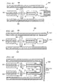
- FIGURES 8A-8E illustrate REAM configurations for a variety of applications.
- FIGURE 8A depicts REAM configuration 800, in which voltage from signal 807 and ground 805 is applied to REAM 801 through contacting probe tips 804, 806 in housing 808, in accordance with embodiments of the invention.
- Input and exit light beams 81, 82 are coupled through lens 802 between optical fiber 803 and REAM 801.
- REAM configuration 800 has high input impedance, such that it presents minimal electrical loading to the signal line.
- FIGURE 8B depicts REAM configuration 820, in which voltage 810, 812 is applied to REAM 801 through non-contacting, electrostatic-coupled probe tips 809, 811 in housing 808, in accordance with embodiments of the invention.
- Input and exit light beams 81, 82 are coupled through lens 802 between optical fiber 803 and REAM 801.
- REAM configuration 820 has high input impedance, such that it presents minimal electrical loading to the signal line.
- FIGURE 8C depicts REAM configuration 840, in which voltage is applied to REAM 801 through impedance matching network 813 attached to coaxial connector 814, in accordance with embodiments of the invention.
- Input and exit light beams 81, 82 are coupled through lens 802 between optical fiber 803 and REAM 801.
- REAM configuration 840 presents a matched load to the coaxial connector (typically 50 ohms).
- FIGURE 8D depicts REAM configuration 860, in which voltage is applied to REAM 801 through terminals of antenna 815, in accordance with embodiments of the invention.
- Antenna 815 may be a single antenna having at least two terminals, one of which can be ground.
- Matching network 813 transforms the REAM impedance to an optimal load for antenna 815.
- Input and exit light beams 81, 82 are coupled through lens 802 between optical fiber 803 and REAM 801.
- FIGURE 8E depicts REAM configuration 880, in which voltage is applied to REAMs 801 through electromagnetic wave directional coupler 816, in accordance with embodiments of the invention.
- the voltage is proportional to the traveling wave amplitude on electromagnetic line 817.
- Input and exit light beams 81, 82 and 83, 84 are coupled through lenses 802 between optical fibers 803 and REAMs 801.
Landscapes
- Physics & Mathematics (AREA)
- Optics & Photonics (AREA)
- Chemical & Material Sciences (AREA)
- Analytical Chemistry (AREA)
- General Physics & Mathematics (AREA)
- Optical Communication System (AREA)
- Optical Modulation, Optical Deflection, Nonlinear Optics, Optical Demodulation, Optical Logic Elements (AREA)
- Arrangements For Transmission Of Measured Signals (AREA)
Abstract
An optoelectronic system 100, 200, 300 includes an optical signal modulator 105,
205, 305, an optical input guide 104 and an optical output 104 guide connected to the optical
signal modulator. The system further includes a reflective optical element 403 in the optical
signal modulator, the element disposed to reflect an input light beam 12 incident through the
optical input guide 104 into an output light beam 14 through the optical output guide 104.
The system further includes electrical terminals 106 in the optical signal modulator. The
electrical terminals are configured such that an electrical signal on the electrical terminals is
operable to interact with the input light beam 12.
Description
The invention relates to remote electronic testing and measurement and
more particularly to systems and methods for remotely stimulating and measuring electronic
signals through a fiber optic cable.
When electrical signals being sourced or sensed are rapidly varying, i.e.
when they contain high frequency components, it is often difficult to deliver these signals to
or from a remote location using conventional means. Typically, high frequency signals are
delivered via coaxial cable or other electrical transmission line, with or without the aid of
repeater amplifiers. Conventional transmission lines are frequency dispersive, meaning that
they distort the delivered signal relative to the sourced or sensed signal by attenuating or
excessively delaying higher frequency components of the signal relative to the lower
frequency components. Also, conventional transmission lines can distort a signal by means
of reflections caused by impedance discontinuities along the line. A certain degree of
distortion can be tolerated in a communication system, whereas in a measurement system
signal distortion must be minimized. Further, in cases where a large dc voltage difference
exists between the test instrument and the device being tested or in cases where the presence
of a conducting element such as a coaxial cable can disturb the measurement, as for example
antenna testing, connections such as coaxial cable are impractical.
In accordance with an embodiment of the invention, an optoelectronic
system is provided. The system includes an optical signal modulator, an optical input guide
and an optical output guide connected to the optical signal modulator. The system further
includes a reflective optical element in the optical signal modulator, the element disposed to
reflect an input light beam incident through the optical input guide into an output light beam
through the optical output guide. The system further includes electrical terminals in the
optical signal modulator. The electrical terminals are configured such that an electrical signal
on the electrical terminals is operable to interact with the input light beam.
In accordance with another embodiment of the invention, a method of
remote delivery of a modulated signal is provided. The method includes modulating an input
light beam with an electrical signal using optical signal modulation, and reflecting the
modulated light beam into an output light beam direction different from that of the input light
beam.
FIGURE 1 depicts a system for delivering a copy of an electrical
response signal from a remote electrical device under test to an electronic measurement
instrument by means of a fiber optic cable, in accordance with embodiments of the invention;
FIGURE 2 depicts a system for remote delivery over an optical fiber
link of a modulated signal for stimulating a remote electrical device, in accordance with
embodiments of the invention;
FIGURE 3 depicts a system for concurrent delivery over an optical fiber
link of stimulus and response signals both to and from a remote electrical device, in
accordance with embodiments of the invention;
FIGURE 4A depicts a modulator configuration; including an
electroabsorption modulator (EAM), which controls the transmission intensity of a light beam
in proportion to applied control voltage;
FIGURE 4B depicts a reflection-mode EAM (REAM) in accordance
with embodiments of the invention, combining an EAM with a reflecting surface;
FIGURE 5 is a graph of a transfer curve of reflected power-vs-voltage of
a typical REAM for constant incident power, in accordance with embodiments of the
invention;
FIGURE 6 depicts a quantum well modulator structure, one example of
electroabsorption modulator (EAM);
FIGURE 7A depicts a REAM configuration biased for linear operation,
with AC coupled input signal, in accordance with embodiments of the invention;
FIGURE 7B depicts a differential pair REAM configuration, in
accordance with embodiments of the invention; and
FIGURES 8A-8E illustrate REAM configurations for a variety of
applications.
It is often necessary or desirable to sense an electrical signal at a
location remote from the measurement instrument that processes the sensed data. Likewise,
it is often necessary to deliver an electronic signal to a location remote from the source of the
signal. Indeed, it is sometimes desirable to both sense and deliver signals remotely with the
same physical apparatus, so that devices being tested can be fully characterized in an efficient
manner.
Over distances conventionally used for remote testing (meters to
hundreds of meters), single-mode fiber optic cable is typically of low enough dispersion to
cause negligible signal distortion. Also, photodetectors and reflection-mode
electroabsorption modulators (REAMs) can be designed to have low signal distortion over
useful ranges of signal level. Thus, the distance between electronic measurement instrument
and location of remote device under test can be increased to distances much greater than
possible with conventional electrical transmission lines, for example coaxial cables.
FIGURE 1 depicts system 100 for delivering a copy of an electrical
response signal from a remote electrical device under test to an electronic measurement
instrument by means of a fiber optic cable, in accordance with embodiments of the invention.
In the remote sensing configuration shown in FIGURE 1, continuous-wave (CW) light beam
11 launched by CW light source 101 passes through optical circulator 102 and through
optical guide 104 as CW light beam 12. CW light beam 12 is modulated in an optical signal
modulator, for example Reflection Mode Electroabsorption modulator (REAM) 105 at the
remote sensing point by remote electrical signal 13 generated by remote electrical device 107.
Bias voltage 106 is typically applied to REAM 105 to provide linear operation. Modulated
light beam 14 is then reflected by REAM 105 back through optical guide 104, optical
circulator 102, and optical guide 108 as modulated light beam 15, which is then typically
amplified by optical amplifier 109 to provide amplified light beam 16 through optical guide
111. This amplified modulated light beam 16 is typically detected by photodetector 110,
which generates photoelectric signal 17 through electrical cable 112. Photoelectric signal 17,
which replicates remote electrical signal 13, is typically processed by electronic measurement
instrument 113.
FIGURE 2 depicts system 200 for remote delivery over an optical fiber
link of a modulated signal for stimulating a remote electrical device, in accordance with
embodiments of the invention. Modulated light signal 21 from modulated light source 201
passes through optical fiber link 103, optical circulator 102, and as modulated light signal 22
through optical fiber link 104, and impinges on Reflection Mode Electroabsorption
Modulator (REAM) 205. REAM 205 can be the same as REAM 105 depicted in FIGURE 1.
REAM 205, typically biased by negative voltage 206, converts modulated light signal 22 to
electrical signal 23, which stimulates electrical device being tested 207. In this case, the
response of remote electrical device 207 can be monitored by other means, such that
circulator 102, optical amplifier 109, photodetector 110, and electronic measurement
instrument 113 need not be used. These elements are shown to illustrate the fact that the
same apparatus can be used either for stimulus testing as in FIGURE 2 or for response testing
as in FIGURE 1, with the difference being whether the light source is CW or modulated.
FIGURE 3 depicts system 300 for concurrent delivery over an optical
fiber link of stimulus and response signals both to and from a remote electrical device, in
accordance with embodiments of the invention. Modulated light signal 21 from modulated
light source 201 passes through optical fiber link 103, optical circulator 102, and as
modulated light signal 22 through optical fiber link 104, and impinges on Reflection Mode
Electroabsorption Modulator (REAM) 305. REAM 305 can be the same as REAM 205
depicted in FIGURE 2. REAM 305, typically biased by bias voltage 306 for linear operation,
converts modulated light signal 22 to electrical signal 33, which stimulates electrical device
being tested 307. Electrical device 307 response 34 to stimulation 33, thereby modifying the
voltage at its terminals, in turn modulates the reflection coefficient of REAM 305. The
reflection coefficient of REAM 305 interacts with incident light 22, reflecting a modulated
light replica 35 of response voltage 34 through optical guide 104, optical circulator 102, and
optical guide segment 108 as modulated light replica 36, which is then typically amplified by
optical amplifier 109 and transmitted as amplified modulated light replica 16 through optical
guide segment 111 to photodetector 110 and processed by electronic measurement instrument
113. A typical application of the configuration shown in FIGURE 3 is Time Domain
Reflectometry, but other combined stimulus/response applications could also be performed,
for example Network Analysis (Frequency-domain testing of electronic networks).
The acronym REAM represents "Reflection-mode Electroabsorption
Modulator." A REAM is essentially an electroabsorption modulator configured to operate in
reflection mode, for example by impinging light onto a first face of the modulator and
terminating the opposite face of the modulator with a mirror. Reflection modulators have
been used with free space optical beams to form communication systems.
The optical signal modulator can be any type of reflection mode
modulator, including: electrooptic (EOM); electromechanical (EMM); and electroabsorption
(EAM). Use of electro-optic modulators (EOMs) to convert electrical signals to modulated
light, and photodetectors to convert the modulated light to an electrical signal is standard
practice in many optical communication systems. The electroabsorption modulator (EAM),
which has been advantageously reduced to practice, is believed to be unique among
modulator types in having the ability to function as both a modulator and a detector of light.
The applications depicted in FIGURES 2 and 3, for example, apply only to the
electroabsorption modulator type.
FIGURE 4A depicts modulator configuration 400 including
electroabsorption modulator (EAM) 401, which controls the transmission intensity of a light
beam in proportion to applied control voltage 402. EAM 401 modulates the transmitted light
so that modulated light 42 exiting the right facet is a time-varying fraction of light 41 entering
the left facet, with the time varying fraction being controlled by time varying control voltage
402. FIGURE 4B depicts reflection-mode EAM (REAM) 410 in accordance with
embodiments of the invention, combining EAM 401 with reflecting surface (e.g., a mirror)
403, having entrance beam 41 and modulated exit beam 43 at the left face of the modulator.
An advantage of the REAM geometry in sensing and probing
applications is that only a single optical path is required. If, for example, the optical path is
an optical fiber, then the complete assembly can be made much simpler and less complex.
FIGURE 5 is a graph of a transfer curve of reflected power-vs-voltage of
a typical REAM for constant incident power, in accordance with embodiments of the
invention. Reflected power is displayed along vertical axis 502 as a function of control
voltage along the horizontal axis 501. Bias voltage is a selected value of control voltage. To
bias the device near the center of the linear operating range, it is necessary to apply a negative
dc bias value, for example voltage 505. This produces an equilibrium reflected power value
504. Linear operation is then achieved centered around bias point 503. Devices can be built
with Vbias=0, but such devices would typically have slow response of reflection to changes
in modulating voltage.
The REAM absorbs light to varying degrees, depending on wavelength
and the particular value of control voltage Vcontrol. Typically, if Vcontrol is zero volts, the
REAM is said to be "transparent", and all light is reflected. If Vcontrol is set to Vbias, then
the REAM operates in a linear region, and the amount of light reflected is linearly
proportional to the applied voltage. Vbias can be used for detection mode, even though
detection efficiency is not maximized. If the REAM is biased, for example, Vbias=-5V, then
nearly all the incoming light is absorbed. This Vbias value can be used for detection mode
operation when maximum detection efficiency and bandwidth are required.
When the REAM is biased to Vcontrol= a negative voltage, light is
absorbed, and the energy of the incoming light is used to create "hole-electron pairs" of
mobile charge. These mobile holes and electrons are swept out of the electrical terminals of
the REAM as a current of flowing charge (photocurrent). This photocurrent has a fast
response time, so that if the incoming light is modulated in intensity, the photocurrent
generated by absorbing this light is modulated also, thereby producing a useful electrical
replica of the modulated light intensity. This operating mechanism, called the photoelectric
effect, which is used traditionally in photodetectors, enables the REAM to be used as a
photodetector.
A basic description of the operation of one example of electro absorption
modulator is available on the internet at:
http://www.bell-labs.com/proiect/oevlsi/tutorial/
http://www.bell-labs.com/proiect/oevlsi/tutorial/
A particular electroabsorption mechanism seen only in quantum wells is
called the "quantum-confined Stark effect". This mechanism, like other electroabsorption
mechanisms in semiconductors, is also very fast. There are no intrinsic speed limitations on
the mechanism itself until timescales well below a picosecond. In practice, speed is limited
only by the time taken to apply voltage to the quantum wells, which is typically limited by
resistor-capacitance limits of the external circuit. Speeds of 40 GHz have been demonstrated.
FIGURE 6 depicts quantum well modulator structure 600, one example
of electroabsorption modulator (EAM). Quantum wells 601 are undoped intrinsic
semiconductor layers, sandwiched between p-doped top contact 602 and n-doped bottom
contact 603 on n-doped substrate 604. This forms a diode structure, which can be reverse
biased through contacts 605, 606, to apply a modulated electric field perpendicular to the
quantum well layers. The electric field modulates input light beam 61 to produce output
modulated light beam 62. Structure 600 is made using gallium arsenide and aluminum
gallium arsenide, working best at wavelengths of about 850 nm, although other
semiconductor materials may be used. Quantum well structure and operation are further
described, for example, in D.A.B. Miller, "Optoelectronic applications of quantum wells,"
Optics and Photonics News 1, No. 2, pp 7-15, February 1990.
Electrooptic modulators are typically based on the quadratic (Kerr)
electrooptic effect, which is exhibited by crystals such as potassium tantalate niobate or
barium titanate. Other electrooptic modulators are based on the linear (Pockels) electrooptic
effect, which occurs in crystals such as potassium dideuterium phosphate or cesium
dideuterium arsenate. Electromechanical modulators are based on the principles of stress
birefringence or photoelasticity, and include a class of acoustooptic modulators using
material such as crystalline quartz. Electrooptic and electromechanical modulation are
summarized in Hecht, "Optics," Second Edition, Addison-Wesley Publishing Company, pp.
314-321, 1987.
FIGURE 7A depicts REAM configuration 700 biased for linear
operation, with AC coupled input signal, in accordance with embodiments of the invention.
Basic REAM device 701 is diagrammed as an electronic diode. Bias voltage 71 is applied
through bias resistor 703, and electrical signal 72 is coupled in/out through AC coupling
capacitor 702. Reference voltage 73 is supplied to REAM 701. Light beams 74, 75
modulate/are modulated by electrical signal 72. As with many electronic devices, the REAM
is typically biased, as described in connection with FIGURE 5, and the proper bias voltage
does not necessarily coincide with the voltage being sensed. In many cases, AC coupling
between the REAM and the voltage under test is required.
FIGURE 7B depicts differential pair REAM configuration 710, in
accordance with embodiments of the invention. One way to configure a DC-coupled REAM
sensor is to arrange basic REAM devices 701 to operate in differential pairs. Negative bias
voltage 71 is applied through respective bias resistors 703, 704, positive bias voltage 70 is
applied through bias resistor 705, and electrical signals are connected at 72, 73. Signals can
be either modulated voltage signals or DC reference voltages. Light beams 74-77
modulate/are modulated by electrical signals 72, 73.
FIGURES 8A-8E illustrate REAM configurations for a variety of
applications. FIGURE 8A depicts REAM configuration 800, in which voltage from signal
807 and ground 805 is applied to REAM 801 through contacting probe tips 804, 806 in
housing 808, in accordance with embodiments of the invention. Input and exit light beams
81, 82 are coupled through lens 802 between optical fiber 803 and REAM 801. REAM
configuration 800 has high input impedance, such that it presents minimal electrical loading
to the signal line.
FIGURE 8B depicts REAM configuration 820, in which voltage 810,
812 is applied to REAM 801 through non-contacting, electrostatic-coupled probe tips 809,
811 in housing 808, in accordance with embodiments of the invention. Input and exit light
beams 81, 82 are coupled through lens 802 between optical fiber 803 and REAM 801.
REAM configuration 820 has high input impedance, such that it presents minimal electrical
loading to the signal line.
FIGURE 8C depicts REAM configuration 840, in which voltage is
applied to REAM 801 through impedance matching network 813 attached to coaxial
connector 814, in accordance with embodiments of the invention. Input and exit light beams
81, 82 are coupled through lens 802 between optical fiber 803 and REAM 801. REAM
configuration 840 presents a matched load to the coaxial connector (typically 50 ohms).
FIGURE 8D depicts REAM configuration 860, in which voltage is
applied to REAM 801 through terminals of antenna 815, in accordance with embodiments of
the invention. Antenna 815, as traditionally configured, may be a single antenna having at
least two terminals, one of which can be ground. Matching network 813 transforms the
REAM impedance to an optimal load for antenna 815. Input and exit light beams 81, 82 are
coupled through lens 802 between optical fiber 803 and REAM 801.
FIGURE 8E depicts REAM configuration 880, in which voltage is
applied to REAMs 801 through electromagnetic wave directional coupler 816, in accordance
with embodiments of the invention. The voltage is proportional to the traveling wave
amplitude on electromagnetic line 817. Input and exit light beams 81, 82 and 83, 84 are
coupled through lenses 802 between optical fibers 803 and REAMs 801.
While the invention has been described in conjunction with specific
embodiments, it is evident to those skilled in the art that many alternatives, modifications,
and variations will be apparent in light of the foregoing description. Accordingly, the
invention is intended to embrace all other such alternatives, modifications, and variations that
fall within the spirit and scope of the appended claims.
Claims (10)
- An optoelectronic system 100, 200, 300 comprising:an optical signal modulator 105, 205, 305;an optical input guide 104 and an optical output guide 104 connected to said optical signal modulator;a reflective optical element 403 in said optical signal modulator, said element disposed to reflect an input light beam 12 incident through said optical input guide 104 into an output light beam 14 through said optical output guide 104; andan electrical terminal 106 in said optical signal modulator 105, said electrical terminal configured such that an electrical signal on said electrical terminal is operable to interact with said input light beam 12.
- The system of claim 1 wherein said optical signal modulator 105 is an electroabsorption modulator (EAM) 410.
- The system of claim 2 wherein said input light beam 22 is operable to interact to modulate said electrical signal 23.
- The system of claim 2 wherein said electrical signal 13 is operable to interact to modulate said output light beam 14.
- A method of remote delivery of a modulated signal, said method comprising:modulating an input light beam 12 with an electrical signal 13 using optical signal modulation; andreflecting said modulated light beam 14 into an output light beam direction different from that of said input light beam 12.
- The method of claim 5 further comprising concurrently modulating said electrical signal 33 by interacting with said input light beam 22 using electroabsorption modulation.
- The method of claim 5 wherein said output light beam 14 and said input light beam 12 propagate in opposite directions through a single optical fiber 104.
- The method of claim 5 wherein said input light beam 22 delivers a replica of an electrical stimulus signal 23.
- The method of claim 5 wherein said output light beam 35 delivers a replica of an electrical response signal 34 from a remote electrical device 307 to an electronic measurement instrument 113.
- The method of claim 9 wherein said input light beam 22 delivers a replica of an electrical stimulus signal 33 to a remote electrical device 307.
Applications Claiming Priority (2)
| Application Number | Priority Date | Filing Date | Title |
|---|---|---|---|
| US10/782,051 US7280267B2 (en) | 2004-02-19 | 2004-02-19 | Device for remotely stimulating and measuring electronic signals through a fiber optic cable |
| US782051 | 2004-02-19 |
Publications (1)
| Publication Number | Publication Date |
|---|---|
| EP1566619A2 true EP1566619A2 (en) | 2005-08-24 |
Family
ID=34711858
Family Applications (1)
| Application Number | Title | Priority Date | Filing Date |
|---|---|---|---|
| EP04025049A Withdrawn EP1566619A2 (en) | 2004-02-19 | 2004-10-21 | Device for remotely stimulating and measuring electronic signals through a fiber optic cable |
Country Status (4)
| Country | Link |
|---|---|
| US (1) | US7280267B2 (en) |
| EP (1) | EP1566619A2 (en) |
| JP (1) | JP2005260925A (en) |
| CN (1) | CN1658249A (en) |
Families Citing this family (10)
| Publication number | Priority date | Publication date | Assignee | Title |
|---|---|---|---|---|
| KR20060025743A (en) * | 2004-09-17 | 2006-03-22 | 삼성전자주식회사 | Optical network for two-way wireless communication |
| WO2007118326A1 (en) * | 2006-04-18 | 2007-10-25 | Pyrophotonics Lasers Inc. | Method and system for tunable pulsed laser source |
| FR2901424B1 (en) * | 2006-05-17 | 2008-08-08 | Femlight Sa | IMPULSIVE LASER DEVICE WITH HIGH POWER OPTICAL FIBER |
| US8594469B2 (en) * | 2008-12-22 | 2013-11-26 | Electronics And Telecommunications Research Institute | Optical amplifier |
| US8606110B2 (en) * | 2012-01-08 | 2013-12-10 | Optiway Ltd. | Optical distributed antenna system |
| US9239348B2 (en) | 2013-03-14 | 2016-01-19 | Kirk S. Giboney | Optical modulator directional measurement system |
| GB201411342D0 (en) * | 2014-06-26 | 2014-08-13 | Rolls Royce Plc | Wireless communication system |
| CN109342807B (en) * | 2018-12-17 | 2021-08-27 | 中北大学 | Voltage sensing device combining elastic light modulation and electro-optic modulation and detection method |
| CN110233669B (en) * | 2019-07-25 | 2024-12-06 | 重庆金山医疗技术研究院有限公司 | Endoscope system using illumination optical communication |
| US11874538B2 (en) | 2020-09-30 | 2024-01-16 | Taiwan Semiconductor Manufacturing Company Limited | Apparatus and method for generating an optical signal |
Family Cites Families (6)
| Publication number | Priority date | Publication date | Assignee | Title |
|---|---|---|---|---|
| US5402234A (en) * | 1992-08-31 | 1995-03-28 | Zygo Corporation | Method and apparatus for the rapid acquisition of data in coherence scanning interferometry |
| US5402259A (en) * | 1993-04-23 | 1995-03-28 | Trw Inc. | Linear electroabsorptive modulator and related method of analog modulation of an optical carrier |
| US5898517A (en) * | 1995-08-24 | 1999-04-27 | Weis; R. Stephen | Optical fiber modulation and demodulation system |
| US5966234A (en) * | 1997-06-24 | 1999-10-12 | Lucent Technologies Inc | Retro-reflecting electroabsorption optical modulators |
| JPH11119177A (en) * | 1997-10-13 | 1999-04-30 | Oki Electric Ind Co Ltd | Optical time multiplex modulation transmitter module |
| WO2005029022A1 (en) * | 2003-09-19 | 2005-03-31 | Queen's University At Kingston | Method and apparatus for directly measuring the phase change of an optical signal |
-
2004
- 2004-02-19 US US10/782,051 patent/US7280267B2/en not_active Expired - Fee Related
- 2004-10-21 EP EP04025049A patent/EP1566619A2/en not_active Withdrawn
- 2004-11-12 CN CN200410089953.6A patent/CN1658249A/en active Pending
-
2005
- 2005-02-08 JP JP2005031755A patent/JP2005260925A/en active Pending
Also Published As
| Publication number | Publication date |
|---|---|
| CN1658249A (en) | 2005-08-24 |
| JP2005260925A (en) | 2005-09-22 |
| US7280267B2 (en) | 2007-10-09 |
| US20050185246A1 (en) | 2005-08-25 |
Similar Documents
| Publication | Publication Date | Title |
|---|---|---|
| JP2791856B2 (en) | Electric field sensor | |
| EP0664460B1 (en) | Electric field sensor | |
| US5389782A (en) | Optically powered amplifier used by an electromagnetic field sensor to amplify an electrical signal from an antenna | |
| US7280267B2 (en) | Device for remotely stimulating and measuring electronic signals through a fiber optic cable | |
| US8179527B2 (en) | Terahertz spectrometer | |
| US6285182B1 (en) | Electro-optic voltage sensor | |
| JP7398672B2 (en) | Optical electric field sensor head | |
| Rabbani et al. | Microwave photonic IFM receiver with adjustable measurement range based on a dual-output Sagnac loop | |
| US7221813B2 (en) | Signal acquisition probing and voltage measurement systems using an electro-optical cavity | |
| US7310455B2 (en) | Variable attenuation signal acquisition probing and voltage measurement systems using an electro-optical cavity | |
| Masterson et al. | Photonic probes for the measurement of electromagnetic fields over broad bandwidths | |
| JPH10115644A (en) | Optical integrated voltage sensor | |
| US6580540B1 (en) | Time compensation architectures for controlling timing of optical signals | |
| JPH09113557A (en) | Electric field sensor operating point adjustment method and electric field sensor | |
| US7187187B2 (en) | Signal acquisition probing system using a micro-cavity laser | |
| JPH0989961A (en) | Electric field detector | |
| JP2562287Y2 (en) | Electric field antenna | |
| TWI915007B (en) | Detection system and detection method thereof | |
| JP3355503B2 (en) | Electric field sensor | |
| Schwerdt et al. | An integrated optical E-field sensor using a reflection scheme | |
| Bassen et al. | An RF field strength measurement system using unintegrated optical linear modulator | |
| JP3355502B2 (en) | Electric field sensor | |
| JPH0522216B2 (en) | ||
| JPH052043A (en) | Electric field sensor | |
| JP3577616B2 (en) | Electric field sensor |
Legal Events
| Date | Code | Title | Description |
|---|---|---|---|
| PUAI | Public reference made under article 153(3) epc to a published international application that has entered the european phase |
Free format text: ORIGINAL CODE: 0009012 |
|
| AK | Designated contracting states |
Kind code of ref document: A2 Designated state(s): AT BE BG CH CY CZ DE DK EE ES FI FR GB GR HU IE IT LI LU MC NL PL PT RO SE SI SK TR |
|
| AX | Request for extension of the european patent |
Extension state: AL HR LT LV MK |
|
| RAP1 | Party data changed (applicant data changed or rights of an application transferred) |
Owner name: AGILENT TECHNOLOGIES, INC. |
|
| STAA | Information on the status of an ep patent application or granted ep patent |
Free format text: STATUS: THE APPLICATION HAS BEEN WITHDRAWN |
|
| 18W | Application withdrawn |
Effective date: 20091128 |
|
| R18W | Application withdrawn (corrected) |
Effective date: 20091128 |