JP2005260925A - Device for remotely stimulating and measuring electric signals through fiber optic cable - Google Patents
Device for remotely stimulating and measuring electric signals through fiber optic cable Download PDFInfo
- Publication number
- JP2005260925A JP2005260925A JP2005031755A JP2005031755A JP2005260925A JP 2005260925 A JP2005260925 A JP 2005260925A JP 2005031755 A JP2005031755 A JP 2005031755A JP 2005031755 A JP2005031755 A JP 2005031755A JP 2005260925 A JP2005260925 A JP 2005260925A
- Authority
- JP
- Japan
- Prior art keywords
- light beam
- signal
- electrical
- optical
- ream
- Prior art date
- Legal status (The legal status is an assumption and is not a legal conclusion. Google has not performed a legal analysis and makes no representation as to the accuracy of the status listed.)
- Pending
Links
- 239000000835 fiber Substances 0.000 title description 7
- 230000004936 stimulating effect Effects 0.000 title description 2
- 230000003287 optical effect Effects 0.000 claims abstract description 59
- 239000013307 optical fiber Substances 0.000 claims description 13
- 230000004044 response Effects 0.000 claims description 13
- 238000000034 method Methods 0.000 claims description 10
- 238000005259 measurement Methods 0.000 claims description 6
- 230000000638 stimulation Effects 0.000 claims description 3
- 230000005693 optoelectronics Effects 0.000 abstract description 2
- 238000012360 testing method Methods 0.000 description 13
- 230000005540 biological transmission Effects 0.000 description 10
- 238000001514 detection method Methods 0.000 description 10
- 230000007246 mechanism Effects 0.000 description 5
- 230000000694 effects Effects 0.000 description 4
- 238000004891 communication Methods 0.000 description 3
- 239000013078 crystal Substances 0.000 description 3
- 239000004065 semiconductor Substances 0.000 description 3
- 238000010521 absorption reaction Methods 0.000 description 2
- 230000008901 benefit Effects 0.000 description 2
- 230000008878 coupling Effects 0.000 description 2
- 238000010168 coupling process Methods 0.000 description 2
- 238000005859 coupling reaction Methods 0.000 description 2
- 230000005684 electric field Effects 0.000 description 2
- 229910052739 hydrogen Inorganic materials 0.000 description 2
- 239000001257 hydrogen Substances 0.000 description 2
- -1 hydrogen potassium phosphate Chemical class 0.000 description 2
- 239000000463 material Substances 0.000 description 2
- 238000012986 modification Methods 0.000 description 2
- 230000004048 modification Effects 0.000 description 2
- 230000010076 replication Effects 0.000 description 2
- 239000000523 sample Substances 0.000 description 2
- 238000012546 transfer Methods 0.000 description 2
- JBRZTFJDHDCESZ-UHFFFAOYSA-N AsGa Chemical compound [As]#[Ga] JBRZTFJDHDCESZ-UHFFFAOYSA-N 0.000 description 1
- 229910001218 Gallium arsenide Inorganic materials 0.000 description 1
- 230000005374 Kerr effect Effects 0.000 description 1
- 230000005697 Pockels effect Effects 0.000 description 1
- 241000656145 Thyrsites atun Species 0.000 description 1
- VEUKJXRCHYAIAW-UHFFFAOYSA-N [Nb].[K] Chemical compound [Nb].[K] VEUKJXRCHYAIAW-UHFFFAOYSA-N 0.000 description 1
- FTWRSWRBSVXQPI-UHFFFAOYSA-N alumanylidynearsane;gallanylidynearsane Chemical compound [As]#[Al].[As]#[Ga] FTWRSWRBSVXQPI-UHFFFAOYSA-N 0.000 description 1
- 230000002238 attenuated effect Effects 0.000 description 1
- JRPBQTZRNDNNOP-UHFFFAOYSA-N barium titanate Chemical compound [Ba+2].[Ba+2].[O-][Ti]([O-])([O-])[O-] JRPBQTZRNDNNOP-UHFFFAOYSA-N 0.000 description 1
- 229910002113 barium titanate Inorganic materials 0.000 description 1
- 239000003990 capacitor Substances 0.000 description 1
- 230000008859 change Effects 0.000 description 1
- 230000003111 delayed effect Effects 0.000 description 1
- 239000006185 dispersion Substances 0.000 description 1
- 238000003012 network analysis Methods 0.000 description 1
- 229910000160 potassium phosphate Inorganic materials 0.000 description 1
- LWIHDJKSTIGBAC-UHFFFAOYSA-K potassium phosphate Substances [K+].[K+].[K+].[O-]P([O-])([O-])=O LWIHDJKSTIGBAC-UHFFFAOYSA-K 0.000 description 1
- 235000011009 potassium phosphates Nutrition 0.000 description 1
- 230000008569 process Effects 0.000 description 1
- 230000005701 quantum confined stark effect Effects 0.000 description 1
- 239000010453 quartz Substances 0.000 description 1
- 238000002310 reflectometry Methods 0.000 description 1
- VYPSYNLAJGMNEJ-UHFFFAOYSA-N silicon dioxide Inorganic materials O=[Si]=O VYPSYNLAJGMNEJ-UHFFFAOYSA-N 0.000 description 1
- 239000000758 substrate Substances 0.000 description 1
Images


Classifications
-
- G—PHYSICS
- G01—MEASURING; TESTING
- G01M—TESTING STATIC OR DYNAMIC BALANCE OF MACHINES OR STRUCTURES; TESTING OF STRUCTURES OR APPARATUS, NOT OTHERWISE PROVIDED FOR
- G01M11/00—Testing of optical apparatus; Testing structures by optical methods not otherwise provided for
- G01M11/30—Testing of optical devices, constituted by fibre optics or optical waveguides
- G01M11/31—Testing of optical devices, constituted by fibre optics or optical waveguides with a light emitter and a light receiver being disposed at the same side of a fibre or waveguide end-face, e.g. reflectometers
- G01M11/3109—Reflectometers detecting the back-scattered light in the time-domain, e.g. OTDR
- G01M11/3154—Details of the opto-mechanical connection, e.g. connector or repeater
Abstract
Description
本発明は遠隔電気試験および計測に関し、詳しくは光ファイバケーブルを介して遠隔から刺激を与え、電気信号を計測するシステムおよび方法に関する。 The present invention relates to remote electrical testing and measurement, and more particularly to a system and method for remotely stimulating and measuring electrical signals via a fiber optic cable.
発信源の電気信号や検出対象の電気信号が急激な変化を有する場合、すなわち高周波成分を含む場合、それらの電気信号を従来の手段を用いて遠隔地とやりとりすることはしばしば困難になる。一般に高周波信号は同軸ケーブルその他の伝送線路を介して伝送され、中継増幅器の助けを借りる場合もあれば、中継増幅器を必要としない場合もある。 When the electrical signal of the transmission source or the electrical signal to be detected has an abrupt change, that is, when it contains a high frequency component, it is often difficult to exchange these electrical signals with a remote place using conventional means. In general, high-frequency signals are transmitted through coaxial cables or other transmission lines, and may or may not require a relay amplifier.
従来の伝送線路は周波数分散特性を有する。すなわち、伝送信号の高周波成分が低周波成分に対して減衰または過度に遅延され、伝送された信号が発信信号や検出信号に対して歪む性質を持つ。また、従来の伝送線路は、線路のインピーダンスの不均一性によって起こる反射によって信号が歪むこともある。通信システムの場合、或る程度の信号歪みを許容することもできるが、計測システムの場合、信号歪みを最小限に抑えなければならない。さらに、試験機器と試験対象デバイスとの間に大きな直流電圧差がある場合や、同軸ケーブル等の導電素子が存在する場合は、アンテナ試験等の測定に影響を与える可能性があるため、同軸ケーブル等による接続は実用的でない。 Conventional transmission lines have frequency dispersion characteristics. That is, the high frequency component of the transmission signal is attenuated or excessively delayed with respect to the low frequency component, and the transmitted signal is distorted with respect to the transmission signal and the detection signal. Further, in the conventional transmission line, the signal may be distorted by reflection caused by the non-uniformity of the impedance of the line. For communication systems, some degree of signal distortion can be tolerated, but for measurement systems, signal distortion must be minimized. Furthermore, if there is a large DC voltage difference between the test equipment and the device under test, or if there is a conductive element such as a coaxial cable, it may affect measurements such as antenna tests. Connection by etc. is not practical.
本発明は一実施形態において光電気システムを提供する。この光電気システムは、光信号変調器、並びに該光信号変調器に接続された入力光導波路および出力光導波路を含む。このシステムは光信号変調器内に光反射要素をさらに含む。光反射要素は、入力光導波路を通って入射してきた入力光ビームを出力光導波路を通じて出力光ビームとして反射するように配置される。このシステムは光信号変調器内に電気端子をさらに含む。電気端子は、該電気端子上の電気信号を入力光ビームと相互作用させるように構成される。 The present invention in one embodiment provides a photoelectric system. The optoelectric system includes an optical signal modulator and an input optical waveguide and an output optical waveguide connected to the optical signal modulator. The system further includes a light reflecting element within the optical signal modulator. The light reflecting element is arranged to reflect an input light beam incident through the input optical waveguide as an output light beam through the output optical waveguide. The system further includes an electrical terminal within the optical signal modulator. The electrical terminal is configured to interact an electrical signal on the electrical terminal with the input light beam.
本発明は他の実施形態において、変調された信号を遠隔伝送する方法を提供する。この方法は、入力光ビームを光信号変調を用いて電気信号で変調するステップと、変調された光ビームを出力光ビームとして入力光ビームとは異なる方向へ反射させるステップとを含む。 In another embodiment, the present invention provides a method for remotely transmitting a modulated signal. The method includes modulating an input light beam with an electrical signal using optical signal modulation and reflecting the modulated light beam as an output light beam in a different direction from the input light beam.
電気信号の検出は、その検出データを処理する計測機器から離れた場所で行なうことが必要とされたり、望ましい場合がある。同様に、電気信号は、その信号源から離れた場所まで伝送しなければならないことがある。実際、信号の検出と伝送を両方とも同じ物理的装置で行ない、効率的な方法で試験対象デバイスの性質を完全に究明できるようにすることが望ましい場合がある。 It may be necessary or desirable to detect the electrical signal at a location away from the measuring device that processes the detected data. Similarly, an electrical signal may have to be transmitted to a location remote from the signal source. In fact, it may be desirable to perform both signal detection and transmission on the same physical device so that the nature of the device under test can be fully investigated in an efficient manner.
遠隔試験に従来から用いられている距離範囲(数メートルから数百メートルの範囲)においてシングルモード光ファイバケーブルはその拡散性が十分に低く、無視できる程度の信号歪みしか生じない。また、光検出器やREAM(反射モード電界吸収変調器)は、有用範囲の信号レベルにおいて信号歪みが小さくなるように設計することができる。したがって、同軸ケーブルのような従来の電気伝送線路に比べて、電子計測機器と遠隔の試験対象デバイスとの間の距離を長くすることができる。 In the distance range traditionally used for remote testing (ranging from a few meters to a few hundred meters), single-mode fiber optic cables are sufficiently low in diffusivity to produce negligible signal distortion. In addition, the photodetector and the REAM (reflection mode electroabsorption modulator) can be designed so that the signal distortion is small in a useful signal level. Therefore, the distance between the electronic measuring instrument and the remote device under test can be increased as compared with a conventional electric transmission line such as a coaxial cable.
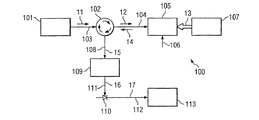
図1は、本発明の一実施形態による、遠隔の試験対象デバイスから電子計測機器へ光ファイバケーブルを介して電気応答信号の複製を伝送するシステム100を示す。図1に示す遠隔検出構成において、CW光源101から発射された連続波(CW)光ビーム11は、光サーキュレータ102を通過し、CW光ビーム12として光導波路104を通過する。CW光ビーム12は、遠隔検出点の光信号変調器、例えばREAM(反射モード電界吸収変調器)105において、遠隔の電気デバイス107によって生成された遠隔電気信号13で変調される。通常、REAM105にはバイアス電圧106が印加され、線形動作が行なわれる。次に、変調された光ビーム14はREAM105で反射され、光導波路104、光サーキュレータ102および光導波路108を通って、変調された光ビーム15として戻される。次に、変調された光ビーム15は通常、光増幅器109によって増幅され、増幅された光ビーム16として光導波路111を通して出力される。変調・増幅された光ビーム16は通常、光検出器110によって検出される。光検出器110は光電気信号17を生成し、それを電気ケーブル112を通して出力する。光電気信号17は遠隔電気信号13の複製であり、通常は電子計測機器113によって処理される。
FIG. 1 illustrates a
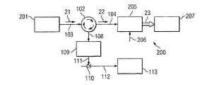
図2は、本発明の一実施形態による、遠隔の電気デバイスを刺激するための変調された信号を光ファイバ接続を介して遠隔伝送するシステム200を示す。変調信号源201からの変調された光信号21は、光ファイバリンク103および光サーキュレータ102を通過し、変調された光信号22として光ファイバリンク104を通過し、REAM(反射モード電界吸収変調器)205に入射する。REAM205は、図1に示したREAM105と同一のものでよい。REAM205は通常、負の電圧206でバイアスされ、変調された光信号22を電気信号23に変換する。電気信号23は試験対象の電気デバイス207に刺激を与える。遠隔電気デバイス207の応答は他の手段でモニタすることができ、その場合、サーキュレータ102、光増幅器109、光検出器110、電子計測計器113を使用する必要はない。それらの構成要素が描かれているのは、図2の刺激試験および図1の応答試験が、どちらも同じ装置を用いて実施できることを示すためである。両者の違いは、光源がCW光源であるか、変調光源であるかにある。
FIG. 2 illustrates a
図3は、本発明の一実施形態による、遠隔の電気デバイスに対して光ファイバリンクを介して刺激信号と応答信号の両方を双方向に同時に伝送するシステム300を示す。変調光源201からの変調された光信号21は、光ファイバ接続103および光サーキュレータ102を通過し、変調された光信号22として光ファイバ接続104を通過し、反射モード電界吸収変調器(REAM)305に入射する。REAM305は、図2に示したREAM205と同一のものでよい。REAM305は通常、線形動作させるためにバイアス電圧306によってバイアスされ、変調された光信号22を電気信号33に変換する。電気信号33は試験対象の電気デバイス307に刺激を与える。電気デバイス307は刺激(33)に応答(34)して該電気デバイス307の端子電圧を変化させ、REAM305の反射係数を変調させる。REAM305の反射係数は入射光22に相互作用し、応答電圧34の変調された複製光35は、光導波路104、光サーキュレータ102および光導波路セグメント108を通って変調された複製光36として反射される。変調された複製光36は通常、光増幅器109によって増幅され、変調・増幅された複製光16として光導波路セグメント111を通じて光検出器110に伝送され、電子計測機器113によって処理される。図3に示した構成の典型的応用形態は時間分域反射率測定(TDR)であるが、刺激/応答の他の組み合わせの応用形態を実施することもでき、例えば、ネットワーク分析(電子ネットワークの周波数領域試験)等を実施することもできる。
FIG. 3 illustrates a
頭字語「REAM」は、「反射モード電界吸収変調器」("Reflection-mode Electroabsorption Modulator")を表す。REAMは、基本的に反射モードで動作するように構成された電界吸収変調器である。REAMは、例えば変調器の第1の面に光を入射させ、変調器の反対側の面を鏡で終端することによって、反射モードで動作する。反射変調器は自由空間光ビームと共に使用され、通信システムの形成に使用される。 The acronym “REAM” stands for “Reflection-mode Electroabsorption Modulator”. A REAM is an electroabsorption modulator that is basically configured to operate in a reflective mode. The REAM operates in a reflective mode, for example by allowing light to enter the first surface of the modulator and terminating the opposite surface of the modulator with a mirror. Reflective modulators are used with free space light beams and are used to form communication systems.
光信号変調器は、電気光学変調(EOM)タイプ、電気機械変調(EMM)タイプおよび電界吸収変調(EAM)タイプなどを含む、いかなるタイプの反射モード変調器であってもよい。電気信号を変調された光に変換する電気−光変調器(EOM)や、変調された光を電気信号に変換する光検出器の使用は、多くの光通信システムで普通に実施されている。電界吸収変調器(EAM)を実施する利点は少ないが、電界吸収変調器(EAM)は、種々の変調器タイプの中でもとりわけ、光の変調器としての機能と、光の検出器としての機能とを両方とも備えている点が、特に優れているものと考えられる。 The optical signal modulator may be any type of reflection mode modulator, including electro-optic modulation (EOM) type, electromechanical modulation (EMM) type, electroabsorption modulation (EAM) type, and the like. The use of electro-optic modulators (EOM) that convert electrical signals into modulated light and photodetectors that convert modulated light into electrical signals is commonly practiced in many optical communication systems. Although there are few advantages of implementing electroabsorption modulators (EAMs), electroabsorption modulators (EAMs), among other modulator types, function as light modulators and as light detectors. It is thought that it is particularly excellent that both are provided.
図4Aは、電界吸収変調器(EAM)401を含む変調器構成400を示す。電界吸収変調器(EAM)401は、光ビームの伝送強度を印加制御電圧402に比例させるように制御する。EAM401は、左側の面から入射した光41のうちの時間変動する比率に応じた部分を変調された光42として右側の面から出射させ、その時間変動する比率を時間変動する制御電圧402によって制御し、伝送される光を変調する。図4Bは、本発明の一実施形態による反射モードEAM(REAM)410を示す。EAM(REAM)410は、EAM401に反射面403(例えば、鏡など)を結合し、入力ビーム41や変調された出力ビーム43を変調器の左側の面から入出力するように構成したものである。
FIG. 4A shows a
検出やプロービングなどの応用分野におけるREAM構造の利点は、光路を1本しか必要としない点にある。例えば光路を光ファイバにすれば、全体の組立てを非常に容易かつ簡単に行なうことができるようになる。 The advantage of the REAM structure in applications such as detection and probing is that only one optical path is required. For example, if the optical path is an optical fiber, the entire assembly can be performed very easily and simply.
図5は、本発明の一実施形態による典型的なREAMにおいて入射電力を一定にしたときの制御電圧と反射電力の関係を示す伝達曲線を示すグラフである。反射電力は、水平軸501の制御電圧の関数として、垂直軸502に沿って示されてる。バイアス電圧は、選択された特定値の制御電圧である。線形動作範囲の中央付近でデバイスをバイアスするために、電圧505のような負の直流バイアス値を印加しなければならない。これによって、平衡反射電力値504が生成される。そして、バイアス点503を中心とする線形動作が可能になる。Vbias=0でデバイスを構成することもできるが、そのようなデバイスは一般に、変調電圧の変化に対する反射応答が遅くなる。
FIG. 5 is a graph showing a transfer curve showing the relationship between the control voltage and the reflected power when the incident power is constant in a typical REAM according to an embodiment of the present invention. The reflected power is shown along the
REAMは、波長および制御電圧Vcontrolの特定の値に応じて決まる度合いで光を吸収する。通常、Vcontrolが0ボルトであるとき、REAMは「透明」であると言われ、全ての光が反射される。VcontrolをVbiasに設定すると、REAMは線形領域で動作し、反射される光の量はその印加電圧に線形比例する。このVbias値は、検出モードの動作で検出効率が最大でなくてもよいときに使用されることがある。REAMを例えばVbias=−5Vでバイアスすると、ほぼ全ての入射光が吸収される。このVbias値は、検出モードの動作で最大の検出効率および帯域が必要とされるときに使用されることがある。 REAM absorbs light to a degree that depends on the wavelength and the specific value of the control voltage Vcontrol. Normally, when Vcontrol is 0 volts, REAM is said to be “transparent” and all light is reflected. When Vcontrol is set to Vbias, the REAM operates in the linear region and the amount of reflected light is linearly proportional to the applied voltage. This Vbias value may be used when the detection efficiency does not have to be maximum in the operation in the detection mode. When REAM is biased at, for example, Vbias = −5V, almost all incident light is absorbed. This Vbias value may be used when maximum detection efficiency and bandwidth are required for detection mode operation.
Vcontrolを負の電圧に設定してREAMをバイアスすると、入射光が吸収され、入射光のエネルギーを用いて、可動電荷の「正孔−電子対」が生成される。それらの可動の正孔および電子は、REAMの電気端子から電荷の流れ(光電流)として掃き出される。この光電流の応答時間は短いため、入射光の強度が変調されると、その光を吸収することによって生成される光電流も変調され、それによって変調された光の光強度の有用な電気的複製が生成される。このような動作メカニズムは光電効果と呼ばれ、従来は光検出器に用いられていたが、これによってREAMを光検出器として使用することが可能になる。 When Vcontrol is set to a negative voltage and REAM is biased, the incident light is absorbed and a “hole-electron pair” of mobile charges is generated using the energy of the incident light. These movable holes and electrons are swept out from the electrical terminals of the REAM as a charge flow (photocurrent). Because the response time of this photocurrent is short, when the intensity of the incident light is modulated, the photocurrent generated by absorbing that light is also modulated, which makes the useful electrical intensity of the modulated light A duplicate is generated. Such an operation mechanism is called a photoelectric effect, which has been conventionally used in a photodetector, but this makes it possible to use REAM as a photodetector.
電界吸収変調器の一例の動作に関する基本的説明については、インターネット上の下記のURLから入手することができる。
http://www.bell-labs.com/project/oevlsi/tutorial/
A basic description of the operation of an example of an electroabsorption modulator can be obtained from the following URL on the Internet.
http://www.bell-labs.com/project/oevlsi/tutorial/
量子井戸内においてのみ観察される特定の電界吸収メカニズムは、「量子閉じ込めシュタルク効果」と呼ばれる。このメカニズムは、半導体における他の電界吸収メカニズムと同様に、非常に高速である。タイムスケールが1ピコ秒を遥かに下回るまで、メカニズム自体に速度制限は基本的に全く存在しない。事実上、速度制限になるのは量子井戸に電圧を印加するのに要する時間だけであり、その時間は通常、外部回路の抵抗−キャパシタンス制限によって決まる。40GHzの速度が、実証されている。 The specific electroabsorption mechanism observed only within the quantum well is called the “quantum confined Stark effect”. This mechanism is very fast, as are other electroabsorption mechanisms in semiconductors. Until the time scale is well below 1 picosecond, there is essentially no speed limit on the mechanism itself. In effect, the only speed limitation is the time required to apply a voltage to the quantum well, which is usually determined by the resistance-capacitance limitations of the external circuit. A speed of 40 GHz has been demonstrated.
図6は、電界吸収変調器(EAM)の一例である量子井戸変調器の構造600を示す。量子井戸601は、nがドープされた基板604上のpがドープされた上部接点602と、nがドープされた底部接点603との間に挟まれた、複数層の何もドープされていない半導体層である。これがダイオード構造を形成する。接点605,606を介してこのダイオード構造を逆バイアスすると、量子井戸層に対して垂直な変調された電界をかけることができる。この電界は、入力光ビーム61を変調し、変調された光ビーム62を出力させる。構造600は、波長約850nmで最も良好に動作するように、砒化ガリウムやアルミニウム砒化ガリウムを用いて製作されているが、他の半導体材料を用いることもできる。量子井戸の構造および動作に関するさらに詳しい説明は、例えばD.A.B.Miller著の「Optoelectronic applications of quantum wells」、Optics and Photonics News 1、第2号、1990年2月、pp7−15に記載されている。
FIG. 6 shows a
電気光学変調器は通常、ニオブ−タンタル酸カリウムやチタン酸バリウム等の結晶が有する二次電気光学効果(電気光学カー効果)を利用している。他の光変調器としては、二重水素リン酸カリウムや二重水素砒酸セシウム等の結晶に生じる線形電気光学効果(ポッケルス効果)を利用したものもある。電気機械変調器は、応力複屈折や光弾性の原理を利用していて、結晶の水晶等の材料を用いた音響光学変調器の類を含む。電気光学変調および電気機械変調の概要については、Hecht著の「Optics」、第2版、アディソン−ウェズリー出版社、1987年、pp.314−321に記載されている。 The electro-optic modulator normally uses the secondary electro-optic effect (electro-optic Kerr effect) possessed by crystals such as niobium-potassium tantalate and barium titanate. Other optical modulators utilize a linear electro-optic effect (Pockels effect) that occurs in crystals such as double hydrogen potassium phosphate and double hydrogen cesium arsenate. Electromechanical modulators utilize the principles of stress birefringence and photoelasticity and include a class of acousto-optic modulators using materials such as crystal quartz. For an overview of electro-optic and electromechanical modulation, see "Optics" by Hecht, 2nd edition, Addison-Wesley Publishing Company, 1987, pp. 314-321.
図7Aは、本発明の一実施形態による、線形動作を行なわせるために、入力信号に結合された交流電圧でバイアスされたREAM構造700を示す。基本的なREAMデバイス701は、電子ダイオードとして図示されている。バイアス抵抗703を通してバイアス電圧71を印加するとともに、交流結合コンデンサ702を通して電気信号72を出し入れし、電気信号72を交流電圧に結合させる。REAM701には基準電圧73が印加される。光ビーム74,75が電気信号72によって変調される。あるいは、光ビーム74,75が電気信号72を変調する。多くの電気デバイスと同様に、図5に関して説明したように、REAMは通常バイアスされる。この適当なバイアス電圧は、検出対象電圧に一致させる必要はない。多くの場合、REAMと試験対象電圧との間に交流結合が必要である。
FIG. 7A shows a
図7Bは、本発明の一実施形態による差動対REAM構造710を示す。直流結合REAMセンサを構成する一つの方法は、2つの基本的なREAMデバイス701を差動対として動作するように構成することである。各バイアス抵抗703,704を通して負のバイアス電圧71を印加するとともに、バイアス抵抗705を通して正バイアス電圧70を印加し、それらの電気信号を72,73の部分でそれぞれ接続する。信号は、変調された電圧信号であってもよいし、直流基準電圧であってもよい。光ビーム74〜77が電気信号72,73によって変調される。あるいは、光ビーム74〜77が電気信号72,73を変調する。
FIG. 7B shows a differential pair REAM
図8A〜図8Eは、REAM構造の様々な応用形態を示す。図8Aは、本発明の一実施形態によるREAM構造800を示す。REAM構造800では、信号807およびグラウンド805からの電圧が、ハウジング808内の接点プローブチップ804,806を通じてREAM801に印加される。入力光ビームおよび出力光ビーム81,82は、光ファイバ803とREAM801の間のレンズ802によって結合される。REAM構造800は、高い入力インピーダンスを有し、信号線に対して最小限の電気的負荷しか有しない。
8A-8E illustrate various applications of the REAM structure. FIG. 8A shows a
図8Bは、本発明の一実施形態によるREAM構造820を示す。REAM構造820では、ハウジング808内の非接触静電結合プローブチップ809,811を通じて、REAM801に電圧810,812が印加される。入力光ビームおよび出力光ビーム81,82は、光ファイバ803とREAM801の間のレンズ802によって結合される。REAM構造820は、高い入力インピーダンスを有し、信号線に対して最小限の電気的負荷しか有しない。
FIG. 8B shows a
図8Cは、本発明の一実施形態によるREAM構造840を示す。REAM構造840では、同軸コネクタ814に取り付けられたインピーダンス整合回路網813を通じてREAM801に電圧が印加される。入力光ビームおよび出力光ビーム81,82は、光ファイバ803とREAM801の間のレンズ802によって結合される。REAM構造840は、同軸コネクタ(通常は50オーム)と同じ負荷を有する。
FIG. 8C shows a
図8Dは、本発明の一実施形態によるREAM構造860を示す。REAM構造860は、アンテナ815の端子を通じてREAM801に電圧が印加される。従来の構成と同様に、アンテナ815は、少なくとも2つの端子を有する単一のアンテナとして構成することができる。端子の1つは接地される場合がある。整合回路網813は、REAMのインピーダンスをアンテナ815にとって最適な負荷に変換する。入力光ビームおよび出力光ビーム81,82は、光ファイバ803とREAM801の間のレンズ802によって結合される。
FIG. 8D shows a
図8Eは、本発明の一実施形態によるREAM構造880を示す。REAM構造880では、電磁波方向性結合器816を介してREAM801に電圧が印加される。この電圧は、電磁線路817上を進行する波形の振幅に比例する。入力光ビームおよび出力光ビーム81,82,83,84は、光ファイバ803とREAM801の間のレンズ802によって結合される。
FIG. 8E shows a
本発明は特定の実施形態を参照して説明されているが、当業者であれば、上記の説明から多数の代替、修正、及び変形が明らかとなるであろう。従って、本発明には、特許請求の範囲に記載される本発明の思想および範囲に含まれるようなそれらの代替、修正、及び変形もすべて含めることを意図している。 Although the present invention has been described with reference to particular embodiments, numerous alternatives, modifications, and variations will become apparent to those skilled in the art from the foregoing description. Accordingly, the present invention is intended to embrace all such alternatives, modifications and variations that fall within the spirit and scope of the present invention as set forth in the appended claims.
100、200、300 光電気システム
105、205、305 光信号変調器
104 光導波路
14、22 入力光ビーム
14、35 出力光ビーム
23 刺激信号
34 応答信号
106 バイアス電圧
113 電子計測機器
410 REAM(反射モード電界吸収変調器)
100, 200, 300
Claims (10)
前記光信号変調器に接続された入力光導波路(104)および出力光導波路(104)と、
前記入力光導波路(104)を通って入射した入力光ビーム(12)を出力光ビーム(14)として前記出力光導波路(104)を通じて反射させるように前記光信号変調器に配置された光反射要素(403)と、
前記光信号変調器(105)に設けられた電気端子(106)であって、該電気端子上の電気信号を前記入力光ビーム12と相互作用させるように構成された電気端子(106)と
からなる光電気システム(100,200,300)。 An optical signal modulator (105, 205, 305);
An input optical waveguide (104) and an output optical waveguide (104) connected to the optical signal modulator;
A light reflecting element disposed in the optical signal modulator to reflect an input light beam (12) incident through the input optical waveguide (104) as an output light beam (14) through the output optical waveguide (104). (403)
An electrical terminal (106) provided in the optical signal modulator (105), the electrical terminal (106) configured to interact an electrical signal on the electrical terminal with the input light beam 12; A photoelectric system (100, 200, 300).
光信号変調を用いて入力光ビーム(12)を電気信号(13)で変調するステップと、
変調された光ビーム(14)を出力光ビームとして前記入力光ビーム(12)の方向とは異なる方向に反射させるステップと
からなる方法。 A method for transmitting a modulated signal, comprising:
Modulating the input light beam (12) with an electrical signal (13) using optical signal modulation;
Reflecting the modulated light beam (14) as an output light beam in a direction different from the direction of the input light beam (12).
Applications Claiming Priority (1)
| Application Number | Priority Date | Filing Date | Title |
|---|---|---|---|
| US10/782,051 US7280267B2 (en) | 2004-02-19 | 2004-02-19 | Device for remotely stimulating and measuring electronic signals through a fiber optic cable |
Publications (2)
| Publication Number | Publication Date |
|---|---|
| JP2005260925A true JP2005260925A (en) | 2005-09-22 |
| JP2005260925A5 JP2005260925A5 (en) | 2008-03-27 |
Family
ID=34711858
Family Applications (1)
| Application Number | Title | Priority Date | Filing Date |
|---|---|---|---|
| JP2005031755A Pending JP2005260925A (en) | 2004-02-19 | 2005-02-08 | Device for remotely stimulating and measuring electric signals through fiber optic cable |
Country Status (4)
| Country | Link |
|---|---|
| US (1) | US7280267B2 (en) |
| EP (1) | EP1566619A2 (en) |
| JP (1) | JP2005260925A (en) |
| CN (1) | CN1658249A (en) |
Cited By (3)
| Publication number | Priority date | Publication date | Assignee | Title |
|---|---|---|---|---|
| JP2009533881A (en) * | 2006-04-18 | 2009-09-17 | パイロフォトニクス レーザーズ インコーポレイテッド | Method and system for a tunable pulsed laser source |
| KR101357719B1 (en) * | 2006-05-17 | 2014-02-03 | 에올라이트 시스템스 | High-power fiberoptic pulsed laser device |
| JP2015504280A (en) * | 2012-01-08 | 2015-02-05 | オプティウェイ リミテッド | Optical dispersion antenna system |
Families Citing this family (7)
| Publication number | Priority date | Publication date | Assignee | Title |
|---|---|---|---|---|
| KR20060025743A (en) * | 2004-09-17 | 2006-03-22 | 삼성전자주식회사 | Optical network for bi-directional wireless communication |
| US8594469B2 (en) * | 2008-12-22 | 2013-11-26 | Electronics And Telecommunications Research Institute | Optical amplifier |
| US9239348B2 (en) | 2013-03-14 | 2016-01-19 | Kirk S. Giboney | Optical modulator directional measurement system |
| GB201411342D0 (en) * | 2014-06-26 | 2014-08-13 | Rolls Royce Plc | Wireless communication system |
| CN109342807B (en) * | 2018-12-17 | 2021-08-27 | 中北大学 | Voltage sensing device combining elastic light modulation and electro-optic modulation and detection method |
| CN110233669A (en) * | 2019-07-25 | 2019-09-13 | 重庆金山医疗技术研究院有限公司 | Using the endoscopic system of illuminating light communication |
| US11874538B2 (en) * | 2020-09-30 | 2024-01-16 | Taiwan Semiconductor Manufacturing Company Limited | Apparatus and method for generating an optical signal |
Family Cites Families (6)
| Publication number | Priority date | Publication date | Assignee | Title |
|---|---|---|---|---|
| US5402234A (en) * | 1992-08-31 | 1995-03-28 | Zygo Corporation | Method and apparatus for the rapid acquisition of data in coherence scanning interferometry |
| US5402259A (en) * | 1993-04-23 | 1995-03-28 | Trw Inc. | Linear electroabsorptive modulator and related method of analog modulation of an optical carrier |
| US5898517A (en) * | 1995-08-24 | 1999-04-27 | Weis; R. Stephen | Optical fiber modulation and demodulation system |
| US5966234A (en) * | 1997-06-24 | 1999-10-12 | Lucent Technologies Inc | Retro-reflecting electroabsorption optical modulators |
| JPH11119177A (en) * | 1997-10-13 | 1999-04-30 | Oki Electric Ind Co Ltd | Light/time multiplex modulation transmitter module |
| WO2005029022A1 (en) * | 2003-09-19 | 2005-03-31 | Queen's University At Kingston | Method and apparatus for directly measuring the phase change of an optical signal |
-
2004
- 2004-02-19 US US10/782,051 patent/US7280267B2/en not_active Expired - Fee Related
- 2004-10-21 EP EP04025049A patent/EP1566619A2/en not_active Withdrawn
- 2004-11-12 CN CN200410089953.6A patent/CN1658249A/en active Pending
-
2005
- 2005-02-08 JP JP2005031755A patent/JP2005260925A/en active Pending
Cited By (4)
| Publication number | Priority date | Publication date | Assignee | Title |
|---|---|---|---|---|
| JP2009533881A (en) * | 2006-04-18 | 2009-09-17 | パイロフォトニクス レーザーズ インコーポレイテッド | Method and system for a tunable pulsed laser source |
| KR101456169B1 (en) * | 2006-04-18 | 2014-11-03 | 이에스아이-파이로포토닉스 레이저스, 인코포레이티드 | Method and system for tunable pulsed laser source |
| KR101357719B1 (en) * | 2006-05-17 | 2014-02-03 | 에올라이트 시스템스 | High-power fiberoptic pulsed laser device |
| JP2015504280A (en) * | 2012-01-08 | 2015-02-05 | オプティウェイ リミテッド | Optical dispersion antenna system |
Also Published As
| Publication number | Publication date |
|---|---|
| US7280267B2 (en) | 2007-10-09 |
| US20050185246A1 (en) | 2005-08-25 |
| EP1566619A2 (en) | 2005-08-24 |
| CN1658249A (en) | 2005-08-24 |
Similar Documents
| Publication | Publication Date | Title |
|---|---|---|
| JP2005260925A (en) | Device for remotely stimulating and measuring electric signals through fiber optic cable | |
| KR100243779B1 (en) | Electric field sensor | |
| JP2791856B2 (en) | Electric field sensor | |
| CN108844614B (en) | Chaotic Brillouin optical correlation domain analysis system and method based on phase spectrum measurement | |
| US6285182B1 (en) | Electro-optic voltage sensor | |
| US5517303A (en) | Coherence selective sensor system | |
| Masterson et al. | Photonic probes for the measurement of electromagnetic fields over broad bandwidths | |
| CN111162835A (en) | Optical time domain reflectometer | |
| Chen et al. | Photonics-Based Instantaneous Microwave Frequency Measurement System with Improved Resolution and Robust Performance | |
| Jungerman et al. | Frequency domain optical network analysis using integrated optics | |
| JP2011033501A (en) | Electric field, magnetic field and voltage detector with feedback circuit | |
| JPH0989961A (en) | Electric field detecting device | |
| Rabbani et al. | Microwave photonic IFM receiver with adjustable measurement range based on a dual-output Sagnac loop | |
| JP3180927B2 (en) | Phase fluctuation measurement device | |
| JP2014215140A (en) | Electric field measuring apparatus | |
| JPH09113557A (en) | Operating point adjusting method for electric field sensor and electric field sensor | |
| CN210867700U (en) | Optical time domain reflectometer | |
| JP2562287Y2 (en) | Electric field antenna | |
| CN115790680A (en) | Measuring system | |
| JP3355502B2 (en) | Electric field sensor | |
| JP3355503B2 (en) | Electric field sensor | |
| Li et al. | Harmonic signals from electroabsorption modulators for bias control | |
| JP3505669B2 (en) | Electric field sensor | |
| JPH052043A (en) | Electric field sensor | |
| JP3673611B2 (en) | Electric field sensor |
Legal Events
| Date | Code | Title | Description |
|---|---|---|---|
| A521 | Request for written amendment filed |
Free format text: JAPANESE INTERMEDIATE CODE: A523 Effective date: 20080207 |
|
| A621 | Written request for application examination |
Free format text: JAPANESE INTERMEDIATE CODE: A621 Effective date: 20080207 |
|
| A131 | Notification of reasons for refusal |
Free format text: JAPANESE INTERMEDIATE CODE: A131 Effective date: 20080325 |
|
| A521 | Request for written amendment filed |
Free format text: JAPANESE INTERMEDIATE CODE: A523 Effective date: 20080625 |
|
| A131 | Notification of reasons for refusal |
Free format text: JAPANESE INTERMEDIATE CODE: A131 Effective date: 20090317 |
|
| A02 | Decision of refusal |
Free format text: JAPANESE INTERMEDIATE CODE: A02 Effective date: 20090811 |