EP1564854A1 - Semiconductor light-emitting device and method for manufacturing same - Google Patents
Semiconductor light-emitting device and method for manufacturing same Download PDFInfo
- Publication number
- EP1564854A1 EP1564854A1 EP03772701A EP03772701A EP1564854A1 EP 1564854 A1 EP1564854 A1 EP 1564854A1 EP 03772701 A EP03772701 A EP 03772701A EP 03772701 A EP03772701 A EP 03772701A EP 1564854 A1 EP1564854 A1 EP 1564854A1
- Authority
- EP
- European Patent Office
- Prior art keywords
- layer
- barrier
- doped
- semiconductor light
- emitting element
- Prior art date
- Legal status (The legal status is an assumption and is not a legal conclusion. Google has not performed a legal analysis and makes no representation as to the accuracy of the status listed.)
- Granted
Links
Images



Classifications
-
- H—ELECTRICITY
- H01—ELECTRIC ELEMENTS
- H01S—DEVICES USING THE PROCESS OF LIGHT AMPLIFICATION BY STIMULATED EMISSION OF RADIATION [LASER] TO AMPLIFY OR GENERATE LIGHT; DEVICES USING STIMULATED EMISSION OF ELECTROMAGNETIC RADIATION IN WAVE RANGES OTHER THAN OPTICAL
- H01S5/00—Semiconductor lasers
- H01S5/30—Structure or shape of the active region; Materials used for the active region
- H01S5/305—Structure or shape of the active region; Materials used for the active region characterised by the doping materials used in the laser structure
-
- B—PERFORMING OPERATIONS; TRANSPORTING
- B82—NANOTECHNOLOGY
- B82Y—SPECIFIC USES OR APPLICATIONS OF NANOSTRUCTURES; MEASUREMENT OR ANALYSIS OF NANOSTRUCTURES; MANUFACTURE OR TREATMENT OF NANOSTRUCTURES
- B82Y20/00—Nanooptics, e.g. quantum optics or photonic crystals
-
- H—ELECTRICITY
- H01—ELECTRIC ELEMENTS
- H01S—DEVICES USING THE PROCESS OF LIGHT AMPLIFICATION BY STIMULATED EMISSION OF RADIATION [LASER] TO AMPLIFY OR GENERATE LIGHT; DEVICES USING STIMULATED EMISSION OF ELECTROMAGNETIC RADIATION IN WAVE RANGES OTHER THAN OPTICAL
- H01S5/00—Semiconductor lasers
- H01S5/30—Structure or shape of the active region; Materials used for the active region
- H01S5/305—Structure or shape of the active region; Materials used for the active region characterised by the doping materials used in the laser structure
- H01S5/3086—Structure or shape of the active region; Materials used for the active region characterised by the doping materials used in the laser structure doping of the active layer
-
- H—ELECTRICITY
- H01—ELECTRIC ELEMENTS
- H01S—DEVICES USING THE PROCESS OF LIGHT AMPLIFICATION BY STIMULATED EMISSION OF RADIATION [LASER] TO AMPLIFY OR GENERATE LIGHT; DEVICES USING STIMULATED EMISSION OF ELECTROMAGNETIC RADIATION IN WAVE RANGES OTHER THAN OPTICAL
- H01S5/00—Semiconductor lasers
- H01S5/30—Structure or shape of the active region; Materials used for the active region
- H01S5/34—Structure or shape of the active region; Materials used for the active region comprising quantum well or superlattice structures, e.g. single quantum well [SQW] lasers, multiple quantum well [MQW] lasers or graded index separate confinement heterostructure [GRINSCH] lasers
- H01S5/343—Structure or shape of the active region; Materials used for the active region comprising quantum well or superlattice structures, e.g. single quantum well [SQW] lasers, multiple quantum well [MQW] lasers or graded index separate confinement heterostructure [GRINSCH] lasers in AIIIBV compounds, e.g. AlGaAs-laser, InP-based laser
- H01S5/34333—Structure or shape of the active region; Materials used for the active region comprising quantum well or superlattice structures, e.g. single quantum well [SQW] lasers, multiple quantum well [MQW] lasers or graded index separate confinement heterostructure [GRINSCH] lasers in AIIIBV compounds, e.g. AlGaAs-laser, InP-based laser with a well layer based on Ga(In)N or Ga(In)P, e.g. blue laser
Definitions
- the present invention relates to a semiconductor light-emitting element.
- Semiconductor laser elements have been realized in which a quantum well layer formed by sandwiching a semiconductor layer that has a small band gap and a film thickness of a few nanometers between two semiconductor layers having larger band gaps is used as a light-emitting layer.
- Semiconductor laser elements which allow a low threshold value operation by using a modulated doped structure as the active layer of a multiple quantum well (MQW) structure have also been proposed.
- MQW multiple quantum well
- the doping of the InGaN-MQW that acts as the active layer with impurities such as Si or the like has been uniformly performed in the barrier layers alone or well layers alone or in both types of layers (for example, see Re-published Patent WO98/19375).
- MQW in which the active layer is not doped, i.e. , undoped MQW (that are not intentionally doped with impurities) have also been proposed (for example, see Japanese Patent Application Laid-Open No. 2001-7444).
- the semiconductor light-emitting element of the present invention is a semiconductor light-emitting element composed of at least compound semiconductors comprising an active layer consisting of a quantum well structure including a well layer and barrier layers between which said well layer is sandwiched, wherein said well layer has in part a doped well region to which an n-type impurity is added at the interface with said barrier layer on an electron injection side and in the vicinity of said interface, and wherein said barrier layer has a doped barrier region to which said n-type impurity is added at least at said interface and in the vicinity of said interface.
- the semiconductor light emitting element manufacturing method of the present invention is a method for manufacturing a semiconductor light-emitting element composed of at least compound semiconductors including an active layer consisting of a quantum well structure having a well layer and barrier layers betweenwhich saidwell layer is sandwiched, saidmethod comprising the steps of: growing a barrier layer while adding an n-type impurity so that a doped barrier region to which said n-type impurity is added is formed to the uppermost surface; and growing a well layer on said uppermost surface of the barrier layer while adding said n-type impurity to form a doped well region to which said n-type impurity is added on said uppermost surface servicing as an interface with said barrier layers on the electron injection side.
- FIG. 1 shows a group III nitride semiconductor laser element of one embodiment.
- This semiconductor laser element comprises: an n-type contact layer 3; an n-type cladding layer 4; an n-type guide layer 5; an active layer 6 with a quantum well structure consisting of one or a plurality of pairs of well layers and barrier layers whose major constituent elements are In, Ga and N; a p-type guide layer 8; a p-type cladding layer 9; and a p-type contact layer 10 which are laminated in that order on a single-crystal sapphire substrate 1.
- an n-type electrode 14 and a p-type electrode 13 of the semiconductor laser element are respectively connected to the n-type contact layer 3 and p-type contact layer 10.
- this semiconductor laser element is composed of p-type and n-type carrier injection layer groups which are positioned above and below the active layer with the quantum well structure made of at least group III nitride, and which inject holes and electrons into the active layer respectively.
- Each of the two carrier injection layer groups comprises the guide layer, the cladding layer and the contact layer which are disposed in the order on either side of the active layer.
- a ridge stripe part 18 is formed in the p-type cladding layer 9, and the element is covered and protected by a SiO 2 insulating film 11 except for the electrodes.
- the n-type and p-type cladding layers 4 and 9 are formed to have refractive indexes lower than those of the n-type and p-type guide layers 5 and 8, so that generated light-waves are guided in the direction of the film thickness by virtue of the difference in refractive index with the guide layers.
- the ridge stripe part 18 generates a horizontal step in the effective refractive index by varying the film thickness of the cladding layer 9, and is provided in order to confine the generated light in the horizontal direction.
- the n-type contact layer 3 is an underlayer provided as a current path. The layer 3 is provided since sapphire serving as the substrate does not have any electric conductivity at all.
- a so-called buffer layer made of GaN or AlN formed at a low temperature may also be disposed between the n-type contact layer 3 and the sapphire substrate 1.
- an electron barrier layer made of p-type AlGaN may also be disposed between the active layer 6 and the p-type guide layer 8, in particular, to further enhance the confinement of electrons.
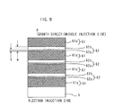
- the active layer 6 of the group III nitride semiconductor laser element has a compound semiconductor quantum well structure comprising well layers 62 each partially doped with Si, and adjacent Si-doped barrier layers 61 which are layered alternately.
- the injected electrons are collected mainly in the well layers 62.
- the active layer consists of well layers 62 that have a high In content (i.e., a small band gap) and barrier layers 61 that have a low In content (i.e., a large band gap).
- the holes injected from the p-type guide layer 8 recombine with the electrons injected from the n-type guide layer 5 so that light is generated.
- the generated light is limited by the guide layers, cladding layers and ridge. The light is confined into the inside area between the pair of cladding layers, and is guided in the direction parallel to the ridge, so that this light is emitted from the end surface of the laser element.
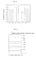
- each well layer 62 partially has a doped well region 62a to which an n-type impurity is added at the interface with the barrier layer 61 on the electron injection side and in the vicinity of this interface.
- each barrier layer 61 has a doped barrier region 61a to which an n-type impurity is added, at least at the interface and in the vicinity of this interface.
- the doped well region 62a to which an n-type impurity is added and the doped barrier region 61a to which an n-type impurity is added residing in the each adjacent set of well layer 62 and barrier layer 61 improve the light emission characteristics of the group III nitride semiconductor laser element.
- each barrier layer 61 have an undoped barrier region 61b to which no n-type impurity is added at the interface on the position hole injection side of the well layer 62, and in the vicinity of this interface.
- each well layer 62 have an undoped well region 62b to which no n-type impurity is added at the interface on the hole injection side of the well layer 62, and in the vicinity of this interface.
- n-type Group III compound semiconductor layer a Group IV or Group VI element such as Si, Ge, Se, Te or C can be used as an n-type impurity and a desirable n-type impurity is Si or Ge.
- a portion of Group III elements of the Group III nitride compound semiconductor boron (B) may be replaced with thallium (Tl).
- the substrate may be formed of silicon (Si), silicon carbide (SiC), spinel (MgAl 2 O 4 ), ZnO, MgO, etc.
- the crystalline structure of the semiconductor layer including the active layer in the present invention is a wurtzite structure, and the principal plane of the element is the so-called C plane.
- a wurtzite structure does not show mirror image symmetry with respect to the direction of the C axis, so that two (front and back) polarities, i.e., a (0001) plane and a (000-1) plane exist in the so-called C plane.
- a ⁇ 0001> direction and a ⁇ 000-1> direction also exist in the epitaxial growth direction.
- the epitaxial growth direction is the ⁇ 0001> direction. The reason for this is that it has been experimentally demonstrated that the light-emitting properties of crystal layers grown in the ⁇ 0001> direction are superior to those of crystal layers grown in the ⁇ 000-1> direction.
- an epitaxial growth of metal organic chemical vapor deposition (MOCVD) is used as the film formation method.
- MOCVD metal organic chemical vapor deposition
- the semiconductor light-emitting element can also be manufactured using a molecular beam epitaxy (MBE) method by which a steep hetero-interface can be formed.
- MBE molecular beam epitaxy
- An underlying wafer on which a GaN film with a film thickness of 15 ⁇ m has been formed beforehand as an n-type contact layer on a sapphire substrate is mounted in an MOCVD reactor, and elevation of the temperature is initiated in a hydrogen carrier gas at a pressure of 300 Torr.
- a hydrogen carrier gas at a pressure of 300 Torr.
- ammonia (NH 3 ) for a nitrogen source is introduced into the reactor, and the temperature elevation is continued.
- TMG trimethylgallium
- TMA trimethylaluminum
- MeSiH 3 methylsilane so-called MeSiH 3 for a Si precursor
- n-type guide layer consisting of Si-doped GaN is grown to a film thickness of 0.05 ⁇ m on the surface of the n-type cladding layer (n-type guide layer formation process).
- the supply of TMG and methylsilane is stopped, and a temperature drop is initiated.
- TMG and a first trimethylindium (hereinafter abbreviated as TMI) for an In precursor are introduced, and a barrier layer consisting of undoped InGaN is grown to a film thickness of 10 angstroms on the surface of the n-type guide layer (undoped barrier layer formation process).
- Si-doped region consisting of Si-doped InGaN is grown to a film thickness of 50 angstroms on top of the undoped barrier region (undoped portion) (Si-doped barrier layer formation process).
- the supply of the first TMI is stopped, and a second TMI is supplied instead, so that a doped well region (Si doped portion) consisting of Si-doped InGaN is grown to a film thickness of 10 angstroms on top of the doped barrier region (Si doped portion) (Si-doped well layer formation process).
- the only difference between the first TMI and the second TMI is the flow rate.
- a well layer (undoped portion) is grown to a film thickness of 20 angstroms on top of the doped well region (Si-doped portion) (undoped well layer formation process).
- the supply of the second TMI is stopped, and the first TMI is supplied instead, so that the process is repeated from the above-mentioned undoped barrier layer formation process.
- the process extending from the undoped barrier layer formation process to the undoped well layer formation process is repeated a total of three times.
- the final barrier layer (consisting of the undoped portion and the Si-doped portion) is formed, thus obtaining an MQW active layer of three well layers by the offset doping.
- the concentration of Si atoms in the crystal in each doping region is preferably 8E17 to 1E19/cc, and is even more preferably 1E18 to 7E18/cc.
- the flow rate of methylsilane in the above-mentioned process is adjusted so that the concentration of Si atoms in the final crystal is in the above-mentioned range.
- the film thickness of the final barrier layer reaches a total of 60 angstroms
- the supply of the first TMI and methylsilane is stopped, and TMA and bis-ethylcyclopentadienylmagnesium ⁇ Mg(C 2 H 5 C 5 H 4 ) 2 hereinafter abbreviated as EtCp2Mg ⁇ , which is a Mg precursor, are introduced instead, so that an electron barrier layer consisting of Mg-doped AlGaN is grown to a film thickness of 200 angstroms on top of the active layer (electron barrier layer formation process).
- the carrier gas is changed from nitrogen to hydrogen, and a temperature elevation is initiated.
- the substrate temperature reaches 1050 °C
- TMG and EtCp2Mg are introduced, and a p-type guide layer consisting of Mg-doped GaN is grown to a film thickness of 0.05 ⁇ m on top of the electron barrier layer (p-type guide layer formation process).
- TMA is introduced, and a p-type cladding layer consisting of Mg-doped AlGaN is grown to a film thickness of 0.5 ⁇ m on top of the p-type guide layer (p-type cladding layer formation process).
- a p-type contact layer consisting of Mg-doped GaN is grown to a film thickness of 0.1 ⁇ m on top of the p-type cladding layer (p-type contact layer formation process).
- the supply of TMG and EtCp2Mg is stopped, and a temperature drop is initiated.
- the substrate temperature reaches 400 °C or less, the supply of ammonia is stopped.
- the substrate temperature reaches room temperature, the wafer on which the semiconductor laser structure has been laminated is removed from the MOCVD apparatus.
- n-type contact layer and p-type contact layer are demarcated by partially exposing the n-type contact layer by an ordinary photolithographic process and dry etching. Furthermore, a ridge stripe part consisting of the p-type contact layer and p-type cladding layer is formed, and an insulating film consisting of SiO 2 or the like is deposited on the exposed surface. Next, windows used for the formation of electrodes are patterned in this insulating film. Then, an n-type electrode and p-type electrode consisting of titanium and nickel or the like are respectively connected to the n-type contact layer and p-type contact layer.
- the sapphire substrate side on the back surface is polished to a specified wafer thickness, and the wafer is split by cleaving so that chips are formed.
- a laser element with a ridge width of 5 ⁇ m and a resonator length of 1 mm was manufactured, and this laser element was subjected to a driving test.
- this laser element showed a laser oscillation at a wavelength of 405 nm and a threshold current density of 4.3 kA/cm 2 .
- a conventional laser element in which uniform doping was performed only in the barrier layers without any offset was also manufactured, and was subjected to a driving test.
- the threshold current density was 7.8 kA/cm 2 .
- various PL (photoluminescence) evaluation samples were manufactured in order to compare only the active layers, and measurements were performed on these samples.
- the above-mentioned samples were basically samples in which growth was halted at the uppermost barrier layer of the above-mentioned laser structure. Such samples will be referred to as MQW samples below.
- the first MQW sample had the same construction as the active layer portion of the above-mentioned laser element in the above-mentioned embodiment.
- This sample was manufactured as follows: the introduction of the first TMI and the introduction of methylsilane were not simultaneously performed in the undoped barrier layer formation process and well layer formation process, so that there was a time difference in the offset (corresponding to a film thickness of t for the doped well region equal to 1/3 of the well layer film thickness w).
- sample D This MQW sample will be referred to as sample D.
- a so-called barrier uniformly doped MQW sample was manufactured by the same process as in the case of sample D, except that methylsilane was not introduced during the growth of the well layers in the manufacturing process of sample D, and methylsilane was introduced during the growth of the barrier layers.
- a so-called well uniformly doped MQW sample was manufactured by the same process as in the case of sample D, except that methylsilane was not introduced during the growth of the barrier layers in the manufacturing process of sample D, and methylsilane was introduced during the growth of the well layers. Furthermore, the actual amount of offset was confirmed by SIMS (secondary ion mass spectroscopy analysis). In cases where methylsilane was introduced only during the growth of the barrier layers, the variations in the In profile and Si profile which serve as indicators for the well layers and barrier layers were completely matched in reverse phases. On the other hand, in cases where offset doping was performed, it was confirmed that the amount of offset corresponded to the supply timing of the precursor gases by the amounts of shift in the In profile and Si profile in SIMS analysis.
- sample E an MQW sample with so-called reverse offset doping was manufactured by the same process as the manufacturing process of sample D, except that a Si-doped portion was formed with an offset straddling the interfaces of the well layers with the barrier layers on the hole injection side.
- the introduction of the first TMI and the introduction of methylsilane were not performed simultaneously in the undoped barrier layer formation process and well layer formation process, and the sample was manufactured with an offset time difference (corresponding to -1/3 the thickness of the well layers) provided.
- an MQW sample with so-called offset doping was manufactured by the same process as the manufacturing process of sample D, except that the Si-doped portions were formed with an increased amount of offset straddling the interfaces of the well layers with the barrier layers on the electron injection side.
- the amount of offset corresponded to 2/3 of the well layer thickness.
- sample I an MQW sample with so-called one-sided offset doping was manufactured by the same process as the manufacturing process of sample D, except that the Si-doped portions were formed with an offset straddling the interfaces of the well layers with the barrier layers on the electron injection side, and all of the barrier layers were doped with Si.
- the sample E with reverse offset shows a drop in intensity even with respect to Comparative Example B, it is seen that the direction of the offset is important, and further that it is desirable that every well layer has a doped well region to which an n-type impurity is added residing in part at each interface with the barrier layer on the electron injection side, and in the vicinity of the interface, and that the barrier layers have the doped barrier regions to each of which an n-type impurity is added existing at least at the interfaces on the hole injection side and in the vicinity of these interfaces respectively.
- the film thickness of the barrier undoped layer 61b of the barrier layer 61 is equal to or less than the film thickness of the dopedwell region 62a. It is seen from the results obtained for samples D and I that it is desirable that the film thickness t of the doped well region 62a is in the range of 0 ⁇ t ⁇ (w/2), where w is the film thickness of the well layers 62.
Landscapes
- Physics & Mathematics (AREA)
- Nanotechnology (AREA)
- Engineering & Computer Science (AREA)
- Chemical & Material Sciences (AREA)
- Optics & Photonics (AREA)
- Biophysics (AREA)
- Life Sciences & Earth Sciences (AREA)
- Electromagnetism (AREA)
- General Physics & Mathematics (AREA)
- Crystallography & Structural Chemistry (AREA)
- Condensed Matter Physics & Semiconductors (AREA)
- Semiconductor Lasers (AREA)
- Led Devices (AREA)
Abstract
Description
Claims (18)
- A semiconductor light-emitting element composed of at least compound semiconductors comprising an active layer consisting of a quantum well structure including a well layer and barrier layers between which said well layer is sandwiched, wherein said well layer has in part a doped well region to which an n-type impurity is added at the interface with said barrier layer on an electron injection side and in the vicinity of said interface, and wherein said barrier layer has a doped barrier region to which said n-type impurity is added at least at said interface and in the vicinity of said interface.
- The semiconductor light-emitting element according to claim 1, wherein the film thickness t of said doped well region is in the range of 0 < t < (w/2), where w is the film thickness of said well layer.
- The semiconductor light-emitting element according to claim 1 or 2, wherein said barrier layer has an undoped barrier region to which said n-type impurity is not added at the interface with said well layer on the hole injection side, and in the vicinity of said interface.
- The semiconductor light-emitting element according to claim 3, wherein the film thickness of said undoped barrier region of said barrier layer is equal to or less than the film thickness of said doped well region.
- The semiconductor light-emitting element according to claim 1 or 2, wherein said doped barrier region spreads throughout said entire barrier layer.
- The semiconductor light-emitting element according to any one of claims 1-5, wherein the crystalline structure of said active layer is a wurtzite structure, and the principal plane of said active layer is the (0001) plane.
- The semiconductor light-emitting element according to any one of claims 1-6, wherein said compound semiconductor consists mainly of a group III nitride Bx'AlxGayInzN (x' + x + y + z = 1).
- The semiconductor light-emitting element according to any one of claims 1-7, wherein said n-type impurity is Si or Ge.
- The semiconductor light-emitting element according to any one of claims 1-8, wherein the concentrations of the n-type impurity in said doped well region and said doped barrier region are 8E17/cc to 1E19/cc respectively.
- A method for manufacturing a semiconductor light-emitting element composed of at least compound semiconductors including an active layer consisting of a quantum well structure having a well layer and barrier layers between which said well layer is sandwiched, said method comprising the steps of :growing a barrier layer while adding an n-type impurity so that a doped barrier region to which said n-type impurity is added is formed to the uppermost surface; andgrowing a well layer on said uppermost surface of the barrier layer while adding said n-type impurity to form a doped well region to which said n-type impurity is added on said uppermost surface servicing as an interface with said barrier layer on the electron injection side.
- The semiconductor light-emitting element manufacturing method according to claim 10, where the film thickness t of said doped well regions is in the range of 0 < t < (w/2), where w is the film thickness of said well layer.
- The semiconductor light-emitting element manufacturing method according to claim 10 or 11, wherein said barrier layer growing step includes a step in which undoped barrier regions to which said n-type impurity is not added are formed at the interfaces with said well layer on the hole injection side, and in the vicinity of these interfaces.
- The semiconductor light-emitting element manufacturing method according to claim 12, wherein the film thickness of said undoped barrier region of said barrier layer is equal to or less than the film thickness of said doped well region.
- The semiconductor light-emitting element manufacturing method according to claim 10 or 11, wherein said doped barrier region is formed throughout said entire barrier layers in said step in which said doped barrier region is formed.
- The semiconductor light-emitting element manufacturing method according to any one of claims 10-14, wherein said doped barrier region is formed so that the crystalline structure of said active layer is a wurtzite structure, and so that the principal plane of said active layer is the (0001) plane, in said step in which said doped barrier region is formed.
- The semiconductor light-emitting element manufacturing method according to any one of claims 10-15, wherein said compound semiconductor consists mainly of a group III nitride Bx'AlxGayInzN (x' + x + y + z = 1).
- The semiconductor light-emitting element manufacturing method according to any one of claims 10-16, wherein said n-type impurity is Si or Ge.
- The semiconductor light-emitting element manufacturing method according to any one of claims 10-17, wherein the concentrations of the n-type impurity in said doped well region and doped barrier region are 8E17/cc to 1E19/cc respectively.
Applications Claiming Priority (3)
| Application Number | Priority Date | Filing Date | Title |
|---|---|---|---|
| JP2002333168 | 2002-11-18 | ||
| JP2002333168 | 2002-11-18 | ||
| PCT/JP2003/014366 WO2004047245A1 (en) | 2002-11-18 | 2003-11-12 | Semiconductor light-emitting device and method for manufacturing same |
Publications (3)
| Publication Number | Publication Date |
|---|---|
| EP1564854A1 true EP1564854A1 (en) | 2005-08-17 |
| EP1564854A4 EP1564854A4 (en) | 2006-02-08 |
| EP1564854B1 EP1564854B1 (en) | 2007-05-09 |
Family
ID=32321686
Family Applications (1)
| Application Number | Title | Priority Date | Filing Date |
|---|---|---|---|
| EP03772701A Expired - Lifetime EP1564854B1 (en) | 2002-11-18 | 2003-11-12 | Semiconductor light-emitting device and method for manufacturing the same |
Country Status (8)
| Country | Link |
|---|---|
| US (1) | US7312468B2 (en) |
| EP (1) | EP1564854B1 (en) |
| JP (1) | JP4074290B2 (en) |
| CN (1) | CN100365891C (en) |
| AU (1) | AU2003280742A1 (en) |
| DE (1) | DE60313797T2 (en) |
| TW (1) | TWI234915B (en) |
| WO (1) | WO2004047245A1 (en) |
Cited By (2)
| Publication number | Priority date | Publication date | Assignee | Title |
|---|---|---|---|---|
| WO2009039830A1 (en) * | 2007-09-26 | 2009-04-02 | Osram Opto Semiconductors Gmbh | Optoelectronic semiconductor chip having a multiple quantum well structure |
| EP2009707A3 (en) * | 2007-06-25 | 2012-07-25 | Seoul Opto Device Co., Ltd. | Light emitting diode and method for manufacturing the same |
Families Citing this family (21)
| Publication number | Priority date | Publication date | Assignee | Title |
|---|---|---|---|---|
| US7115908B2 (en) * | 2004-01-30 | 2006-10-03 | Philips Lumileds Lighting Company, Llc | III-nitride light emitting device with reduced polarization fields |
| KR100765004B1 (en) * | 2004-12-23 | 2007-10-09 | 엘지이노텍 주식회사 | Nitride semiconductor light emitting device and manufacturing method |
| TWI282636B (en) * | 2005-12-29 | 2007-06-11 | Epistar Corp | Semiconductor light-emitting device and manufacturing method thereof |
| JP4905125B2 (en) * | 2006-01-26 | 2012-03-28 | 日亜化学工業株式会社 | Nitride semiconductor laser device and manufacturing method thereof |
| JP4884826B2 (en) * | 2006-04-28 | 2012-02-29 | ローム株式会社 | Semiconductor light emitting device |
| JP5084837B2 (en) * | 2006-10-18 | 2012-11-28 | ナイテック インコーポレイテッド | Deep ultraviolet light emitting device and method for manufacturing the same |
| JP2009212336A (en) * | 2008-03-05 | 2009-09-17 | Mitsubishi Electric Corp | Method of manufacturing nitride-based semiconductor laser, and nitride-based semiconductor laser |
| US7902545B2 (en) * | 2008-05-14 | 2011-03-08 | Baker Hughes Incorporated | Semiconductor for use in harsh environments |
| JP5191843B2 (en) | 2008-09-09 | 2013-05-08 | 株式会社東芝 | Semiconductor light emitting device and wafer |
| US8704252B2 (en) * | 2008-10-23 | 2014-04-22 | Epistar Corporation | Light emitting device |
| WO2011027417A1 (en) | 2009-09-01 | 2011-03-10 | 株式会社 東芝 | Semiconductor light emitting element |
| CN102104094B (en) * | 2009-12-21 | 2013-08-21 | 晶元光电股份有限公司 | Light emitting element and manufacturing method thereof |
| JP5636773B2 (en) * | 2010-07-06 | 2014-12-10 | ソニー株式会社 | Semiconductor laser |
| JP5135465B2 (en) * | 2011-11-29 | 2013-02-06 | 株式会社東芝 | Semiconductor light emitting device and manufacturing method thereof |
| JP5458162B2 (en) * | 2012-11-07 | 2014-04-02 | 株式会社東芝 | Semiconductor light emitting device |
| JP2014157852A (en) * | 2013-02-14 | 2014-08-28 | Toyoda Gosei Co Ltd | Group iii nitride semiconductor light-emitting element and manufacturing method of the same |
| DE102015114478A1 (en) * | 2015-08-31 | 2017-03-02 | Osram Opto Semiconductors Gmbh | Optoelectronic semiconductor chip and method for its production |
| US11417523B2 (en) | 2018-01-29 | 2022-08-16 | Northwestern University | Amphoteric p-type and n-type doping of group III-VI semiconductors with group-IV atoms |
| JP6968122B2 (en) * | 2019-06-06 | 2021-11-17 | 日機装株式会社 | Nitride semiconductor light emitting device |
| US20220190560A1 (en) * | 2020-12-15 | 2022-06-16 | Marvell Asia Pte, Ltd. | Gain medium structure for semiconductor optical amplifier with high saturation power |
| CN113410348B (en) * | 2021-06-15 | 2022-11-18 | 厦门士兰明镓化合物半导体有限公司 | Deep ultraviolet light-emitting element and preparation method thereof |
Family Cites Families (16)
| Publication number | Priority date | Publication date | Assignee | Title |
|---|---|---|---|---|
| JP3307669B2 (en) * | 1992-04-06 | 2002-07-24 | 日本電信電話株式会社 | Compound semiconductor superlattice |
| JP3976294B2 (en) * | 1998-06-26 | 2007-09-12 | シャープ株式会社 | Method for manufacturing nitride-based compound semiconductor light-emitting device |
| JP2000261106A (en) * | 1999-01-07 | 2000-09-22 | Matsushita Electric Ind Co Ltd | Semiconductor light emitting device, method of manufacturing the same, and optical disk device |
| JP2000277868A (en) * | 1999-03-25 | 2000-10-06 | Sanyo Electric Co Ltd | Light emitting element |
| JP3438648B2 (en) * | 1999-05-17 | 2003-08-18 | 松下電器産業株式会社 | Nitride semiconductor device |
| JP3511372B2 (en) * | 1999-08-31 | 2004-03-29 | シャープ株式会社 | Semiconductor light emitting device and display device using the same |
| JP2001077417A (en) * | 1999-08-31 | 2001-03-23 | Sharp Corp | Method for manufacturing nitrogen compound semiconductor light emitting device |
| US6803596B2 (en) * | 1999-12-27 | 2004-10-12 | Sanyo Electric Co., Ltd. | Light emitting device |
| JP2001267693A (en) * | 2000-03-17 | 2001-09-28 | Sanyo Electric Co Ltd | Semiconductor laser element |
| US6586762B2 (en) * | 2000-07-07 | 2003-07-01 | Nichia Corporation | Nitride semiconductor device with improved lifetime and high output power |
| JP4867064B2 (en) * | 2000-11-17 | 2012-02-01 | 住友化学株式会社 | Group 3-5 compound semiconductor for light emitting device and method for producing the same |
| JP4468600B2 (en) * | 2001-02-20 | 2010-05-26 | 富士通株式会社 | Photodetector with dark current reduction mechanism |
| US6649942B2 (en) * | 2001-05-23 | 2003-11-18 | Sanyo Electric Co., Ltd. | Nitride-based semiconductor light-emitting device |
| US6835962B2 (en) * | 2001-08-01 | 2004-12-28 | Showa Denko Kabushiki Kaisha | Stacked layer structure, light-emitting device, lamp, and light source unit |
| US6833564B2 (en) * | 2001-11-02 | 2004-12-21 | Lumileds Lighting U.S., Llc | Indium gallium nitride separate confinement heterostructure light emitting devices |
| US6665329B1 (en) * | 2002-06-06 | 2003-12-16 | Sandia Corporation | Broadband visible light source based on AllnGaN light emitting diodes |
-
2003
- 2003-11-06 TW TW092131094A patent/TWI234915B/en not_active IP Right Cessation
- 2003-11-12 AU AU2003280742A patent/AU2003280742A1/en not_active Abandoned
- 2003-11-12 JP JP2004553157A patent/JP4074290B2/en not_active Expired - Fee Related
- 2003-11-12 CN CNB2003801035898A patent/CN100365891C/en not_active Expired - Fee Related
- 2003-11-12 WO PCT/JP2003/014366 patent/WO2004047245A1/en not_active Ceased
- 2003-11-12 US US10/535,175 patent/US7312468B2/en not_active Expired - Fee Related
- 2003-11-12 DE DE60313797T patent/DE60313797T2/en not_active Expired - Lifetime
- 2003-11-12 EP EP03772701A patent/EP1564854B1/en not_active Expired - Lifetime
Cited By (3)
| Publication number | Priority date | Publication date | Assignee | Title |
|---|---|---|---|---|
| EP2009707A3 (en) * | 2007-06-25 | 2012-07-25 | Seoul Opto Device Co., Ltd. | Light emitting diode and method for manufacturing the same |
| WO2009039830A1 (en) * | 2007-09-26 | 2009-04-02 | Osram Opto Semiconductors Gmbh | Optoelectronic semiconductor chip having a multiple quantum well structure |
| US8173991B2 (en) | 2007-09-26 | 2012-05-08 | Osram Opto Semiconductors Gmbh | Optoelectronic semiconductor chip having a multiple quantum well structure |
Also Published As
| Publication number | Publication date |
|---|---|
| CN1714487A (en) | 2005-12-28 |
| TWI234915B (en) | 2005-06-21 |
| AU2003280742A1 (en) | 2004-06-15 |
| JPWO2004047245A1 (en) | 2006-03-23 |
| US20060027814A1 (en) | 2006-02-09 |
| DE60313797T2 (en) | 2008-01-24 |
| US7312468B2 (en) | 2007-12-25 |
| EP1564854B1 (en) | 2007-05-09 |
| DE60313797D1 (en) | 2007-06-21 |
| WO2004047245A1 (en) | 2004-06-03 |
| CN100365891C (en) | 2008-01-30 |
| JP4074290B2 (en) | 2008-04-09 |
| EP1564854A4 (en) | 2006-02-08 |
| TW200414643A (en) | 2004-08-01 |
Similar Documents
| Publication | Publication Date | Title |
|---|---|---|
| EP1564854B1 (en) | Semiconductor light-emitting device and method for manufacturing the same | |
| US6734530B2 (en) | GaN-based compound semiconductor EPI-wafer and semiconductor element using the same | |
| JP5434882B2 (en) | GaN-based III-V compound semiconductor light emitting device | |
| US8124432B2 (en) | Nitride semiconductor optical element and manufacturing method thereof | |
| KR100906760B1 (en) | Nitride semiconductor devices | |
| KR100267839B1 (en) | Nitride semiconductor devices | |
| EP1394912B1 (en) | Nitride semiconductor laser | |
| EP2164115A1 (en) | Nitride semiconductor light emitting element and method for manufacturing nitride semiconductor | |
| US6677617B2 (en) | Semiconductor LED composed of group III nitrided emission and fluorescent layers | |
| JP2003115642A (en) | Nitride semiconductor device | |
| KR20030064629A (en) | Semiconductor light emitting device and its manufacturing method | |
| KR20080075212A (en) | Gallium nitride semiconductor light emitting device | |
| US20060060833A1 (en) | Radiation-emitting optoelectronic component with a quantum well structure and method for producing it | |
| EP2455989A1 (en) | Nitride-based semiconductor light-emitting element | |
| US6631149B1 (en) | Laser diode using group III nitride group compound semiconductor | |
| KR100545999B1 (en) | Nitride Semiconductor Device | |
| EP1553669A1 (en) | Group iii nitride semiconductor light-emitting device and method for manufacturing same | |
| JP4178807B2 (en) | Semiconductor light emitting device and manufacturing method thereof | |
| JP4631214B2 (en) | Manufacturing method of nitride semiconductor film | |
| KR100742989B1 (en) | Method of manufacturing gallium nitride based light emitting device | |
| JPWO2005022711A1 (en) | Nitride semiconductor light emitting device and manufacturing method thereof | |
| JP2002151797A5 (en) | ||
| JP2004072044A (en) | Manufacturing method of GaN based semiconductor light emitting device | |
| HK1118962A (en) | Semiconductor laser and method for fabricating the same |
Legal Events
| Date | Code | Title | Description |
|---|---|---|---|
| PUAI | Public reference made under article 153(3) epc to a published international application that has entered the european phase |
Free format text: ORIGINAL CODE: 0009012 |
|
| 17P | Request for examination filed |
Effective date: 20050512 |
|
| AK | Designated contracting states |
Kind code of ref document: A1 Designated state(s): AT BE BG CH CY CZ DE DK EE ES FI FR GB GR HU IE IT LI LU MC NL PT RO SE SI SK TR |
|
| AX | Request for extension of the european patent |
Extension state: AL LT LV MK |
|
| A4 | Supplementary search report drawn up and despatched |
Effective date: 20051223 |
|
| DAX | Request for extension of the european patent (deleted) | ||
| RBV | Designated contracting states (corrected) |
Designated state(s): DE FR GB |
|
| RTI1 | Title (correction) |
Free format text: SEMICONDUCTOR LIGHT-EMITTING DEVICE AND METHOD FOR MANUFACTURING THE SAME |
|
| GRAP | Despatch of communication of intention to grant a patent |
Free format text: ORIGINAL CODE: EPIDOSNIGR1 |
|
| GRAS | Grant fee paid |
Free format text: ORIGINAL CODE: EPIDOSNIGR3 |
|
| GRAA | (expected) grant |
Free format text: ORIGINAL CODE: 0009210 |
|
| AK | Designated contracting states |
Kind code of ref document: B1 Designated state(s): DE FR GB |
|
| REG | Reference to a national code |
Ref country code: GB Ref legal event code: FG4D |
|
| REF | Corresponds to: |
Ref document number: 60313797 Country of ref document: DE Date of ref document: 20070621 Kind code of ref document: P |
|
| REG | Reference to a national code |
Ref country code: GB Ref legal event code: 746 Effective date: 20071007 |
|
| ET | Fr: translation filed | ||
| PLBE | No opposition filed within time limit |
Free format text: ORIGINAL CODE: 0009261 |
|
| STAA | Information on the status of an ep patent application or granted ep patent |
Free format text: STATUS: NO OPPOSITION FILED WITHIN TIME LIMIT |
|
| 26N | No opposition filed |
Effective date: 20080212 |
|
| PGFP | Annual fee paid to national office [announced via postgrant information from national office to epo] |
Ref country code: DE Payment date: 20101110 Year of fee payment: 8 |
|
| PGFP | Annual fee paid to national office [announced via postgrant information from national office to epo] |
Ref country code: GB Payment date: 20101110 Year of fee payment: 8 |
|
| PGFP | Annual fee paid to national office [announced via postgrant information from national office to epo] |
Ref country code: FR Payment date: 20111118 Year of fee payment: 9 |
|
| GBPC | Gb: european patent ceased through non-payment of renewal fee |
Effective date: 20121112 |
|
| REG | Reference to a national code |
Ref country code: FR Ref legal event code: ST Effective date: 20130731 |
|
| REG | Reference to a national code |
Ref country code: DE Ref legal event code: R119 Ref document number: 60313797 Country of ref document: DE Effective date: 20130601 |
|
| PG25 | Lapsed in a contracting state [announced via postgrant information from national office to epo] |
Ref country code: DE Free format text: LAPSE BECAUSE OF NON-PAYMENT OF DUE FEES Effective date: 20130601 |
|
| PG25 | Lapsed in a contracting state [announced via postgrant information from national office to epo] |
Ref country code: FR Free format text: LAPSE BECAUSE OF NON-PAYMENT OF DUE FEES Effective date: 20121130 Ref country code: GB Free format text: LAPSE BECAUSE OF NON-PAYMENT OF DUE FEES Effective date: 20121112 |