EP1564813A2 - Solid state imaging device with increased vertical resolution in interlace scanning method - Google Patents
Solid state imaging device with increased vertical resolution in interlace scanning method Download PDFInfo
- Publication number
- EP1564813A2 EP1564813A2 EP05003091A EP05003091A EP1564813A2 EP 1564813 A2 EP1564813 A2 EP 1564813A2 EP 05003091 A EP05003091 A EP 05003091A EP 05003091 A EP05003091 A EP 05003091A EP 1564813 A2 EP1564813 A2 EP 1564813A2
- Authority
- EP
- European Patent Office
- Prior art keywords
- state imaging
- solid state
- imaging device
- lines
- photoelectric conversion
- Prior art date
- Legal status (The legal status is an assumption and is not a legal conclusion. Google has not performed a legal analysis and makes no representation as to the accuracy of the status listed.)
- Withdrawn
Links
- 238000003384 imaging method Methods 0.000 title claims abstract description 55
- 239000007787 solid Substances 0.000 title claims abstract description 53
- 238000000034 method Methods 0.000 title description 10
- 238000006243 chemical reaction Methods 0.000 claims abstract description 47
- 239000004065 semiconductor Substances 0.000 claims abstract description 6
- 239000000758 substrate Substances 0.000 claims abstract description 6
- 239000011159 matrix material Substances 0.000 claims description 11
- RKTYLMNFRDHKIL-UHFFFAOYSA-N copper;5,10,15,20-tetraphenylporphyrin-22,24-diide Chemical compound [Cu+2].C1=CC(C(=C2C=CC([N-]2)=C(C=2C=CC=CC=2)C=2C=CC(N=2)=C(C=2C=CC=CC=2)C2=CC=C3[N-]2)C=2C=CC=CC=2)=NC1=C3C1=CC=CC=C1 RKTYLMNFRDHKIL-UHFFFAOYSA-N 0.000 claims description 10
- 230000002194 synthesizing effect Effects 0.000 claims description 6
- 238000007792 addition Methods 0.000 description 43
- 238000005070 sampling Methods 0.000 description 26
- 238000010586 diagram Methods 0.000 description 21
- 230000015572 biosynthetic process Effects 0.000 description 7
- 230000035945 sensitivity Effects 0.000 description 6
- 238000003786 synthesis reaction Methods 0.000 description 6
- 238000004804 winding Methods 0.000 description 6
- 239000003086 colorant Substances 0.000 description 4
- 230000003247 decreasing effect Effects 0.000 description 4
- 230000004044 response Effects 0.000 description 4
- 230000002093 peripheral effect Effects 0.000 description 2
- 230000007423 decrease Effects 0.000 description 1
- 238000004519 manufacturing process Methods 0.000 description 1
- 230000000750 progressive effect Effects 0.000 description 1
Images








Classifications
-
- H—ELECTRICITY
- H04—ELECTRIC COMMUNICATION TECHNIQUE
- H04N—PICTORIAL COMMUNICATION, e.g. TELEVISION
- H04N25/00—Circuitry of solid-state image sensors [SSIS]; Control thereof
- H04N25/70—SSIS architectures; Circuits associated therewith
- H04N25/71—Charge-coupled device [CCD] sensors; Charge-transfer registers specially adapted for CCD sensors
- H04N25/73—Charge-coupled device [CCD] sensors; Charge-transfer registers specially adapted for CCD sensors using interline transfer [IT]
-
- G—PHYSICS
- G07—CHECKING-DEVICES
- G07F—COIN-FREED OR LIKE APPARATUS
- G07F17/00—Coin-freed apparatus for hiring articles; Coin-freed facilities or services
- G07F17/32—Coin-freed apparatus for hiring articles; Coin-freed facilities or services for games, toys, sports, or amusements
- G07F17/3286—Type of games
- G07F17/3297—Fairground games, e.g. Tivoli, coin pusher machines, cranes
-
- A—HUMAN NECESSITIES
- A63—SPORTS; GAMES; AMUSEMENTS
- A63F—CARD, BOARD, OR ROULETTE GAMES; INDOOR GAMES USING SMALL MOVING PLAYING BODIES; VIDEO GAMES; GAMES NOT OTHERWISE PROVIDED FOR
- A63F9/00—Games not otherwise provided for
-
- H—ELECTRICITY
- H04—ELECTRIC COMMUNICATION TECHNIQUE
- H04N—PICTORIAL COMMUNICATION, e.g. TELEVISION
- H04N25/00—Circuitry of solid-state image sensors [SSIS]; Control thereof
- H04N25/40—Extracting pixel data from image sensors by controlling scanning circuits, e.g. by modifying the number of pixels sampled or to be sampled
- H04N25/46—Extracting pixel data from image sensors by controlling scanning circuits, e.g. by modifying the number of pixels sampled or to be sampled by combining or binning pixels
-
- H—ELECTRICITY
- H10—SEMICONDUCTOR DEVICES; ELECTRIC SOLID-STATE DEVICES NOT OTHERWISE PROVIDED FOR
- H10F—INORGANIC SEMICONDUCTOR DEVICES SENSITIVE TO INFRARED RADIATION, LIGHT, ELECTROMAGNETIC RADIATION OF SHORTER WAVELENGTH OR CORPUSCULAR RADIATION
- H10F39/00—Integrated devices, or assemblies of multiple devices, comprising at least one element covered by group H10F30/00, e.g. radiation detectors comprising photodiode arrays
- H10F39/10—Integrated devices
- H10F39/12—Image sensors
- H10F39/15—Charge-coupled device [CCD] image sensors
- H10F39/153—Two-dimensional or three-dimensional array CCD image sensors
-
- H—ELECTRICITY
- H10—SEMICONDUCTOR DEVICES; ELECTRIC SOLID-STATE DEVICES NOT OTHERWISE PROVIDED FOR
- H10F—INORGANIC SEMICONDUCTOR DEVICES SENSITIVE TO INFRARED RADIATION, LIGHT, ELECTROMAGNETIC RADIATION OF SHORTER WAVELENGTH OR CORPUSCULAR RADIATION
- H10F39/00—Integrated devices, or assemblies of multiple devices, comprising at least one element covered by group H10F30/00, e.g. radiation detectors comprising photodiode arrays
- H10F39/80—Constructional details of image sensors
- H10F39/805—Coatings
- H10F39/8053—Colour filters
-
- A—HUMAN NECESSITIES
- A63—SPORTS; GAMES; AMUSEMENTS
- A63F—CARD, BOARD, OR ROULETTE GAMES; INDOOR GAMES USING SMALL MOVING PLAYING BODIES; VIDEO GAMES; GAMES NOT OTHERWISE PROVIDED FOR
- A63F2250/00—Miscellaneous game characteristics
- A63F2250/14—Coin operated
-
- H—ELECTRICITY
- H10—SEMICONDUCTOR DEVICES; ELECTRIC SOLID-STATE DEVICES NOT OTHERWISE PROVIDED FOR
- H10F—INORGANIC SEMICONDUCTOR DEVICES SENSITIVE TO INFRARED RADIATION, LIGHT, ELECTROMAGNETIC RADIATION OF SHORTER WAVELENGTH OR CORPUSCULAR RADIATION
- H10F39/00—Integrated devices, or assemblies of multiple devices, comprising at least one element covered by group H10F30/00, e.g. radiation detectors comprising photodiode arrays
- H10F39/10—Integrated devices
- H10F39/12—Image sensors
- H10F39/15—Charge-coupled device [CCD] image sensors
- H10F39/151—Geometry or disposition of pixel elements, address lines or gate electrodes
Definitions
- This invention relates to a solid state imaging device, especially to a structure of a solid state imaging device for a digital still camera.
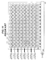
- FIG. 10 is a schematic plan view of a conventional solid state imaging device 800.
- the solid state imaging device 800 is the interlace-type CCD (ITCCD) most commonly used as a conventional solid state imaging device.
- a large number of photoelectric conversion elements (pixels) 812 are arranged in a tetragonal matrix in a light receiving region 802.
- a vertical electric charge transfer device (vertical charge coupled device: VCCD) 814 that reads out signal charges generated at the photoelectric conversion elements 812 and vertically transfers them is formed including transfer electrodes and a vertical transfer channel for each column of the photoelectric conversion elements 812 and transfers the signal charges generated at photoelectric conversion elements 12 in a vertical direction.
- a horizontal electric charge transfer device horizontal charge coupled device: HCCD 803 that transfers electric charges transferred by the VCCD 814 to a peripheral circuit 804 line by line is formed under the light receiving region 802.
- pixel lines on lines indicated with white arrows are first field lines in an interlace scanning method
- pixel lines on lines indicated with black arrows are second field lines.
- a color filter arrangement corresponding to each pixel is presented with letters "R, G and B" in each pixel.
- R, G and B respectively indicate red, green and blue.
- the color filter arrangement adopted in this solid state imaging device 800 is so-called Bayer arrangement and generally used for the solid state imaging device as an imaging device for a digital still camera (DSC).
- FIG. 11 is a schematic plan view of a conventional solid state imaging device 900.
- the solid state imaging device 900 is composed including a light receiving region 2 including vertical electric charge transfer devices (VCCD) 14 that vertically transfer signal charges generated at a large number of photoelectric conversion elements 12 and the photoelectric conversion elements, a horizontal electric charge transfer device (HCCD) that horizontally transfers the signal charges transferred by the VCCDs 14 and an output amplifier 4.
- VCCD vertical electric charge transfer devices
- HCCD horizontal electric charge transfer device
- the receiving light region 902 of the solid state imaging device to which Pixel Interleaved Array CCD (PIACCD) is adopted as shown in the drawing has a large number of pixels arranged in the pixel interleaved arrangement.
- a vertical electric charge transfer device 914 that reads out the signal charges generated at the photoelectric conversion elements 912, and vertically transfers them is provided with a vertically winding space between the columns of the photoelectric conversion elements 912.
- a transfer channel is positioned to the winding space formed by the pixel interleaved arrangement, and adjacent transfer channels are separated via the photoelectric conversion elements and come closer via the channel stop region 913 (for example, refer to JP-A Hei10-136391 (patent document 1) and Tetsuo Yamada and others, "A Progressive Scan CCD Imager for DSC Applications", ISSCC Digest of Technical Papers, February, 2002, Page 110 (non-patent document 1)).
- Each of the vertical electric charge transfer devices 914 is formed including a vertical transfer channel (not shown in the drawing) and transfer electrodes formed to a horizontal direction over the vertical transfer channel via an insulating film (not shown in the drawing) winding a space between horizontally adjacent photoelectric conversion elements 12.
- the color of the color filter (for example, green, blue or red) corresponding to each pixel is indicated by the letter G, B and R in each of the pixels 912.
- pixel lines on lines indicated with white arrows are first field lines in the interlace scanning method
- pixel lines on lines indicated with black arrows are second field lines.
- each G-line is formed along a solid line repeatedly connecting a center of each pixel.
- FIG. 12A to FIG. 12D are diagrams showing signal arrangements read by the conventional ITCCD solid state imaging device 800.
- FIG. 12A is a diagram showing a signal arrangement of the first field
- FIG. 12B is a diagram showing a signal arrangement of the second field.
- Both of the first field and the second field add same colored signals in every two lines.
- FIG. 12C a signal arrangement of a vertical two -pixel addition field synthesized frame generated by synthesizing each field after the vertical addition can be obtained.
- the conventional reading method for the ITCCD cannot reproduce a colored motion picture. Because each field includes only two types of signals such as G and R color signals or G and B color signals, one field cannot generate color signals including all of R, G, and B color signals. Since the color signal including R, G and B can be naturally generated after the field synthesis, the color signal after the synthesis, for example, can be used for a still picture with decreased number of pixels. In this case, sensitivity will be about doubled by the addition of the signals.
- FIG. 12D is a diagram showing spatial sampling centers after the vertical additions.
- the sampling points of G formed by the vertical addition of the first field with the Bayer Arrangement will be on lines indicated by white arrows, and the sampling points of G formed by the vertical addition of the second field with the Bayer Arrangement will be on lines indicated by black arrows.
- the sampling centers of the G signals after the vertical additions do not have regular intervals. Also, since the spatial sampling centers overlap with each another in wide areas, resolution obtained for the number of the sampling points will be lowered.
- FIG. 13A to FIG. 13D are diagrams showing signal arrangements read by the conventional PIACCD solid state imaging device 900.
- FIG. 13A is a diagram showing a signal arrangement of the first field
- FIG. 13B is a diagram showing a signal arrangement of the second field.
- the first field the first G-line and the third G-line are added, and the fifth G-line and the seventh G-line are added.
- the second field the second G-line and the fourth G-line are added, and the sixth G-line and the eighth G-line are added.
- FIG. 13C a signal arrangement of a vertical two-pixel addition field synthesized frame generated by synthesizing each field after the vertical addition can be obtained.
- each field includes color signal for all colors of RGB. Therefore, the color signals of RGB can be generated in one field, and colored motion picture signals can be generated.
- FIG. 13D is a diagram showing spatial sampling centers after the vertical additions.
- the sampling points of G obtained by the vertical addition of the first field with this conventional solid state imaging device 900 are on a line indicated by white arrow, and those by the vertical addition of the second field are on a line indicated by black arrow. That is, as in the case of the conventional solid state imaging device 800 shown in FIG. 12D, the sampling centers of the G signals after the vertical additions do not have regular intervals. Also, since spatial sampling ranges of the adjoining sampling points are overlapped with each other in a wide range, resolution obtained for the number of the sampling points will be lowered.
- a solid state imaging device comprising: a semiconductor substrate defining a two-dimensional surface; a plurality of photoelectric conversion elements disposed in a light receiving area of said semiconductor substrate in a plurality of rows and columns; an electric charge read-out device that reads out signal electric charges accumulated in said plurality of photoelectric conversion elements in interlace by dividing the signal electric charges in a plurality of fields, each field at least including the signal electric charges accumulated in the vertically adjacent photoelectric conversion elements corresponding to one color; and a vertical adding device that adds, for each field, the read-out signal electric charges divided into the plurality of fields.
- a solid state imaging device that can increase vertical resolution at a time of an interlace operation.
- FIG. 1 is a schematic plan view of a solid state imaging device 100 according to a first embodiment of the present invention.
- a solid state imaging device 100 at least includes a receiving region 2 having a large number of photoelectric conversion elements 12 and a vertical electric charge transfer device (vertical charge coupled device: VCCD) 14 that vertically transfers signal charge generated by the photoelectric conversion elements 12, a horizontal electric charge transfer device (horizontal charge coupled device: HCCD) 3 that horizontally transfers the signal charge transferred by the VCCD 14 and an output amplifier 4.
- VCCD vertical charge coupled device
- HCCD horizontal electric charge transfer device
- the light receiving region 2 of the solid-state imaging device 100 is consisted of the photoelectric conversion elements 12 disposed in a matrix with a so-called pixel interleaved arrangement (PIA) or a honeycomb arrangement.
- the pixel interleaved arrangement (PIA) represents an arrangement having a first lattice of a two-dimensional tetragonal matrix and a second lattice having each apex disposed on a center of apices of the first lattice.
- the photoelectric conversion elements 12 in the even number columns (lines) and in the odd number columns (lines) are shifted in the horizontal (vertical) direction by about a half of horizontal (vertical) pitch of the photoelectric conversion elements 12, and each column (line) of the photoelectric conversion elements 12 includes the photoelectric conversion elements 12 in only an even number line (column) or an odd number line (column).
- the expression "about a half" pitch is intended to include not only an exact half pitch but also a substantially equal to the exact half pitch that can be considered as a half pitch from the performance and image quality of a manufactured solid state imaging device although the pitch may be different from the exact half pitch. That is because the pitch of the photoelectric conversion elements may vary due to manufacture tolerances, rounding errors of pixel positions caused by a design or a mask formation, or the like.
- the above “a half pitch of photoelectric conversion elements 12 in the line of photoelectric conversion element” is the same.
- a vertical electric charge transfer device 14 that reads out and vertically transfers the signal charge generated at the photoelectric conversion elements 12 is winding through spaces between the adjoining photoelectric conversion elements 12.
- a winding transfer channel is configured in the spaces formed by the pixel interleaved arrangement, and adjoining transfer channels separate further via the photoelectric conversion elements 12 and approach closer to each other via the channel stop region 13 (FIG. 3).
- the vertical electric charge transfer device 14 consists of a vertical transfer channel (not shown in the drawing) and transfer electrodes (FIG. 3) formed above the vertical transfer channel via an insulating film (not shown in the drawing) and winds through the spaces between the photoelectric conversion elements 12 in a horizontal direction.
- a color filter is formed above each photoelectric conversion element 12.
- G, B and R respectively indicate the color filter of green, blue and red.
- pixel lines on lines indicated by white arrows are first field lines in an interlace scanning
- pixel lines on lines indicated by black arrows are second field lines.
- each G- line is formed along with a solid line repeatedly connecting centers of the pixels.
- each of the first G-lines and the fifth G-lines is formed in sharply alternating directions along with a solid line repeatedly connecting centers of a G-pixel in the first column, an R-pixel in the second column adjoining to a lower right of the G-pixel in the first column, a G-pixel in the third column adjoining to an upper right of the R-pixel in the second column and a B-pixel in the fourth column adjoining to a lower right of the G-pixel in the third column.
- each of the second G-lines and the sixth G-lines is formed in sharply alternating directions along with a solid line repeatedly connecting centers of a G-pixel in the first column, an R-pixel in the second column adjoining to a upper right of the G-pixel in the first column, a G-pixel in the third column adjoining to an lower right of the R-pixel in the second column and a B-pixel in the fourth column adjoining to a upper right of the G-pixel in the third column.
- each of the third G-lines and the seventh G-lines is formed in sharply alternating directions along with a solid line repeatedly connecting centers of a G-pixel in the first column, a B-pixel that is the closest to a lower right of the G-pixel in the first column, a G-pixel in the third column that is positioned on the same horizontal line as the G-pixel in the first column and an R-pixel in the fourth column that is the closest to a lower right of the G-pixel in the third column.
- each of the fourth G-lines and the eighth G-lines is formed in sharply alternating directions along with a solid line repeatedly connecting centers of a G-pixel in the first column, a B-pixel in the second column adjoining to a lower right of the G-pixel in the first column, a G-pixel in the third column adjoining to an upper right of the B-pixel in the second column and an R-pixel in the fourth column adjoining to a lower right of the G-pixel in the third column.
- FIG. 2A to FIG. 2D are diagrams showing signal arrangements read by the solid state imaging device 100 according to the first embodiment of the present invention.
- FIG. 2A is a diagram showing a signal arrangement of the first field
- FIG. 2B is a diagram showing a signal arrangement of the second field.
- G-lines adjoining each other in the vertical direction exist in each field.
- these adjoining G-lines are added vertically. That is, the first G-lines and the second G-lines, the fifth G-lines and the sixth G-lines are respectively added in the first field, and the third G-lines and the fourth G-lines, and the seventh G-lines and the eighth G-lines are respectively added in the second field.
- FIG. 2C a signal arrangement of a vertical two-pixel addition field synthesized frame generated by synthesizing each field after the vertical additions can be obtained.
- FIG. 2D is a diagram showing spatial sampling centers after the vertical additions.
- the G-lines the signals of the G-pixels
- FIG. 2D the centers of the sampling points of G in a vertical direction after the field synthesis will be on a line indicated by white arrows after the vertical addition for the first field and on lines indicated by black arrows after the vertical addition for the second field. Therefore, as shown in FIG. 2D, the centers of the sampling points are arranged with regular vertical intervals.
- FIG. 3 is a plan view showing an electrode structure of the solid state imaging device 100 according to the first embodiment of the present invention.
- the transfer electrodes 16 have a well-known double-layered structure, and each of them is consisted of a first layer electrode 16a and a second layer electrode 16b.
- the photoelectric conversion elements (pixels) 12 perform photoelectric conversion and accumulate electric charges, and colors of the color filter corresponding to the pixels are presented by putting letters "R", "G” and "B” in each pixel 12 in the drawing.
- phases of transferring pulses provided to electrodes are indicated with ⁇ V1 to ⁇ V8.
- an eight-phase driving method in which one transfer unit is consisted of eight electrodes (four electrodes for each pixel) is used in a normal interlace operation in the solid state imaging device with pixel interleaved arrangement.
- the signal charges accumulated in the pixels 12 are transferred to regions under the transfer electrodes on the read-out channel 18 side (a direction without the channel stop 19) as indicated by arrows. That is, when ⁇ V1 becomes high level, the signals of the B-pixels are transferred, and when ⁇ V3A, ⁇ V3B, ⁇ V7A and ⁇ V7B become high level, the signals of the G-pixels are transferred.
- a structural difference in the electrode structure between this embodiment and the prior art is that ⁇ V3 is imposed by using two electrically independent lines of ⁇ V3A and ⁇ V3B, and ⁇ V7 is imposed by using two electrically independent lines of ⁇ V7A and ⁇ V7B.
- an image signal for both motion picture and still picture can be easily generated with double sensitivity and half vertical resolution.
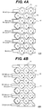
- FIG. 4A and FIG. 4B are plan views showing examples of an electrode structure of the solid state imaging device 200 according to a second embodiment of the present invention.
- the difference from the first embodiment is that a four-phase driving method in which one transfer unit consists of four electrodes (two electrodes for each pixel) is used in both of the structures shown in FIG. 4A and FIG. 4B.
- an image signal for both motion picture and still picture can be easily generated with double sensitivity and half vertical resolution.
- FIG. 5 is a schematic plan view of the solid state imaging device 300 according to a third embodiment of the present invention.
- Differences from the first embodiment and the second embodiment are points that a line memory 20 connected with the transfer channel of the vertical electric charge transfer device 14 is provided and a horizontal addition circuit 23 including an eight-phase driving horizontal transferring CCD (HCCD) is provided.
- HCCD horizontal transferring CCD
- Japanese Patent Application No. 2000-295896 Japanese Laid-Open Patent 2002-112119 filed by the same applicant as this invention gives details of the horizontal addition method by the horizontal addition circuit 23.
- signal charges in the first field are read out to the electric charge transfer devices 14, and the signal charges of two lines adjoining in the vertical direction are added in the electric charge transfer device 14 or in the line memory 20.
- the horizontal addition circuit 23 adds G-signals horizontally adjoining each other, adds the closest R-signals, and adds the closest B-signals.
- the signal charges in the second field are read out to the electric charge transfer device 14, and the signal charges of two lines adjoining to vertical direction are added in the electric charge transfer device 14 or the line memory 20.
- the horizontal addition circuit 23 adds G-signals horizontally adjoining each other, adds the closest R-signals, and adds the closest B-signals.
- each of the first field and the second field signals obtained by the signal additions shown in FIG. 6C and FIG. 6D is synthesized and defined as one frame signal.
- the signal additions are executed once in a vertical direction and once in a horizontal direction, that is the signal additions are executed twice as a whole. Therefore, the signal electric charge for one display pixel finally obtained will be four times that generated by one pixel.
- each of the vertical and horizontal resolutions will be decreased to a half of the original signals, and sensitivity will be increased to four times the original signals. Also, since the number of display pixels is decreased to 1/4, a frame rate can be increased to four times at the same data rate (a reading clock frequency).
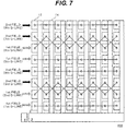
- FIG. 7 is a schematic plan view of a solid state imaging device 400 according to the fourth embodiment of the present invention.
- Structural differences between this fourth embodiment and the first embodiment are a point that the photoelectric conversion element 12 in the light receiving region 2 is arranged in a tetragonal matrix and a color filter arrangement.
- a large number of photoelectric conversion elements 12 are arranged in a tetragonal matrix in the light receiving region 2.
- a vertical electric charge transferring circuit (VCCD) 14 that reads the signal charges generated at the photoelectric conversion elements 12 and transfers them to a vertical direction is formed.
- the VCCD 14 includes the vertical transfer channel and transfer electrodes 16 and transfers the signal charges generated at the photoelectric conversion elements 12 to a vertical direction.
- a horizontal electric charge transferring circuit (HCCD) 3 that transfers every line of the signal charges transferred by the VCCD to a peripheral circuit 4 is formed.
- pixel lines on lines indicated with white arrows are first field lines in the interlace scanning, and pixel lines on lines indicated with black arrows are second field lines.
- each G-line is formed along with a straight line connecting centers of the pixels or a winding line repeatedly connecting centers of pixels.
- the first G-lines and the fifth G-lines consist of straight lines. That is, each of the first G-line and the fifth G-line is formed along with a solid line connecting the centers of G-pixel in the first column, the R-pixel in the second column adjoining the G-pixel in the first column, the G-pixel in the third column adjoining the R-pixel in the second column and the R-pixel in the fourth column adjoining the G-pixel in the third column (thereafter, this arrangement is repeated to the last column).
- each of the second G-line and the sixth G-line is formed by a line having sharply alternating directions along with a solid line repeatedly connecting centers of the G-pixel in the first column, the R-pixel in the second column adjoining to a upper right of the G-pixel in the first column, the G-pixel in the third column adjoining a lower right of the R-pixel in the second column and a B-pixel in the fourth column adjoining an upper right of the G-pixel in the third column.
- the fourth G-line and the eighth G-line consist of straight lines. That is, they are formed along with a solid line connecting the centers of the G-pixel in the first column, the B-pixel in the second column adjoining the G-pixel in the first column, the G-pixel in the third column adjoining the B-pixel and the B-pixel in the fourth column adjoining the G-pixel in the third column (hereinafter a repeat of this arrangement).
- each of the third G-line and the seventh G-line is formed by a line having sharply alternating directions along with a solid line repeatedly connecting centers of a G-pixel in the first column, an B-pixel in the second column adjoining a lower right of the G-pixel in the first column, a G-pixel in the third column adjoining an upper right of the B-pixel in the second column and a B-pixel in the fourth column adjoining a lower right of the G-pixel in the third column.
- FIG. 8A to FIG. 8D are diagrams showing signal arrangements read by the solid state imaging device 400 according to the fourth embodiment of the present invention.
- FIG. 8A is a diagram showing a signal arrangement of the first field
- FIG. 8B is a diagram showing a signal arrangement of the second field.
- G-lines adjoining each other to vertical direction exist in each field.
- these adjoining G-lines are added vertically. That is, the first G-lines and the second G-lines, the fifth G-lines and the sixth G-lines are respectively added in the first field, and the third G-lines and the fourth G-lines, and the seventh G-lines and the eighth G-lines are respectively added in the second field.
- FIG. 8C a signal arrangement of a vertical two-pixel addition field synthesized frame generated by synthesizing each field after the vertical additions can be obtained.
- FIG. 8D is a diagram showing spatial sampling centers after the vertical additions.
- the G-lines the signals of the G-pixels
- FIG. 8D the centers of the sampling points are arranged with regular vertical intervals.
- FIG. 9A and FIG. 9B are graphs for comparing a spatial resolution of either one of the first to fourth embodiments of the present invention with a spatial resolution of the prior art.
- FIG. 9A shows a spatial sampling response obtained by the conventional vertical additions
- FIG. 9B shows a spatial sampling response obtained by vertical additions according to any of the first to fourth embodiments of the present invention.
- solid lines indicate the spatial sampling responses in a first field
- dotted lines indicate the spatial sampling responses in a second field.
- the spatial resolution will be about twice that of the conventional vertical additions.
- sensitivity can be raised in proportion to the number of addition times.
- frame rate can be raised corresponding to the number of the addition times.
- the signals are read out in two steps such as the first field and the second field, it is not limited to that.
- the signals can be read out in three steps such as the first to the third steps, and one frame signal can be generated by synthesizing the signals in the first to the third fields.
- the first G-lines, the second G-lines, the seventh G-lines and the eighth G-lines are read out as the signals in the first field
- the third G-lines, the fourth G-lines, the ninth G-lines and the tenth G-lines are read out as the signals in the second field
- the fifth G-lines, the sixth G-lines, the eleventh G-lines and the twelfth G-lines are read out as the signals in the third field.
- the signal electric charges of the vertically adjoining G-pixel are added in the above-described first to fourth embodiments on the assumption that the G (green)-pixels define the resolution; however, the signal charges of the vertically adjoining pixels in other colors may be added.
- the other colors are not only R (red) and B (blue), but also, for example, white, etc.
- the embodiments has been explained by using the CCD-type solid state imaging device as examples, it is not limited to the CCD-type solid state imaging device.
- a CMOS-type solid state imaging device can be adapted for the present invention.
Landscapes
- Engineering & Computer Science (AREA)
- Multimedia (AREA)
- Signal Processing (AREA)
- Physics & Mathematics (AREA)
- General Physics & Mathematics (AREA)
- Solid State Image Pick-Up Elements (AREA)
- Transforming Light Signals Into Electric Signals (AREA)
Abstract
Description
Claims (8)
- A solid state imaging device (100) comprising:a semiconductor substrate defining a two-dimensional surface;a plurality of photoelectric conversion elements (12) disposed in a light receiving area (2) of said semiconductor substrate in a plurality of rows and columns;an electric charge read-out device (14) that reads out signal electric charges accumulated in said plurality of photoelectric conversion elements in interlace by dividing the signal electric charges into a plurality of fields, each field including at least the signal electric charges accumulated in the vertically adjacent photoelectric conversion elements corresponding to one color; anda vertical adding device (14) that adds, for each field, the read-out signal electric charges divided into the plurality of fields.
- The solid state imaging device according to claim 1, wherein said plurality of fields comprise a first field including signal electric charges read out from half the number of said plurality of photoelectric conversion elements and a second field including signal electric charges read out from remaining number of said plurality of photoelectric conversion elements.
- The solid state imaging device according to claim 1 or 2, wherein said one color is green (G).
- The solid state imaging device according to any preceding claim, wherein said vertical adding device vertically adds same color signals of each field including at least the signal electric charges accumulated in the vertically adjacent photoelectric conversion elements corresponding to one color.
- The solid state imaging device according to any preceding claim, wherein said plurality of photoelectric conversion elements are arranged in each of grids of a first tetragonal matrix and grids of a second tetragonal matrix that has grids on a center of the grids of the first tetragonal matrix.
- The solid state imaging device according to claim 5, wherein green (G) pixels are arranged on the grids of the first tetragonal matrix, and red (R) pixels and blue (B) pixels are alternatively arranged on the grids of the second tetragonal matrix.
- The solid state imaging device according to any preceding claim, further comprising a horizontal adding device (3) that horizontally adds signal electric charges in a same color vertically added for each field.
- The solid state imaging device according to any preceding claim, further comprising a frame generator that generates an image for one frame by synthesizing the signal electric charges of said plurality of fields in time and space.
Applications Claiming Priority (2)
| Application Number | Priority Date | Filing Date | Title |
|---|---|---|---|
| JP2004038266 | 2004-02-16 | ||
| JP2004038266A JP4183635B2 (en) | 2004-02-16 | 2004-02-16 | Solid-state imaging device |
Publications (2)
| Publication Number | Publication Date |
|---|---|
| EP1564813A2 true EP1564813A2 (en) | 2005-08-17 |
| EP1564813A3 EP1564813A3 (en) | 2007-10-10 |
Family
ID=34697955
Family Applications (1)
| Application Number | Title | Priority Date | Filing Date |
|---|---|---|---|
| EP05003091A Withdrawn EP1564813A3 (en) | 2004-02-16 | 2005-02-14 | Solid state imaging device with increased vertical resolution in interlace scanning method |
Country Status (4)
| Country | Link |
|---|---|
| US (1) | US7612812B2 (en) |
| EP (1) | EP1564813A3 (en) |
| JP (1) | JP4183635B2 (en) |
| KR (1) | KR100711120B1 (en) |
Families Citing this family (10)
| Publication number | Priority date | Publication date | Assignee | Title |
|---|---|---|---|---|
| CN1219395C (en) * | 2002-01-30 | 2005-09-14 | 株式会社理光 | Camera apparatus and camera method |
| JP4468052B2 (en) * | 2004-04-08 | 2010-05-26 | キヤノン株式会社 | IMAGING DEVICE AND IMAGING DEVICE CONTROL METHOD |
| US7221225B2 (en) | 2004-12-03 | 2007-05-22 | Micro-Mobio | Dual band power amplifier module for wireless communication devices |
| JP4603455B2 (en) * | 2005-10-06 | 2010-12-22 | 日本放送協会 | Solid-state imaging device |
| JP5038188B2 (en) * | 2008-02-28 | 2012-10-03 | キヤノン株式会社 | Imaging apparatus and imaging system using the same |
| JP5640509B2 (en) * | 2010-07-09 | 2014-12-17 | ソニー株式会社 | Solid-state imaging device and camera system |
| JP2012175600A (en) | 2011-02-24 | 2012-09-10 | Sony Corp | Imaging apparatus, imaging apparatus control method, and program |
| JP5621054B2 (en) * | 2011-12-27 | 2014-11-05 | 富士フイルム株式会社 | Color image sensor |
| JP6031835B2 (en) * | 2012-06-06 | 2016-11-24 | 株式会社ニコン | Imaging device |
| KR102242563B1 (en) | 2015-03-11 | 2021-04-20 | 삼성전자주식회사 | Pixel pattern and image sensor comprising the same |
Family Cites Families (27)
| Publication number | Priority date | Publication date | Assignee | Title |
|---|---|---|---|---|
| JPS57203387A (en) * | 1981-06-10 | 1982-12-13 | Toshiba Corp | Color television image pickup device |
| JPS57203389A (en) * | 1981-06-10 | 1982-12-13 | Toshiba Corp | Solid-state color image pickup device |
| JPS62210414A (en) * | 1986-03-12 | 1987-09-16 | Minolta Camera Co Ltd | Focus detecting device |
| US5457494A (en) * | 1988-11-21 | 1995-10-10 | Canon Kabushiki Kaisha | Image pickup signal processing apparatus |
| JPH05300437A (en) * | 1992-04-21 | 1993-11-12 | Mitsubishi Electric Corp | Solid-state image sensor |
| JP2978018B2 (en) * | 1992-11-10 | 1999-11-15 | 富士フイルムマイクロデバイス株式会社 | Solid-state imaging device and driving method thereof |
| JP3492029B2 (en) * | 1995-06-30 | 2004-02-03 | キヤノン株式会社 | Imaging device |
| JP3551571B2 (en) * | 1995-08-11 | 2004-08-11 | ソニー株式会社 | Color CCD solid-state imaging device |
| JP3830590B2 (en) * | 1996-10-30 | 2006-10-04 | 株式会社東芝 | Solid-state imaging device |
| JPH10136244A (en) * | 1996-11-01 | 1998-05-22 | Olympus Optical Co Ltd | Electronic image pickup device |
| JP4140077B2 (en) * | 1998-02-18 | 2008-08-27 | ソニー株式会社 | Solid-state image sensor driving method, solid-state image sensor, and camera |
| EP1017230B1 (en) * | 1998-12-28 | 2010-02-10 | SANYO ELECTRIC Co., Ltd. | Imaging apparatus and digital camera |
| JP3943273B2 (en) * | 1999-01-28 | 2007-07-11 | 富士フイルム株式会社 | Solid-state imaging device and signal readout method |
| JP2000308076A (en) | 1999-04-26 | 2000-11-02 | Hitachi Ltd | Imaging device |
| US7038723B1 (en) * | 1999-04-26 | 2006-05-02 | Matsushita Electric Industrial Co., Ltd. | Solid state imaging device, method for driving the same and camera using the same |
| US6992714B1 (en) * | 1999-05-31 | 2006-01-31 | Canon Kabushiki Kaisha | Image pickup apparatus having plural pixels arranged two-dimensionally, and selective addition of different pixel color signals to control spatial color arrangement |
| JP2001111894A (en) * | 1999-10-07 | 2001-04-20 | Fuji Film Microdevices Co Ltd | Solid-state imaging device, control method thereof, and solid-state imaging device using the same |
| JP3636291B2 (en) * | 2000-01-31 | 2005-04-06 | オリンパス株式会社 | Imaging device |
| US6876388B1 (en) * | 2000-02-02 | 2005-04-05 | Taiwan Advanced Sensors Corporation | Interlaced alternating pixel design for high sensitivity CMOS Image sensors |
| JP4497261B2 (en) * | 2000-09-28 | 2010-07-07 | 富士フイルム株式会社 | Charge transfer device, CCD image sensor, and CCD imaging system |
| JP2003060185A (en) * | 2001-08-21 | 2003-02-28 | Fuji Film Microdevices Co Ltd | Solid-state image pickup device and control method therefor |
| US7202900B2 (en) * | 2001-08-22 | 2007-04-10 | Florida Atlantic University | Method of producing frame pair signals from an image sensor and method for displaying same |
| JP3877565B2 (en) * | 2001-10-04 | 2007-02-07 | 松下電器産業株式会社 | Imaging device |
| JP2003163937A (en) * | 2001-11-26 | 2003-06-06 | Fuji Photo Film Co Ltd | Solid-state imaging device and imaging apparatus |
| JP2003299112A (en) * | 2002-03-29 | 2003-10-17 | Fuji Photo Film Co Ltd | Digital camera |
| JP3925479B2 (en) | 2003-09-16 | 2007-06-06 | 株式会社日立製作所 | Imaging device |
| JP5033711B2 (en) * | 2007-06-13 | 2012-09-26 | 富士フイルム株式会社 | Imaging device and driving method of imaging device |
-
2004
- 2004-02-16 JP JP2004038266A patent/JP4183635B2/en not_active Expired - Fee Related
-
2005
- 2005-02-14 EP EP05003091A patent/EP1564813A3/en not_active Withdrawn
- 2005-02-15 US US11/057,751 patent/US7612812B2/en not_active Expired - Fee Related
- 2005-02-16 KR KR1020050012879A patent/KR100711120B1/en not_active Expired - Fee Related
Also Published As
| Publication number | Publication date |
|---|---|
| US20050179798A1 (en) | 2005-08-18 |
| JP4183635B2 (en) | 2008-11-19 |
| KR100711120B1 (en) | 2007-04-24 |
| JP2005229503A (en) | 2005-08-25 |
| US7612812B2 (en) | 2009-11-03 |
| KR20060042014A (en) | 2006-05-12 |
| EP1564813A3 (en) | 2007-10-10 |
Similar Documents
| Publication | Publication Date | Title |
|---|---|---|
| US6236434B1 (en) | Solid state image pickup device | |
| US7440019B2 (en) | Solid-state image pick-up device | |
| JP4497688B2 (en) | Solid-state imaging device | |
| US7218348B2 (en) | Solid-state electronic imaging device and method of controlling opertion thereof | |
| US6885399B1 (en) | Solid state imaging device configured to add separated signal charges | |
| US7612812B2 (en) | Solid state imaging device with increased vertical resolution in interlace scanning method | |
| US6822682B1 (en) | Solid state image pickup device and its read method | |
| JP4207736B2 (en) | Solid-state imaging device | |
| JP4252685B2 (en) | Solid-state imaging device | |
| US7655892B2 (en) | Solid-state imaging device, and method of driving solid-state imaging device | |
| JP4354346B2 (en) | Solid-state imaging device, driving method thereof, and camera equipped with the same | |
| JP4514912B2 (en) | Solid-state imaging device and driving method thereof | |
| US7465910B2 (en) | Solid state imaging device with increased vertical and horizontal resolutions in interlace scanning method | |
| JP2006014075A5 (en) | ||
| JP4132003B2 (en) | Solid-state imaging device | |
| JP3277974B2 (en) | Solid-state imaging device | |
| EP1708483B1 (en) | Solid state imaging apparatus and driving method of the solid state imaging apparatus | |
| JP3704406B2 (en) | Solid-state imaging device | |
| JP2004214363A (en) | Solid imaging device and digital camera | |
| EP0133835A2 (en) | CCD area image sensor and method for color imaging | |
| US20060164532A1 (en) | Solid state imaging apparatus and driving method for the solid stateimaging apparatus | |
| JP2003060185A (en) | Solid-state image pickup device and control method therefor | |
| JP3021513B2 (en) | Solid-state imaging device | |
| JP2001057419A (en) | Solid-state image sensor and its manufacture | |
| US20060028570A1 (en) | Solid state image capturing device and control method thereof |
Legal Events
| Date | Code | Title | Description |
|---|---|---|---|
| PUAI | Public reference made under article 153(3) epc to a published international application that has entered the european phase |
Free format text: ORIGINAL CODE: 0009012 |
|
| AK | Designated contracting states |
Kind code of ref document: A2 Designated state(s): AT BE BG CH CY CZ DE DK EE ES FI FR GB GR HU IE IS IT LI LT LU MC NL PL PT RO SE SI SK TR |
|
| AX | Request for extension of the european patent |
Extension state: AL BA HR LV MK YU |
|
| RAP1 | Party data changed (applicant data changed or rights of an application transferred) |
Owner name: FUJIFILM CORPORATION |
|
| PUAL | Search report despatched |
Free format text: ORIGINAL CODE: 0009013 |
|
| AK | Designated contracting states |
Kind code of ref document: A3 Designated state(s): AT BE BG CH CY CZ DE DK EE ES FI FR GB GR HU IE IS IT LI LT LU MC NL PL PT RO SE SI SK TR |
|
| AX | Request for extension of the european patent |
Extension state: AL BA HR LV MK YU |
|
| 17P | Request for examination filed |
Effective date: 20071113 |
|
| 17Q | First examination report despatched |
Effective date: 20080313 |
|
| AKX | Designation fees paid |
Designated state(s): DE FR GB |
|
| STAA | Information on the status of an ep patent application or granted ep patent |
Free format text: STATUS: THE APPLICATION IS DEEMED TO BE WITHDRAWN |
|
| 18D | Application deemed to be withdrawn |
Effective date: 20120211 |