EP1564645A2 - Konfigurierbares Speichersystem für einen embedded Prozessor - Google Patents
Konfigurierbares Speichersystem für einen embedded Prozessor Download PDFInfo
- Publication number
- EP1564645A2 EP1564645A2 EP05002812A EP05002812A EP1564645A2 EP 1564645 A2 EP1564645 A2 EP 1564645A2 EP 05002812 A EP05002812 A EP 05002812A EP 05002812 A EP05002812 A EP 05002812A EP 1564645 A2 EP1564645 A2 EP 1564645A2
- Authority
- EP
- European Patent Office
- Prior art keywords
- memory
- memory component
- processing core
- component
- embedded processor
- Prior art date
- Legal status (The legal status is an assumption and is not a legal conclusion. Google has not performed a legal analysis and makes no representation as to the accuracy of the status listed.)
- Ceased
Links
Images


Classifications
-
- G—PHYSICS
- G06—COMPUTING OR CALCULATING; COUNTING
- G06F—ELECTRIC DIGITAL DATA PROCESSING
- G06F15/00—Digital computers in general; Data processing equipment in general
- G06F15/76—Architectures of general purpose stored program computers
- G06F15/78—Architectures of general purpose stored program computers comprising a single central processing unit
- G06F15/7839—Architectures of general purpose stored program computers comprising a single central processing unit with memory
- G06F15/7842—Architectures of general purpose stored program computers comprising a single central processing unit with memory on one IC chip (single chip microcontrollers)
- G06F15/7846—On-chip cache and off-chip main memory
-
- G—PHYSICS
- G06—COMPUTING OR CALCULATING; COUNTING
- G06F—ELECTRIC DIGITAL DATA PROCESSING
- G06F30/00—Computer-aided design [CAD]
- G06F30/30—Circuit design
Definitions
- the present invention relates to microprocessors, and more particularly to a floor plan friendly configurable memory system.
- microprocessors Modern electronic systems are increasingly using microprocessors to provide greater flexibility and functionality. For example, many home entertainment components such as DVD players include microprocessors to perform video decompression. Computer peripherals such as laser printers, modems, and disk drives also include microprocessors to perform various functions. In the past many of these devices used microprocessors on circuit boards. The circuit boards would include support chips for the microprocessor such as memory, as well as chips to perform the functions of the overall device.
- microprocessors which are "embedded” within the system, are generally referred to as embedded processors.
- embedded processor includes a processing core, the memory system for the processing core, and support logic for the processing core and memory system.
- processors including microprocessors, microcontrollers, and embedded processors are so difficult, most users purchase the microprocessors from a handful of processor companies that have expertise in designing, simulating, laying out, producing and verifying processors.
- Fig. 1(a) illustrates an embedded processor 110 having a regular rectangular shape.
- Fig. 1 (b) illustrates an embedded processor 120 having a irregular shape.
- embedded processor 120 has rectangular shape that is missing a notch 125.
- Embedded processor system 110 and embedded processor 120 require the same silicon area.
- notch 125 might not be useable by other components of the system due to layout, placement, or routing issues. Therefore, effectively, embedded processor 120 would require more silicon area than embedded processor 110 due to the irregular shape of embedded processor 120. Therefore, embedded processor 110 would be more expensive to use than embedded processor 110.
- embedded processors must support multiple memory configurations to satisfy different customers.
- changing the size of different memory components or selecting different memory components often lead to irregular shaped embedded processors.
- notch 125 may be caused in embedded processor 120 because embedded processor 120 is configured to not include a program cache.
- Notches or other irregularities can also be caused by using differently sized memory banks or memory towers.
- the layout of some embedded processors are redone to avoid the notches or other irregularities, however redoing a layout is extremely time consuming and may would entail risk of error in the layout process.
- a configurable memory system for embedded processors in accordance with one embodiment of the present invention is arranged to have a regular rectangular shape in all configurations of the memory system.
- the silicon area required by an embedded processor using the configurable memory system does not include notches or other irregular features that may cause wasted silicon area.
- customers can design a semi-custom embedded processor by selecting memory components and configuring the memory components with respect to the memory sizes, the number of ways (for cache memories), the type of memories and various other features.
- the memory components are generated so that the total width of a memory component is the same as other memory components as well as the same width as the processing core.
- a program cache with four memory towers.
- the total width of the memory component is equal to the sum of the widths of the four memory towers.
- the total width of the four memory towers would be equal to the width of the processing core.
- the embedded processor is laid out so that a first memory component is adjacent to a first side of the processing core and a second memory component is adjacent to the first memory component and on opposite sides of the first memory component with respect to the processing core.
- a third memory component can be placed adjacent to the processing core on an opposite side of the processing core with respect to the first memory component.
- memory components form a first stack on one side of the processing core and can form a second stack on the opposite side of the processing core.
- Each stack can contain several memory components. Even though the memory components can be of different types and different memory sizes, the width of the memory components and the processing core are kept the same so that the embedded processor has a rectangular shape.
- Fig. 1(a) illustrates the shape of an embedded memory system.
- Fig. 1(b) illustrates the shape of an embedded memory system having an irregular feature that may cause wasted silicon area.
- Fig. 2 is a simplified block diagram of an embedded processor with a memory system in accordance with one embodiment of the present invention.
- Fig. 3 is a simplified block diagram of an embedded processor with a memory system in accordance with one embodiment of the present invention.
- Fig. 4 is a process flow diagram in accordance with one embodiment of the present invention.
- Fig. 5 is a block diagram of a cache in accordance with one embodiment of the present invention.
- Fig. 6 is a block diagram of a scratch pad memory in accordance with one embodiment of the present invention.
- Embedded processors with configurable memory systems can be customized for customers having different requirements.
- different memory configurations, especially memory configuration involving different memory systems and types of memory lead to irregular features in the shape of the embedded processor
- the area of the irregular shapes are generally not useable by other logic circuits on the die and thus would result in wasted area on the die, which may lead to higher costs.
- the present invention uses a novel memory architecture to minimize the occurrence of irregular features on the shape of the embedded processor irregardless of the memory configuration selected.
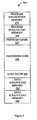
- Fig. 2 is a simplified block diagram of an embedded processor architecture 200 in accordance with one embodiment of the present invention.
- Embedded processor architecture 200 includes a processing core 210 with a configurable memory system having a data cache 220, a first data scratch pad memory 230, and a second data scratch pad memory 240, a program cache 250, a program scratch pad memory 260, and a program scratch pad memory 270.
- processing Core 210 includes the main processing elements such as the arithmetic logic unit (ALU), the integer pipeline, load/store pipeline and memory interfaces.
- ALU arithmetic logic unit
- Some embodiments of the present invention also include clock trees in processing core 210.
- Data cache 230 is located adjacent to processing core 210 to minimize propagation delays between processing core 210 and data cache 230.
- Data scratch pad memory 230 is located adjacent to the side of data cache 220 that is opposite the side adjacent to processing core 210.
- Data scratch pad memory 240 is located adjacent to the side of data scratch pad memory 230 that is opposite the side adjacent to data cache 220.
- Program cache 250 is located adjacent to processing core 210 to minimize propagation delays between processing core 210 and program cache 250. Specifically, Data cache 230 and program cache 250 are located on opposite sides of processing core 210 to minimize irregular features in the various memory configurations as described below.
- Program scratch pad memory 260 is located adjacent to the side of program cache 250 that is opposite the side adjacent to processing core 210.
- Program scratch pad memory 270 is located adjacent to the side of program scratch pad memory 260 that is opposite the side adjacent to program cache 250.
- different memory components have differing priority levels, the higher the priority level the closer the memory component should be to the processing core. Thus, caches would in general have higher priority levels than scratch pad memory, because the physical timing of caches is more critical than scratch pad memories.
- each memory component is equal and does not change with the size of each memory component.
- width as used herein with respect to the memory components and the processing core refers to the dimension parallel to the sides of processing core 210 that are adjacent to the memory components.
- length refers to the dimension perpendicular to the side of processing core 210 that is adjacent to the memory components.
- the width of the memory components should be no larger than the width of processing core 210.
- Most embodiments of the present invention attempt to make the width of the memory components and the width of processing core 210 equal so that embedded processor 200 has a rectangular shape.
- width of the processing core and the width of all the memory components are designed to be equal, regardless of the size or type of the memory component.
- the minimum width of a memory component is dependent on the number of sense amps that are activated in one memory access. Generally, caches that are fully associative or set associative would require more sense amps than the scratch pad memories.
- most embodiments of the present invention make use of additional post sense amp multiplexers as necessary to make the widths of the different memory components equal.
- the memory system is configurable to include or to not include the various caches and scratch pad memories. Furthermore each cache and scratch pad memory can be configured to a variety of different sizes. The placement of the memory components depend on the priority level of the memory component. As explained above, caches generally have higher priority levels than scratch pad memories. If a high priority level memory component, such as a cache is omitted, lower priority memory components that were further from processing core 210 would move closer to processing core 210 to replace the omitted memory component. For example, if data cache 220 is omitted in a particular memory configuration, data scratch pad memory 230 slide up to be placed adjacent to processing core 210, and data scratch pad memory 240 would slide up to remain adjacent to data scratch pad memory 230. Because the memory components have the same width, omission or inclusion of each memory component does not introduce irregular features to the shape of the embedded processor.
- a memory generator generates a particular memory component to match the specification of the memory component during the creation of the design file for the embedded processor. In other embodiments, most of the different configurations of the memory components are pre-generated.
- Fig. 3 illustrates a different configuration of an embedded processor.
- the embedded processor omits the program cache and one of the program scratch pad memories.
- the embedded processor of Fig. 3 has a processing core 210-a, a large program scratch pad memory 260-a, a data cache 220-a, a first data scratch pad memory 230-a and a second data scratch pad memory 240-a.
- the memory components further from the processing core slide closer to the processing core.
- the omission of the program cache allows program scratch pad memory 260-a to be adjacent to processing core 210-a.
- Program scratch pad memory 260-a has a larger memory size than program scratch pad memory 260 (Fig. 2).
- program scratch pad memory 260-a has a greater length than program scratch pad memory 260.
- the embedded processor of Fig. 3 retains a rectangular shape without irregular features that may waste silicon area.
- a primary benefit of the present invention is that regardless of the changes in the memory configuration, the process core can remain unchanged.
- Fig. 4 illustrates a process flow 400 in the creation of a specific configuration of a configurable embedded processor for a customer.
- the design and layout of the processing core has already been completed.
- step memory component selection stage 410 the customer selects which memory components are present in the embedded processor.
- step memory component configuration stage 420 the customer decides on the memory size, memory type, and features of the memory components.
- a memory generator For example if the memory component is a cache, the customer may be able to select different size sets and different number of "ways" in a N-Way set associative cache. Then, in memory generation stage 430, a memory generator generates the memory components that have the same width as the processing core and that match the customer's configuration. Because memory components have the same width, memory components having larger memory size would have a greater length than memory components having a smaller memory size. As used herein, generating a memory component includes referencing a pre-generated memory component design that could be for example stored in a memory component library. Then, in processor layout generation stage 440, the memory components are attached to the processing core based on priority. In most embodiments of the present invention, priority is based on critical timing within one memory cycle.
- the physical timing of a cache is in general more critical than the physical timing of a scratch pad memories, thus caches have higher priority than scratch pad memories.
- the program memory components are placed adjacent to one side of the processing core and the data memory components are placed adjacent an opposite side of the processing core. Because the memory components are the same width as the processing core, the embedded processor has a rectangular shape.
- Fig. 5 illustrates a cache 500 in accordance with one embodiment of the present invention.
- Cache 500 which can be used as a program cache or a data cache, includes four cache towers 510, 520, 530 and 540, a tag unit 550, and a multiplexing circuit 560.
- Tag unit 550 and cache towers 510, 520, 530, and 540 receive an address ADDR.
- Tag unit 550 determines whether cache 500 is caching address ADDR. And generates a hit signal HIT to indicate whether address ADDR is cached in cache 500.
- each cache tower provides one half word (16 bits of data) during each memory access.
- Cache 500 is 4-way set associative thus each cache tower is logically subdivided (not shown) into 4 way sub-towers that are each logically 16 bits wide. All four way sub-towers are activated simultaneously to select the proper 16 bits of data.
- each cache tower has at least 64 sense amps.
- each cache tower in cache 500 may physically include more sense amps which are multiplexed down to the logical 64 bits.
- Each cache tower is physically identical and has a fixed width to accommodate the sense amps. While the cache towers in a specific instance of cache 500 are identical, different instances of cache 500, which are of different size, will have cache towers of different lengths.
- Multiplexing circuit 560 receives data from all the "ways" and provides the data from the appropriate "way” as data DATA.
- multiplexing circuit 560 may act as a data aligner, which rearranges the order of the data as needed to support unaligned access. Operation of a Cache that supports unaligned access is described in co-owned and co-pending U.S. Patent Application No. [Attorney Docket No. INF-023], entitled “Fast Unaligned Cache Access System and Method" by Oberlaender, which is herein incorporated by reference.
- Fig. 6 illustrates a scratch pad memory 600 in accordance with one embodiment of the present invention.
- Scratch pad memory 600 which can be used as program scratch pad memory or data scratch pad memory, includes four memory towers 610, 620, 630, and 640.
- each memory tower logically provides a half word (16 bits) during a memory access.
- Four memory towers are used in scratch pad memory to support unaligned memory accesses as described in co-owned and co-pending U.S. Patent Application [Attorney Docket No. INF-025], by Oberlaender, et al., entitled "Fast Unaligned Memory Access System and Method, which is herein incorporated by reference.
- each memory tower only requires 16 sense amps.
- the memory components and the processing core are configured to have the same width.
- the present memory towers are generated to use more bit lines and sense amps to make use of the additional width of the memory component.
- Multiplexing within each memory towers reduces the physical number of data bits from the sense amps to the logical number of bits required.
- caches are 4 way set associative and each cache tower require with 64 logical bits of output.
- the cache towers are implemented with 256 sense amps and 4 to 1 multiplexing to reduce the 256 bits from the sense amps to the 64 logical bits.
- the memory towers are also implemented using 256 sense amps.
- the memory towers require 16 logical bits of data. Therefore, each memory tower uses 16 to 1 multiplexing to reduce the 256 bits of data from the sense amps to the required 16 bits.
- novel structures and methods have been described to provide a configurable memory system for an embedded processor that allows the embedded processor to have a rectangular shape despite changing memory configurations. Keeping a rectangular shape reduces the likelihood of wasted silicon area on a system using the embedded processor, which leads to lower costs in producing the system, greater flexibility, and faster time to market. Furthermore, the present invention reduces risk of errors because the processing core does not need to change between various configurations of the embedded processor.
- the various embodiments of the structures and methods of this invention that are described above are illustrative only of the principles of this invention and are not intended to limit the scope of the invention to the particular embodiments described.
Landscapes
- Engineering & Computer Science (AREA)
- Computer Hardware Design (AREA)
- Theoretical Computer Science (AREA)
- Physics & Mathematics (AREA)
- General Engineering & Computer Science (AREA)
- General Physics & Mathematics (AREA)
- Evolutionary Computation (AREA)
- Geometry (AREA)
- Memory System Of A Hierarchy Structure (AREA)
- Logic Circuits (AREA)
- Advance Control (AREA)
Applications Claiming Priority (2)
| Application Number | Priority Date | Filing Date | Title |
|---|---|---|---|
| US777863 | 1996-12-31 | ||
| US10/777,863 US7281228B2 (en) | 2004-02-11 | 2004-02-11 | Configurable memory system for embedded processors |
Publications (2)
| Publication Number | Publication Date |
|---|---|
| EP1564645A2 true EP1564645A2 (de) | 2005-08-17 |
| EP1564645A3 EP1564645A3 (de) | 2006-09-27 |
Family
ID=34701386
Family Applications (1)
| Application Number | Title | Priority Date | Filing Date |
|---|---|---|---|
| EP05002812A Ceased EP1564645A3 (de) | 2004-02-11 | 2005-02-10 | Konfigurierbares Speichersystem für einen embedded Prozessor |
Country Status (2)
| Country | Link |
|---|---|
| US (1) | US7281228B2 (de) |
| EP (1) | EP1564645A3 (de) |
Cited By (1)
| Publication number | Priority date | Publication date | Assignee | Title |
|---|---|---|---|---|
| KR20230074955A (ko) * | 2021-11-22 | 2023-05-31 | 리벨리온 주식회사 | 재구성가능 온 칩 메모리 뱅크, 재구성가능 온 칩 메모리, 이를 탑재한 시스템 온 칩 및 재구성가능 온 칩 메모리 사용 방법 |
Families Citing this family (2)
| Publication number | Priority date | Publication date | Assignee | Title |
|---|---|---|---|---|
| EP1975791A3 (de) * | 2007-03-26 | 2009-01-07 | Interuniversitair Microelektronica Centrum (IMEC) | Verfahren für automatisierte Codeumwandlung |
| CN102915293B (zh) * | 2012-08-30 | 2015-07-22 | 杭州晟元芯片技术有限公司 | 一种soc内的系统架构内的硬件资源的复用方法 |
Family Cites Families (10)
| Publication number | Priority date | Publication date | Assignee | Title |
|---|---|---|---|---|
| JPS6381569A (ja) | 1986-09-26 | 1988-04-12 | Hitachi Ltd | マイクロコンピユ−タの設計方式 |
| KR940004434A (ko) | 1992-08-25 | 1994-03-15 | 윌리엄 이. 힐러 | 스마트 다이나믹 랜덤 억세스 메모리 및 그 처리방법 |
| JPH09231130A (ja) * | 1996-02-26 | 1997-09-05 | Mitsubishi Electric Corp | マイクロコンピュータ |
| US5812418A (en) | 1996-10-31 | 1998-09-22 | International Business Machines Corporation | Cache sub-array method and apparatus for use in microprocessor integrated circuits |
| JPH1115773A (ja) | 1997-06-24 | 1999-01-22 | Matsushita Electron Corp | 半導体集積回路、コンピュータシステム、データ処理装置及びデータ処理方法 |
| US6553552B1 (en) | 2000-01-27 | 2003-04-22 | National Semiconductor Corporation | Method of designing an integrated circuit memory architecture |
| US6412038B1 (en) | 2000-02-14 | 2002-06-25 | Intel Corporation | Integral modular cache for a processor |
| US6493855B1 (en) | 2000-02-18 | 2002-12-10 | Hewlett-Packard Company | Flexible cache architecture using modular arrays |
| US6633960B1 (en) * | 2000-08-31 | 2003-10-14 | Hewlett-Packard Development Company, L.P. | Scalable directory based cache coherence protocol |
| US20050108711A1 (en) * | 2003-11-13 | 2005-05-19 | Infineon Technologies North America Corporation | Machine instruction for enhanced control of multiple virtual processor systems |
-
2004
- 2004-02-11 US US10/777,863 patent/US7281228B2/en not_active Expired - Lifetime
-
2005
- 2005-02-10 EP EP05002812A patent/EP1564645A3/de not_active Ceased
Non-Patent Citations (1)
| Title |
|---|
| GUY RABBAT: "Hardware and Software Concepts in VLSI - Chapter 16", 1983, VAN NOSTRAND REINHOLD COMPANY, New York, ISBN: 0-442-22538-5, article R M J M OTTEN: "VLSI Layout", pages: 406 - 451, XP002559472 * |
Cited By (1)
| Publication number | Priority date | Publication date | Assignee | Title |
|---|---|---|---|---|
| KR20230074955A (ko) * | 2021-11-22 | 2023-05-31 | 리벨리온 주식회사 | 재구성가능 온 칩 메모리 뱅크, 재구성가능 온 칩 메모리, 이를 탑재한 시스템 온 칩 및 재구성가능 온 칩 메모리 사용 방법 |
Also Published As
| Publication number | Publication date |
|---|---|
| US20050177697A1 (en) | 2005-08-11 |
| US7281228B2 (en) | 2007-10-09 |
| EP1564645A3 (de) | 2006-09-27 |
Similar Documents
| Publication | Publication Date | Title |
|---|---|---|
| JP5046167B2 (ja) | 回路設計スケーリングのためのプログラム | |
| US7890909B2 (en) | Automatic block composition tool for composing custom blocks having non-standard library cells in an integrated circuit design flow | |
| US20080127018A1 (en) | Clock Aware Placement | |
| Farooq et al. | Pre-silicon verification using multi-FPGA platforms: A review | |
| US7821849B2 (en) | Configurable embedded processor | |
| US20060064653A1 (en) | Automatic layout yield improvement tool for replacing vias with redundant vias through novel geotopological layout in post-layout optimization | |
| US10796060B2 (en) | Method and system for pin layout | |
| US8397190B2 (en) | Method for manipulating and repartitioning a hierarchical integrated circuit design | |
| US11126768B2 (en) | Methods of designing semiconductor devices, design systems performing the same and methods of manufacturing semiconductor devices using the same | |
| CN120706360B (zh) | 一种数字后端全流程脚本设计的方法 | |
| US8375347B2 (en) | Driven metal critical dimension (CD) biasing | |
| JP2010257164A (ja) | 半導体集積回路装置の設計方法およびプログラム | |
| US20100257499A1 (en) | Techniques for fast area-efficient incremental physical synthesis | |
| JP2004086682A (ja) | 機能ブロック設計方法および機能ブロック設計装置 | |
| US7281228B2 (en) | Configurable memory system for embedded processors | |
| Lee et al. | Contango: Integrated optimization of SoC clock networks | |
| JP5444985B2 (ja) | 情報処理装置 | |
| US8225245B2 (en) | Method of implementing physically realizable and power-efficient clock gating in microprocessor circuits | |
| CN100490120C (zh) | 自动配置和布线模块中备用单元的配置方法 | |
| US9177090B1 (en) | In-hierarchy circuit analysis and modification for circuit instances | |
| US20100037198A1 (en) | Port assignment in hierarchical designs by abstracting macro logic | |
| Thoziyoor et al. | PIM lite: A multithreaded processor-in-memory prototype | |
| US7418675B2 (en) | System and method for reducing the power consumption of clock systems | |
| JP2001291837A (ja) | メモリ・アーキテクチャの実装方法 | |
| Hong et al. | Design and Implementation of 32-bit SDRAM Memory Controller with Optimized Dynamic Power using ASIC |
Legal Events
| Date | Code | Title | Description |
|---|---|---|---|
| PUAI | Public reference made under article 153(3) epc to a published international application that has entered the european phase |
Free format text: ORIGINAL CODE: 0009012 |
|
| AK | Designated contracting states |
Kind code of ref document: A2 Designated state(s): AT BE BG CH CY CZ DE DK EE ES FI FR GB GR HU IE IS IT LI LT LU MC NL PL PT RO SE SI SK TR |
|
| AX | Request for extension of the european patent |
Extension state: AL BA HR LV MK YU |
|
| PUAL | Search report despatched |
Free format text: ORIGINAL CODE: 0009013 |
|
| AK | Designated contracting states |
Kind code of ref document: A3 Designated state(s): AT BE BG CH CY CZ DE DK EE ES FI FR GB GR HU IE IS IT LI LT LU MC NL PL PT RO SE SI SK TR |
|
| AX | Request for extension of the european patent |
Extension state: AL BA HR LV MK YU |
|
| RIC1 | Information provided on ipc code assigned before grant |
Ipc: G06F 15/78 20060101ALI20060822BHEP Ipc: G06F 17/50 20060101ALI20060822BHEP Ipc: G11C 5/02 20060101AFI20060822BHEP |
|
| 17P | Request for examination filed |
Effective date: 20070323 |
|
| 17Q | First examination report despatched |
Effective date: 20070419 |
|
| AKX | Designation fees paid |
Designated state(s): DE FR GB |
|
| RBV | Designated contracting states (corrected) |
Designated state(s): DE FR |
|
| RAP1 | Party data changed (applicant data changed or rights of an application transferred) |
Owner name: INFINEON TECHNOLOGIES AG |
|
| STAA | Information on the status of an ep patent application or granted ep patent |
Free format text: STATUS: THE APPLICATION HAS BEEN REFUSED |
|
| 18R | Application refused |
Effective date: 20100316 |