EP1564478A1 - Backlight unit and liquid crystal display unit using backlight unit - Google Patents
Backlight unit and liquid crystal display unit using backlight unit Download PDFInfo
- Publication number
- EP1564478A1 EP1564478A1 EP03754180A EP03754180A EP1564478A1 EP 1564478 A1 EP1564478 A1 EP 1564478A1 EP 03754180 A EP03754180 A EP 03754180A EP 03754180 A EP03754180 A EP 03754180A EP 1564478 A1 EP1564478 A1 EP 1564478A1
- Authority
- EP
- European Patent Office
- Prior art keywords
- brightness
- backlight unit
- illuminated
- brightness gradient
- reflectance
- Prior art date
- Legal status (The legal status is an assumption and is not a legal conclusion. Google has not performed a legal analysis and makes no representation as to the accuracy of the status listed.)
- Granted
Links
Images







Classifications
-
- G—PHYSICS
- G09—EDUCATION; CRYPTOGRAPHY; DISPLAY; ADVERTISING; SEALS
- G09G—ARRANGEMENTS OR CIRCUITS FOR CONTROL OF INDICATING DEVICES USING STATIC MEANS TO PRESENT VARIABLE INFORMATION
- G09G3/00—Control arrangements or circuits, of interest only in connection with visual indicators other than cathode-ray tubes
- G09G3/20—Control arrangements or circuits, of interest only in connection with visual indicators other than cathode-ray tubes for presentation of an assembly of a number of characters, e.g. a page, by composing the assembly by combination of individual elements arranged in a matrix no fixed position being assigned to or needed to be assigned to the individual characters or partial characters
- G09G3/34—Control arrangements or circuits, of interest only in connection with visual indicators other than cathode-ray tubes for presentation of an assembly of a number of characters, e.g. a page, by composing the assembly by combination of individual elements arranged in a matrix no fixed position being assigned to or needed to be assigned to the individual characters or partial characters by control of light from an independent source
- G09G3/36—Control arrangements or circuits, of interest only in connection with visual indicators other than cathode-ray tubes for presentation of an assembly of a number of characters, e.g. a page, by composing the assembly by combination of individual elements arranged in a matrix no fixed position being assigned to or needed to be assigned to the individual characters or partial characters by control of light from an independent source using liquid crystals
- G09G3/3611—Control of matrices with row and column drivers
-
- G—PHYSICS
- G02—OPTICS
- G02F—OPTICAL DEVICES OR ARRANGEMENTS FOR THE CONTROL OF LIGHT BY MODIFICATION OF THE OPTICAL PROPERTIES OF THE MEDIA OF THE ELEMENTS INVOLVED THEREIN; NON-LINEAR OPTICS; FREQUENCY-CHANGING OF LIGHT; OPTICAL LOGIC ELEMENTS; OPTICAL ANALOGUE/DIGITAL CONVERTERS
- G02F1/00—Devices or arrangements for the control of the intensity, colour, phase, polarisation or direction of light arriving from an independent light source, e.g. switching, gating or modulating; Non-linear optics
- G02F1/01—Devices or arrangements for the control of the intensity, colour, phase, polarisation or direction of light arriving from an independent light source, e.g. switching, gating or modulating; Non-linear optics for the control of the intensity, phase, polarisation or colour
- G02F1/13—Devices or arrangements for the control of the intensity, colour, phase, polarisation or direction of light arriving from an independent light source, e.g. switching, gating or modulating; Non-linear optics for the control of the intensity, phase, polarisation or colour based on liquid crystals, e.g. single liquid crystal display cells
- G02F1/133—Constructional arrangements; Operation of liquid crystal cells; Circuit arrangements
- G02F1/1333—Constructional arrangements; Manufacturing methods
- G02F1/1335—Structural association of cells with optical devices, e.g. polarisers or reflectors
- G02F1/1336—Illuminating devices
- G02F1/133602—Direct backlight
- G02F1/133603—Direct backlight with LEDs
-
- G—PHYSICS
- G02—OPTICS
- G02F—OPTICAL DEVICES OR ARRANGEMENTS FOR THE CONTROL OF LIGHT BY MODIFICATION OF THE OPTICAL PROPERTIES OF THE MEDIA OF THE ELEMENTS INVOLVED THEREIN; NON-LINEAR OPTICS; FREQUENCY-CHANGING OF LIGHT; OPTICAL LOGIC ELEMENTS; OPTICAL ANALOGUE/DIGITAL CONVERTERS
- G02F1/00—Devices or arrangements for the control of the intensity, colour, phase, polarisation or direction of light arriving from an independent light source, e.g. switching, gating or modulating; Non-linear optics
- G02F1/01—Devices or arrangements for the control of the intensity, colour, phase, polarisation or direction of light arriving from an independent light source, e.g. switching, gating or modulating; Non-linear optics for the control of the intensity, phase, polarisation or colour
- G02F1/13—Devices or arrangements for the control of the intensity, colour, phase, polarisation or direction of light arriving from an independent light source, e.g. switching, gating or modulating; Non-linear optics for the control of the intensity, phase, polarisation or colour based on liquid crystals, e.g. single liquid crystal display cells
- G02F1/133—Constructional arrangements; Operation of liquid crystal cells; Circuit arrangements
- G02F1/1333—Constructional arrangements; Manufacturing methods
- G02F1/1335—Structural association of cells with optical devices, e.g. polarisers or reflectors
- G02F1/1336—Illuminating devices
- G02F1/133602—Direct backlight
- G02F1/133605—Direct backlight including specially adapted reflectors
-
- G—PHYSICS
- G09—EDUCATION; CRYPTOGRAPHY; DISPLAY; ADVERTISING; SEALS
- G09G—ARRANGEMENTS OR CIRCUITS FOR CONTROL OF INDICATING DEVICES USING STATIC MEANS TO PRESENT VARIABLE INFORMATION
- G09G2310/00—Command of the display device
- G09G2310/02—Addressing, scanning or driving the display screen or processing steps related thereto
- G09G2310/0232—Special driving of display border areas
-
- G—PHYSICS
- G09—EDUCATION; CRYPTOGRAPHY; DISPLAY; ADVERTISING; SEALS
- G09G—ARRANGEMENTS OR CIRCUITS FOR CONTROL OF INDICATING DEVICES USING STATIC MEANS TO PRESENT VARIABLE INFORMATION
- G09G2320/00—Control of display operating conditions
- G09G2320/02—Improving the quality of display appearance
- G09G2320/0271—Adjustment of the gradation levels within the range of the gradation scale, e.g. by redistribution or clipping
- G09G2320/0276—Adjustment of the gradation levels within the range of the gradation scale, e.g. by redistribution or clipping for the purpose of adaptation to the characteristics of a display device, i.e. gamma correction
-
- G—PHYSICS
- G09—EDUCATION; CRYPTOGRAPHY; DISPLAY; ADVERTISING; SEALS
- G09G—ARRANGEMENTS OR CIRCUITS FOR CONTROL OF INDICATING DEVICES USING STATIC MEANS TO PRESENT VARIABLE INFORMATION
- G09G2320/00—Control of display operating conditions
- G09G2320/06—Adjustment of display parameters
- G09G2320/0626—Adjustment of display parameters for control of overall brightness
Definitions
- the present invention relates to a backlight unit for lighting an obj ect from the rear side, and to a liquid crystal display device using the backlight unit.
- High image rendering capabilities have been demanded for a display device represented by a television set and projector device.
- optimized design of a display device has been studied to implement technological means that provides a viewer with the feelings of presence and immersion.
- standardizations have been progressed through optimization of the relationship between viewing angle characteristics of a man and display screen sizes. That is, attempts have been made to improve these image rendering capabilities by rendering images with a screen size that is suitable for human viewing angle characteristics.
- visual field of a man is classified into some classes by visibility level.
- the classes are listed below in the order of viewing angle from the smallest.
- the sense of image perception of a man will change when an image is rendered in each of visual field ranges. That is, the further the image rendering range extends from the functional visual field, the more feeling of presence one can get. Furthermore, if the image rendering range extends from the inducible visual field, the feeling of immersion can be obtained. Thus, the larger a perceived image occupying area becomes within the visual field of a man, the (virtual) feeling of reality impressed from the image will increase gradually.
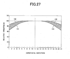
- Fig. 27 shows an example of relative brightness distribution characteristics in horizontal direction of a screen in a display device having a cathode-ray tube.
- the length in horizontal direction is divided equally to 20, and the relative brightness distribution in horizontal direction is shown with the brightness at the center (the position with a scale of 11 in the figure) being scaled to 100.
- the brightness provided by a cathode-ray tube at both sides is in a range of 65 (relative brightness distribution characteristic 101 in the figure) to 85 (relative brightness distribution characteristic 102 in the figure), which is relatively low, compared with the brightness of 100 at the center.
- the deflection center of an electron beam through a horizontal and vertical deflection circuit of a cathode-ray tube is located before the center of the curvature of a screen, and the distance from the deflection center of the cathode-ray tube is longer at the peripheral portion of the screen.
- the brightness at the central portion of the screen and in the vicinity thereof is relatively higher than the brightness of the peripheral portion of the screen, enabling to render images within the functional visual field, that are not uncomfortable for a man and that do not make a man easily get tired.
- a backlight unit is used as the unit to illuminate an object such as a liquid crystal display panel.
- a liquid crystal display device two types of structures have been adapted: direct type and edge light type (light guide plate type) backlight units.
- the direct type backlight unit is a system arranging fluorescent tubes and/or LEDs (Light Emitting Diodes) that are the light sources disposed directly under the liquid crystal panel that is an object, and sufficient brightness can be obtained by increasing the number of light sources in accordance with the screen size of the display device. However, uneven brightness is easily caused between the portions where light sources are disposed and the other portions where light sources are not disposed.
- strength of the backlight unit is required to be attained.
- a structure having a backlight unit enclosure formed by a metal plate, a reflective sheet applied on the inner surface of the backlight, and a plurality of straight tube lamps arranged thereon has been employed.
- the edge light type backlight unit is a system where light sources such as fluorescent lamps are arranged at the edge portion of a light guiding body made from transparent acrylic plate or another, so that one single panel is formed as the surface light source by utilizing multiple reflection within the light guiding body.
- a reflector is disposed behind strip lamps or L-shaped lamps.
- the display device using the edge light type backlight unit can reduce the thickness, however, the mass of the light guiding body becomes excessively large with a large model, and the brightness on the screen becomes difficult to be attained as the screen gets larger.
- a liquid crystal display device wherein the clearance between fluorescent tubes is smaller at the central portion of the screen, and is getting larger toward the edges (for example, see Patent Document 1), in order to achieve lower power consumption, compactness, thinness and lightness.
- the device is so designed as to decrease the number of backlight fluorescent tubes by reducing the brightness gradually from the center of a screen toward the edges, while brightness is maintained at a level a man cannot recognize the reduction of the brightness.
- a backlight illuminating a liquid crystal panel wherein the brightness is maximum at a position above or below the center and is gradually reduced in the vertical direction (for example, see Patent Document 2). This is achieved by controlling the brightness distribution of the backlight through adjustment of a reflector or control of the open width of the color filter.
- Yet another backlight unit is disclosed, wherein the uniformity of the surface light source brightness is maintained by setting the clearance between straight tube type lamps at the central portion of the display screen of a liquid crystal panel smaller, and wider toward the edges of the display screen, thereby achieving lower power consumption (for example, see Patent Document 3).
- the backlight units disclosed in the above-mentioned Patent Documents 1 and 3 are designed to reduce power consumption by reducing the number of fluorescent lamps constituting a backlight while maintaining the uniformity of brightness on the display screen.
- the backlight unit disclosed in Patent Document 2 implements uniformity of display by correcting non-uniformity of brightness in vertical direction that is caused by angle-dependent visibility and heat created by the backlight by adjusting the brightness distribution in vertical direction of the screen of a liquid crystal panel.
- the backlight units disclosed in above mentioned Patent Documents 1, 2 and 3 consequently provides brightness distribution on the display surface of a liquid crystal display device, however, this brightness distribution is formed only in the vertical direction of the display screen.
- the backlight units do not implement two-dimensional characteristics in accordance with visual sense characteristics of a man as provided by a display device using a cathode-ray tube, that is, brightness distribution characteristics with gradient being formed at least in the horizontal and vertical directions from the central portion of a screen. Therefore issues of visual uncomfortableness and fatigability for a man have not been improved yet.
- a first technological means of the present invention for a backlight unit to illuminate an object to be illuminated using a light source is characterized in that the backlight unit has brightness gradient forming means for forming brightness gradient in the horizontal and vertical directions on the surface to be illuminated of the object to be illuminated.
- a second technological means of the present invention is the backlight unit according to the first technological means, which is characterized in that the backlight unit has a reflection portion for causing a light from the light source to exit toward a certain direction, the brightness gradient forming means is disposed on the reflection portion, and the brightness gradient is formed in the horizontal and vertical directions on the surface to be illuminated of the object to be illuminated by controlling the reflectance at the reflection portion.
- a third technological means of the present invention is the brightness gradient forming means according to the second technological means, wherein the brightness gradient forming means is characterized in that the reflection portion has a region where reflectance is relatively higher and another region where reflectance is relatively lower, and brightness gradient is formed in the horizontal and vertical directions on the surface to be illuminated of the obj ect to be illuminated utilizing the reflectance differences.
- a fourth technological means of the present invention is the brightness gradient forming means according to the third technological means, wherein the brightness gradient forming means is characterized in that the means has reflectance gradient formed by changing the reflectance on the reflection portion little by little or step by step; the reflectance gradient is arranged so that the brightness of the central portion is relatively higher than the brightness at the peripheral portion on the surface to be illuminated of the object to be illuminated.
- a fifth technological means of the present invention is the brightness gradient forming means according to the fourth technological means, wherein the brightness gradient forming means is characterized in that the means is a dot pattern provided on the reflection portion, by which the reflectance of the reflection portion is controlled.
- a sixth technological means of the present invention is a technological means according to the fifth technological means which is characterized in that the reflectance of the reflection portion having the dot pattern is controlled by any of the reflectance of each group of fine dots constituting the dot pattern, the density of dots, the shape of dots and/or color of dots, or any combination thereof.
- a seventh technological means of the present invention is a technological means according to the fifth or sixth technological means, which is characterized in that the distribution of the fine dots constituting the dot pattern has a substantially elliptical shape.
- An eighth technological means of the present invention is the technological means according to the first technological means which is characterized in that the backlight unit has a reflection portion for causing the light from the light source to exit in a certain direction, the reflection portion comprises at least a first and second reflection layers each having a predetermined light reflectance and transmittance, the brightness gradient forming means comprises the reflection portion having a first region with the first and second reflection layers being overlapped in the light incident direction and a second region having the first reflection layer only, and brightness gradient is formed in the horizontal and vertical directions on the surface to be illuminated of the object to be illuminated by controlling the reflectance of the reflection portion using the first region providing a relatively higher reflectance and the second region providing a lower reflectance than the first region.
- a ninth technological means of the present invention is the technological means according to the first technological means which is characterized in that the backlight unit has a reflection portion for causing the light from the light source to exit in a certain direction, the reflection portion comprises at least a first and second reflection layers having a predetermined light reflectance and transmittance, the brightness gradient forming means comprises the reflection portion having a first region with the first and second reflection layers that are overlapped in the light incident direction at a position equivalent to the central portion in the horizontal direction of the surface to be illuminated and a second region with the first reflection layer only at both the edge portions, and brightness gradient is formed in the horizontal and vertical directions on the surface to be illuminated of the object to be illuminated by controlling the reflectance of the reflection portion in the horizontal direction of the surface to be illuminated using the first region providing relatively higher reflectance and the second region providing lower reflectance than the first region, and by setting the brightness of the light source located at a position equivalent to the central portion in the vertical direction of the surface to be illuminated relatively higher than the brightness of the light source located at both the
- a tenth technological means of the present invention is the technological means according to the first technological means which is characterized in that the backlight unit has a reflection portion for causing the light from the light source to exit in a certain direction, the reflection portion comprises at least a first and second reflection layers having a predetermined light reflectance and transmittance, the brightness gradient forming means comprises the reflection portion having a first region with the first and second reflection layers that are overlapped in the light incident direction at a position equivalent to the central portion in the vertical direction of the surface to be illuminated and a second region with the first reflection layer only at both the edge portions, and brightness gradient is formed in the horizontal and vertical directions on the surface to be illuminated of the object to be illuminated by controlling the reflectance of the reflection portion in the vertical direction of the surface to be illuminated using the first region providing relatively higher reflectance and the second region providing lower reflectance than the first region, and also by setting the brightness of the light source located at a position equivalent to the central portion in the horizontal direction of the surface to be illuminated relatively higher than the brightness of the light source located
- An eleventh technological means of the present invention is the technological means according to the first technological means which is characterized in that the light source comprises a fluorescent lamp, the brightness gradient forming means is disposed in the glass tube of the fluorescent lamp to form brightness gradient in the horizontal and vertical directions of the surface to be illuminated of the object to be illuminated by controlling the transmittance of the glass tube.
- a twelfth technological means of the present invention is the technological means according to the first technological means which is characterized in that the backlight unit has a diffusion portion that causes the light from the light source to diffuse, the brightness gradient forming means is disposed in the diffusion portion to form brightness gradient in the horizontal and vertical directions of the surface to be illuminated of the object to be illuminated by controlling the transmittance of the diffusion portion.
- a thirteenth technological means of the present invention is the technological means according to the eleventh or twelfth technological means which is characterized in that the brightness gradient forming means has a region in the glass tube or the diffusion portion providing relatively higher transmittance and another region providing lower transmittance and the difference of which forms brightness gradient in the horizontal and vertical directions on the surface to be illuminated of the object to be illuminated.
- a fourteenth technological means of the present invention is the technological means according to the thirteenth technological means which is characterized in that the brightness gradient forming means has transmittance gradient formed by changing the transmittance of the diffusion portion little by little or step by step, brightness at the central portion on the surface to be illuminated of the object to be illuminated is made relatively higher than the brightness at the peripheral portion according to the transmittance gradient.
- a fifteenth technological means of the present invention is the technological means according to any of the eleventh to fourteenth technological means which is characterized in that the brightness gradient forming means is a dot pattern disposed in the glass tube or diffusion portion and that the transmittance is controlled by the dot pattern.
- a sixteenth technological means of the present invention is the technological means according to the fifteenth technological means which is characterized in that the transmittance of the glass tube or diffusion portion provided with the dot pattern is controlled by any of the transmittance of fine dot groups constituting the dot pattern, dot density, dot shape, or dot color, or any combination thereof.
- a seventeenth technological means of the present invention is the technological means according to the sixteenth technological means which is characterized in that the distribution form of fine dots constituting the dot pattern is substantially elliptical.
- An eighteenth technological means of the present invention is the technological means according to the first technological means which is characterized in that the light source comprises a fluorescent lamp, the brightness gradient forming means is provided in a glass tube of the fluorescent lamp, and the brightness gradient is formed in the horizontal and vertical directions on the surface to be illuminated of the object to be illuminated by controlling the brightness on the tubular surface of the glass tube.
- a nineteenth technological means of the present invention is the technological means according to the eighteenth technological means which is characterized in that the brightness gradient forming means optimizes the thickness of the fluorescent substance formed inside of the glass tube of the fluorescent lamp at the position equivalent to the central portion on the surface to be illuminated of the object to be illuminated, and that the brightness of the tubular surface of the glass tube is controlled by increasing or decreasing the thickness at positions equivalent to the peripheral portion on the surface to be illuminated of the object to be illuminated from the optimized thickness.
- a twentieth technological means of the present invention is the technological means according to the first technological means which is characterized in that the light source comprises LEDs, the LEDs are disposed with a substantially uniform density in each of the regions formed on the substrate of the backlight unit, the brightness gradient forming means forms brightness gradient in the horizontal and vertical directions on the surface to be illuminated of the obj ect to be illuminated by controlling the radiation brightness or radiation wavelength of the LEDs.
- a twenty-first technological means of the present invention is the technological means according to the twentieth technological means which is characterized in that the brightness of the LEDs differs among regions that are concentrically formed around the central portion of the substrate of the backlight unit and in the vicinity thereof.
- a twenty-second technological means of the present invention is the technological means according to the first technological means which is characterized in that the light source comprises LEDs, the LEDs have substantially same brightness, and the brightness gradient forming means forms brightness gradient in the horizontal and vertical directions on the surface to be illuminated of the obj ect to be illuminated by controlling the surface density of the LEDs in each of regions formed on the substrate of the backlight unit.
- a twenty-fourth technological means of the present invention is a liquid crystal display device which is characterized in that the device has the backlight unit implemented by any of the first through twenty-third technological means and a liquid crystal panel to be illuminated by the backlight unit.
- a twenty-fifth technological means of the present invention is characterized in that a liquid crystal display device which carries out image rendering by radiating the illumination light on a liquid crystal panel has brightness gradient forming means to form brightness gradient in the horizontal and vertical directions on the display screen of the liquid crystal panel.
- a twenty-sixth technological means of the present invention is the technological means according to the twenty-fifth technological means which is characterized in that the brightness gradient forming means has a gradation conversion portion which carries out predetermined gradation conversion processes for input image data and a control portion which controls gradation conversion characteristics in the gradation conversion portion by switching depending on the input image data, and that the control portion switches the gradation conversion characteristics for the gradation conversion portion depending on the position of the image data in the display screen, thereby forming brightness gradient in the horizontal and vertical directions on the display screen of the liquid crystal panel.
- a twenty-seventh technological means of the present invention is the technological means according to the twenty-fifth technological means which is characterized in that the liquid crystal panel of the brightness gradient forming means is structured to have an aperture ratio that is determined in accordance with the position in a display screen, and that brightness gradient is formed in the horizontal and vertical directions on the display screen of the liquid crystal panel by changing the aperture ratio.
- a twenty-eighth technological means of the present invention is the technological means according to any of the twenty-fifth to twenty-seventh technological means which is characterized in that the display screen of the liquid crystal panel has an aspect ratio of 16:9.
- the horizontal and vertical directions in this specification mean the two directions perpendicular to the optical axis of the light source on the screen (the surface to be illuminated) of a liquid crystal panel.
- the brightness gradient forming means to be provided for the backlight unit forms brightness gradient at least in the horizontal and vertical directions so that the brightness at the central portion of the screen and in the vicinity thereof is relatively higher than the brightness at the peripheral portion of the screen, just like a display device using a cathode-ray tube, by:
- the brightness gradient forming means to be provided with a liquid crystal display device forms brightness gradient at least in the horizontal and vertical directions so that the brightness at the central portion of the screen and in the vicinity thereof is relatively higher than the brightness at the peripheral portion of the screen, just like a display device using a cathode-ray tube, by:
- brightness gradient forming means to form brightness gradient at least in the horizontal and vertical directions on the display screen (the liquid crystal panel) is provided for a reflection layer disposed in a backlight unit, so that the brightness at the central portion of the screen and in the vicinity thereof is relatively higher than the brightness at the peripheral portion of the screen, just like a display device using a cathode-ray tube.
- This brightness gradient forming means in this embodiment is provided for the purpose of controlling reflectance of the light from a light source.
- Figs 1A and 1B are the drawings for explaining an embodiment of a direct-lighting backlight unit of the present invention.
- a schematic plan view showing the internal structure of the backlight unit is shown in Fig. 1A while a schematic structural view of the backlight unit, illustrating cross-section A-A of Fig. 1A is shown in Fig. 1B.
- reference numeral 10 denotes a backlight unit
- 11 denotes a fluorescent lamp
- 12 denotes an enclosure
- 13 denotes a reflection layer disposed at the bottom of the enclosure
- 14 denotes a diffusion unit
- 15 denotes a lamp supporting member.
- Fig. 1A shows the internal structure of the unit, the diffusion unit 14 of which shown in Fig. 1B has been removed.
- a backlight unit 10 has a reflection unit to direct the light from the fluorescent lamps 11 toward a certain direction.
- a reflection layer 13 is provided on the inner surface of the bottom of an enclosure 12 of the backlight unit 10.
- This enclosure 12 may be structured by shield plates for shielding electromagnetic waves to be generated from fluorescent lamps 11.
- the reflection layer 13 is retained with a gap against the inner surface of the bottom being maintained, or retained by being directly disposed on the inner surface of the bottom, and the reflection layer 13 may be, for example, a foamed PET (Polyethylene Terephthalate) sheet or materials having a light reflection surface such as silver, aluminum, or another material.
- a foamed PET sheet for example, E60L or E60V type Lumirror (R) supplied by Toray Co. , Ltd. may be preferably used.
- a foamed PET sheet is often used for a direct type reflection unit.
- a foamed PET reflection sheet is made by foaming PET to create fine air bubbles within the sheet, the light that entered in a formed PET sheet is refracted and regressed by air bubbles, will exit to the incident side, again.
- the refraction characteristic between such PET materials and air in air bubbles causes light to be reflected, reducing loss of light, thereby a reflection unit with high reflectance using inexpensive members is obtained.
- the diffusion unit 14 disposed at the front (surface) of the fluorescent lamps 11 comprises a material such as acrylic plate having light diffusing property, diffusing the light directly entered into or re-directed to the front side after being reflected by the reflection layer 13. Further, a functional film or sheet such as reflective polarizing film, prism sheet or ITO sheet may be included between the diffusion unit 14 and a liquid crystal panel (now shown in the figures) when installed in a liquid crystal display device.
- the light transmitted through the diffusion unit 14 illuminates the object to be illuminated (not shown in the figures), such as a liquid crystal panel to be disposed at the front surface side.
- the object to be illuminated such as a liquid crystal panel to be disposed at the front surface side.
- high voltage is applied to the fluorescent lamps 11 by an inverter power supply circuit (not shown in the figures).
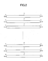
- Fig. 2 is a drawing for explaining an arrangement of fluorescent lamps 11 in the backlight unit applicable to the present invention, showing a plan layout of fluorescent lamps schematically.
- a plurality of fluorescent lamps 11 are arranged parallel in the longitudinal direction.
- the fluorescent lamps 11 are arranged so that the high voltage side H and the low voltage side L of each of fluorescent lamps 11 are aligned to the respective sides, that is, the high voltage side H of a fluorescent lamp 11 is positioned in adjacent to the high voltage side of another fluorescent lamp 11, while the low voltage side L is positioned in adjacent to the low voltage side of another fluorescent lamps 11.
- brightness gradient forming means is provided for the reflection layer 13 in order to form brightness gradient at least in the horizontal and vertical directions of the object to be illuminated such as a liquid crystal panel (hereinafter represented by a liquid crystal panel).
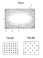
- Fig. 3 is a drawing showing an example of dot pattern applied to the reflection layer 13.
- Figs. 4A and 4B are the drawings showing the enlarged views of the dot pattern of the reflection layer 13 shown in Fig. 3, wherein Fig. 4A shows an enlarged region D3 shown in Fig. 3 while Fig. 4B shows enlarged region D1 shown in Fig. 3.
- the dot pattern applied to the reflection layer 13 has an effect to reduce the reflectance of the reflection layer 13, thus the reflectance of a material forming the dot pattern is relatively lower than the reflectance of the surface of the reflection layer.
- the reflection layer 13 has regions D1, D2 and D3 in which the reflectance becomes smaller step by step from the central portion toward the peripheral portion. These regions D1, D2 and D3 are formed to be substantially elliptical shape, having a major axis in the horizontal direction (right to left) and a minor axis in the vertical direction (top to bottom).
- the dot pattern corresponding to the relative brightness distribution of a cathode-ray tube (relative brightness distribution characteristics 101) shown in Fig. 27 is applied to the reflection layer 13.
- the visual sense characteristics of a man that is, visual field range becomes narrower in vertical direction (top to bottom) and wider in horizontal direction (right to left) can be satisfied.
- the dot pattern applied to the reflection layer 13 has regions D1, D2 and D3 from the central portion toward the peripheral portion with their dot densities become larger step by step, in order to reduce reflectance from the central portion to the peripheral portion.
- dots in the dot pattern have the same size, and dot density of the screen of the side closer to the periphery is set to higher.
- the brightness gradient at the central portion of the screen of a liquid crystal panel and in the vicinity thereof is relatively higher than the brightness gradient at the peripheral portion of the screen, just like a display device having a cathode-ray tube, can be achieved by changing the reflectance on the reflection layer 13 step by step from the central portion toward the peripheral portion.
- the reflectance of the reflection layer 13 can be controlled by applying a dot pattern providing lower reflectance compared with the reflection surface of the reflection layer 13, however on the contrary, the reflectance of the reflection layer 13 may be controlled by applying a dot pattern providing higher reflectance compared with the reflection surface of the reflection layer 13. In this case, a dot pattern providing reflectance that becomes relatively higher from the peripheral portion toward the central portion is applied to the reflection layer 13.
- a foamed PET sheet is used for the reflection layer 13, by applying a dot pattern formed by a high reflectance material such as silver or aluminum to the region equivalent to the central portion of the reflection layer 13, a relatively higher brightness gradient at the central portion of the screen of a liquid crystal panel and in the vicinity thereof than the brightness gradient at the peripheral portion of the screen of the liquid crystal panel can be achieved, just like a display device using a cathode-ray tube.
- a high reflectance material such as silver or aluminum
- the dot pattern for controlling reflectance may control reflectance by changing densities of the dots with the same shape as well as by changing the dot shapes (size), and may further combine dot shapes and densities. Further, as reflectance is changed by changing the color of a dot, reflectance may be controlled by combining shape, density and color of a dot.
- shape of each dot in a dot pattern may be a circular, triangular, polygonal, star-shaped, elliptical, and the color of a dot may be gray, dark brown, silver, green, black, white, purple, or another color.
- the dot pattern as described above does not change reflectance step by step as exemplified in Fig. 3; but may be applied with the gradient slightly reducing reflectance from the central portion toward the peripheral portion (or slightly increasing reflectance from the peripheral portion toward the central portion).
- Such reflectance gradient can be achieved by changing either of the shape, size, density, or color, or combination thereof.
- brightness gradient forming means is to apply an ink or dyestuff whose concentration can be changed in order to control the reflectance of the reflection unit step by step or to control the reflectance of the reflection unit so that the reflectance of the reflection unit increases or decreases gradually.
- the change in concentration may be achieved by changing the concentration of the dyestuff or pigment itself, or the apparent concentration may be changed by changing the thickness of a film on which the dyestuff or pigment is applied.
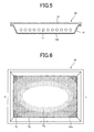
- Fig. 5 is a drawing showing another embodiment of the backlight unit of the present invention, which is a cross-sectional schematic view equivalent to section A-A of the backlight unit shown in Fig. 1A.
- the backlight unit of this embodiment has a reflection surface 12a, instead of a reflection layer 13 of aforementioned Embodiment 1, to reflect the light from fluorescent lamps 11 toward a diffusion unit 14.
- the reflection surface 12a is formed by a reflecting film made of a high reflectance material such as silver or aluminum formed on the inner surface of the bottom of the enclosure 12.
- fluorescent lamps 11 are arranged so that high voltage side H and low voltage side L of each of the fluorescent lamps are aligned respectively to the same sides.
- the brightness gradient forming means for controlling light reflectance as described in Embodiment 1 above is disposed on the reflection surface 12a.
- Fig. 6 is a drawing for explaining an example of a dot pattern applied to the reflection surface 12a.
- the dot pattern applied to the reflection surface 12a has an effect to reduce the reflectance of the reflection surface 12a
- regions D4, D5 and D6 are provided on the reflection surface 12a, and the reflectance of which becomes smaller step by step from the central portion toward the peripheral portion.
- These regions D4, D5 and D6 are formed to be substantially elliptical shapes, having a major axis in the horizontal direction (right to left) and a minor axis in the vertical direction (top to bottom).
- Fig. 7 is a drawing for explaining another structural example of the backlight unit of the present invention, showing a schematic cross-sectional view equivalent to section A-A of the backlight unit shown in Fig. 1A.
- the backlight unit of this embodiment has a reflection layer 13 shown in the structure in Figs. 1A and 1B and a reflection surface 12a shown in Fig. 5.
- fluorescent lamps 11 are arranged so that high voltage side H and low voltage side L of each of the fluorescent lamps are aligned respectively to the same sides.
- a reflection layer 13 is disposed on an enclosure 12 of a backlight unit 10.
- a reflection layer 13 for example, aforementioned foamed PET sheet is used, providing a reflection function to reflect the light from fluorescent lamps 11, however part of the light transmits the reflection layer 13 and exits to the rear side thereof.
- a reflection surface 12a On the inner surface of the bottom of the backlight unit 10, a reflection surface 12a, as described in the above Embodiment 2, is provided, which reflects the light that has transmitted the reflection layer 13 back to the direction of the reflection layer 13. The light reflected by the reflection surface 12a is again separated into reflected light and transmitted light on the reflection layer 13. The transmitted light is directed toward a diffusion unit 14 to be efficiently utilized.
- the reflection layer 13 is supported by a frame-shaped support such as a frame or lamp holder, or a supporting member such as screws or stays.
- the reflection layer 13 does not contact closely with the reflection surface 12a, but air space is provided between the reflection layer 13 and the reflection surface 12a.
- a certain clearance may be provided between the reflection layer 13 and the reflection surface 12a, or the reflection layer 13 may simply be placed and supported on the reflection surface 12a. That is, the presence of thin film air space on the surface of the rear side of the reflection layer 13 makes the refractive index difference between the reflection layer 13 and the air larger on the surface of the rear side of the reflection layer 13, improving the reflectance of the reflection layer 13.
- a material such as adhesive having a refractive index close to that of the reflection layer 13 is disposed on the rear surface of the reflection layer 13, the segment of light that transmits the reflection layer 13 is increased, affecting the light reflection characteristics.
- the brightness gradient forming means described above may further be applied to both of the reflection layer 13 and the reflection surface 12a, or to the reflection surface 12a only.
- the brightness gradient forming means applied to the reflection surface 12s contributes only to the light transmitted the reflection layer 13, it is required to design a reflectance distribution based on the reflectance of the reflection layer 13 (i.e. transmittance).
- Figs 8A and 8B are drawings showing still another embodiment of the backlight unit of the present invention.
- Fig. 8A is a schematic plane view showing the inside of the backlight unit
- Fig. 8B is a schematic structural view of the backlight unit at cross-section B-B shown in Fig. 8A.
- a backlight unit 10 has reflection layers 13a and 13b.
- Fig. 8A shows the internal structure of the unit from which a diffusion unit 14 has been removed.
- the backlight unit 10 has a reflection unit which directs the light from the fluorescent lamps 11 to a certain direction, and in this embodiment, as the reflection unit, two reflection layers 13a and 13b are disposed on the inner surface of the bottom of an enclosure 12 of the backlight unit 10.
- Each of the reflection layers 13a and 13b has a property like a foamed PET sheet as described above, reflects light in a high reflectance, however, a part of the incident light transmits to the rear side.
- a region W where the reflection layers 13a and 13b are overlapped in the vertical direction (light incident direction), and a region S where only the reflection layer 13b is provided, are set up.
- the reflection layers 13a and 13b let a part of incident light transmit to the rear side.
- the light transmitted the first reflection layer 13a disposed on the front side (fluorescent lamps 11 side) is reflected by the second reflection layer 13b on the rear side, and returned to the first reflection layer 13a side. Then the light transmitted the reflection layer 13a directs toward the diffusion unit 14 to be efficiently utilized.
- the region S where only the second reflection layer 13b exists the light reflected by the reflection layer 13b is efficiently utilized, but the light transmitted the reflection layer 13b dissipates at the rear side thereof. During this, even if the transmitted light is reflected by the inner surface of an enclosure 12 and returned to the reflection layer 13b, the effective utilization ratio is low. Therefore, when the regions W and S are compared, the region W having two reflection layers 13a and 13b overlapped each other provides a relatively higher reflectance than the region S having one reflection layer 13b only.
- the regions W and S are set up so that the area of the second reflection layer 13a on the rear side is larger than the area of the first reflection layer 13b on the front side, however, the area of the first reflection layer 13a may be set larger.
- the reflectance at the central portion can be made relatively higher than that of the peripheral portion to achieve brightness gradient in the horizontal direction of a screen by locating the region W having the two reflection layers 13a and 13b at the region equivalent to the central portion of the screen in the horizontal direction, while the region S having the reflection layer 13b only at the region equivalent to the peripheral portion of the screen in the horizontal direction.
- brightness gradient in the vertical direction of the screen is achieved by increasing the brightness of fluorescent lamps 11 at the positions equivalent to the central portion in the vertical direction of the screen (by setting the driving voltage higher), and by decreasing the brightness of the fluorescent lamps 11 at the positions equivalent to the peripheral portion (the upper and lower ends shown in Fig. 8A).
- Figs. 9A and 9B are drawings for explaining yet another embodiment of the backlight unit of the present invention.
- Fig. 9A is a schematic plane view showing the inside of the backlight unit
- Fig. 9B is a schematic structural view of the backlight unit at cross-section C-C shown in Fig. 9A.
- a backlight unit 10 has reflection layers 13a and 13b.
- Fig. 9A shows the internal structure of the unit from which a diffusion unit 14 has been removed.
- the backlight unit 10 has a reflection unit which directs the light from the fluorescent lamps 11 to a certain direction, and in this embodiment, as the reflection unit, two reflection layers 13a and 13b are disposed on the inner surface of the bottom of an enclosure 12 of the backlight unit 10.
- Each of the reflection layers 13a and 13b has a property like a foamed PET sheet as described above, reflects light in a high reflectance, however, a part of the incident light transmits to the rear side.
- a region W with the reflection layers 13a and 13b being overlapped in the vertical direction (light incident direction), and a region S with only the reflection layer 13b provided are set up.
- the reflectance at the central portion can be made relatively higher than that of the peripheral portion to achieve brightness gradient in the horizontal direction of a screen by locating the region W having the two reflection layers 13a and 13b at the region equivalent to the central portion of the screen in the horizontal direction, while the region S having the reflection layer 13a only at the region equivalent to the peripheral portion of the screen in the horizontal direction as explained in Embodiment 4 shown in Figs. 8A and 8B.
- Embodiment 4 shown in Figs. 8A and 8B The difference from Embodiment 4 shown in Figs.
- brightness gradient in the vertical direction of a screen may be achieved by printing a material that degrades reflectance on the surface of the reflection layers 13a and 13b at positions equivalent to the peripheral portion of the screen (the upper and lower ends shown in Fig. 8A or 9A), or a material that degrades transmittance on the surface of fluorescent lamps 11.
- Figs. 10A and 10B are drawings showing yet another embodiment of the backlight unit of the present invention.
- Fig. 10A is a schematic plane view showing the inside of the backlight unit
- Fig. 10B is a view showing a cross-section along a fluorescent lamp 11 shown in Fig. 10A of the structure, including a diffusion unit 14.
- reference numeral 16 shows a screw to be used as the supporting means for the reflection layers 13a and 13b.
- the fluorescent lamps 11 are arranged so that the high voltage side and the low voltage side of each of the fluorescent lamps 11 are aligned respectively at the same sides.
- the regions W and S are set up so that the area of the second reflection layer 13b on the rear side is larger than the area of the first reflection layer 13a on the front side, however, the area of the first reflection layer 13a may be larger.
- the reflectance at the central portion (region W) is made relatively higher than that of the peripheral portion by setting up a region W comprising the two reflection layers 13a and 13b for only the region equivalent to the central portion in the horizontal and vertical directions of the screen, thereby brightness gradient in the horizontal and vertical directions of the screen is achieved.
- a half mirror may be used, for example.
- the transmittance of the light that is reflected by the second reflection layer 13b and returned to the first reflection layer 13a (half mirror) can be improved, thereby achieving a high reflectance.
- the brightness gradient forming means described in Embodiment 1 to Embodiment 3 may be used in combination with the two-layer structure consisting of the reflection layers 13a and 13b. In this embodiment, a structure using two reflection layers is described, however, more than two reflection layers may be provided.
- a retaining element is preferably provided for each of reflection layers 13a and 13b, especially for the first reflection layer 13a located at the front side to provide retaining stability.
- a through-hole is provided to each of the enclosure 12, first reflection layer 13a and second reflection layer 13b, and a screw 16 is inserted into these through-holes to retain reflection layers 13a and 13b on the inner surface of the enclosure 12, thereby maintaining the shapes by preventing the reflection layers 13a and 13b from bending due to gravity, or another force.
- any known means that enables the reflection layers 13a and 13b to be retained on the inner surface of the enclosure can be used besides the screw.
- the retaining means may be provided with the function to retain the reflection layers 13a and 13b as well the function to retain the fluorescent lamps 11.
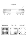
- Fig. 11 is a drawing for explaining another embodiment of the backlight unit of the present invention, showing a schematic plane view of a fluorescent lamp 11.
- brightness gradient forming means for forming brightness gradient at least in the horizontal and vertical directions of a display screen is provided on the glass tube constituting the fluorescent lamp 11.
- the brightness gradient forming means provided here does not control reflectance as provided in the embodiments described above, but controls light transmittance of the glass tube of the fluorescent lamp 11, however, the technological concept attempting to form brightness gradient by controlling the amount of exiting light to the object to be illuminated is shared.
- Figs. 12A, 12B and 12C are the enlarged views showing the dot pattern printed on the glass tube shown in Fig. 1.
- the enlarged view of region D 13 shown in Fig. 11 is shown in Fig.
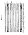
- Fig. 13 shows a dot pattern example which is formed when the fluorescent lamps 11 with the dot pattern being printed are disposed at predetermined positions in the backlight unit.
- a dot pattern for reducing light transmittance of the glass tube is used as the brightness gradient forming means.
- three regions D 11 , D 12 and D 13 with different dot densities are provided so that dot density becomes higher step by step from the central portion of the fluorescent lamp 11 toward the both ends.
- the regions D 11 , D 12 and D 13 formed by these fluorescent lamps 11 are, as shown in Fig. 13, substantially elliptical, having a major axis in the horizontal direction (right to left) and a minor axis in the vertical direction (top to bottom).
- the dot pattern corresponding to the relative brightness distribution of the cathode-ray tube (relative brightness distribution characteristics 101) shown in Fig. 27 is applied to the glass tubes of the fluorescent lamps 11.
- the dot pattern to be applied to the glass tubes of the fluorescent lamps 11 is arranged so that the dot density of the applied regions D 11 , D 12 and D 13 in the dot pattern is increased step by step from the central portion to the both ends for reducing the transmittance of the fluorescent lamps 11 from the central portion to the both ends.
- the dot density of the applied regions D 11 , D 12 and D 13 in the dot pattern is increased step by step from the central portion to the both ends for reducing the transmittance of the fluorescent lamps 11 from the central portion to the both ends.
- the dot density of the applied regions D 11 , D 12 and D 13 in the dot pattern is increased step by step from the central portion to the both ends for reducing the transmittance of the fluorescent lamps 11 from the central portion to the both ends.
- the dot pattern for controlling transmittance as described above may control transmittance by changing density of dots with the same shape or by changing the shape (size) of dots, as the example shown in Fig. 11, and further by changing both of dot shape and density in combination.
- the color of a dot may be changed to change transmittance.
- the shape of each dot in a dot pattern may be a circular, triangular, polygonal, star-shaped, elliptical, and the color of a dot may be gray, dark brown, silver, green, black, white, purple, or another color.
- the dot pattern described above may obtain gradient by reducing transmittance little by little from the central portion toward the peripheral portion of the fluorescent lamps 11 and not by changing transmittance step by step as exemplified in Fig. 11.
- Such transmittance gradient can be achieved by changing either of the shape, size, density, or color, or any combination of these.
- the dot pattern to be applied to the surface of a glass tube can be formed by applying ink on the glass tube by printing such as screen printing or inkjet printing. Besides printing, sputtering or vapor deposition, photolithography or optical machining using a laser beam, or lamination of transparent film having a dot pattern may be used to form a dot pattern.
- ink or dyestuff whose concentration changes can be applied to the glass tube in order to control the transmittance so that the transmittance decreases or increases step by step or gradually.
- the change in concentration may be achieved by changing the concentration of the dyestuff or pigment itself, or by changing apparent concentration caused by the change in the thickness of the film on which the ink or dyestuff is applied.
- a plurality of materials with different transmittances may be applied on the surface of the glass tube. Further, roughness of the surface of the glass tube may be changed to control transmittance based on differences of the optical diffusion characteristic or the optical absorption characteristic of the surface.
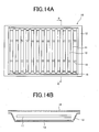
- Figs. 14A and 14B are drawings showing another embodiment of the backlight unit of the present invention.
- Fig. 14A is a schematic plane view showing the inside of the backlight unit
- Fig. 14B is a drawing showing a cross-section along D-D of Fig. 14A depicting a structure including a diffusion unit 14.
- fluorescent lamps 11 are arranged in the vertical direction in parallel with each other, and the high voltage side H and low voltage side L of each of the fluorescent lamps 11 are aligned respectively to the same sides.
- Fig. 15 is a drawing showing another exemplified dot pattern to be formed when fluorescent lamps 11 with a dot pattern being printed are disposed at predetermined positions in the backlight unit.
- a dot pattern that causes to reduce light transmittance of a glass tube is used as brightness gradient forming means.
- regions D 21 , D 22 and D 23 having dot patterns with three different densities are provided so that the dot density becomes larger step by step from the central portion to the both ends of a fluorescent lamp 11.
- the regions D 21 , D 22 and D 23 formed by these fluorescent lamps 11 have, as shown in Fig. 15, substantially elliptical shape, having a major axis in the horizontal direction (right to left) and a minor axis in the vertical direction (top to bottom).
- the dot pattern corresponding to the relative brightness distribution of the cathode-ray tube (relative brightness distribution characteristics 101) shown in Fig. 27 is applied to the glass tubes of the fluorescent lamps 11. This way, even when the fluorescent lamps 11 are vertically arranged, similar brightness gradient can be obtained as when the fluorescent lamps 11 are horizontally arranged.
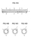
- Figs. 16A to 16D are drawings for explaining another embodiment of the backlight unit of the present invention.
- a schematic cross-sectional view of the backlight unit is shown in Fig. 16A
- the schematic cross-sectional views of a fluorescent lamp 11 at positions B, C and D in Fig. 16A are shown in Figs. 16B, 16C and 16D respectively.
- reference numeral 11a denotes a glass tube constituting a fluorescent lamp
- 11b denotes a fluorescent substance provided on the inner surface of the glass tube
- d denotes the film thickness of the fluorescent substance.
- the brightness gradient described above is formed by changing the film thickness d of the fluorescent substance 11b to be formed on the inner side of the glass tube 11a of a fluorescent lamp in the longitudinal direction of the fluorescent lamp 11.
- the property that tubular surface brightness changes in accordance with the film thickness d of the fluorescent substance 11b is used and radiation brightness gradient is achieved in the longitudinal direction of the fluorescent lamp 11 by changing the film thickness d of the fluorescent substance 11b in accordance with the position in the longitudinal direction of the fluorescent lamp 11.
- the film thickness d of the fluorescent substance 11b of the fluorescent lamb 11 equivalent to the central portion of the screen is set to an optimum film thickness providing the highest brightness, and the film thickness d is set higher or lower toward the high voltage side H or low voltage side L.
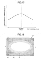
- Fig. 17 is a chart showing an example of the relationship between film thickness d of a fluorescent substance and tubular surface brightness (radiation brightness).
- film thickness d of a fluorescent substance generally changes brightness at turn-on in accordance with the film thickness d of the fluorescent substance.
- An optimum value of the film thickness d for the light to be emitted most brightly exists. That is, as shown in Fig. 17, the light gets dark due to insufficient amount of fluorescent substance when the film thickness d is smaller than the optimum value, on the contrary, the light gets dark due to diffusion of light within the film when the film thickness d gets greater than the optimum value.
- the film thickness d of the fluorescent substance 11b is changed by setting the film thickness d of the fluorescent substance to the optimum film thickness that provides the highest brightness at the substantially central portion of the fluorescent lamp 11 and by increasing or decreasing the film thickness d toward the high voltage side H or low voltage side L at the either ends. In doing so, brightness is reduced either when the film thickness d gets greater than or smaller than the optimum value as described above, and by utilizing this characteristics, brightness gradient is formed on each of the fluorescent lamps 11, to form brightness gradient at least in the horizontal and vertical directions of a display screen.
- the method applying brightness gradient forming means to a glass tube itself of a fluorescent lamp T1 can be applied not only to the straight tube type fluorescent lamps but U-shaped, block C-shaped and L-shaped fluorescent lamps.
- Fig. 18 is a drawing for explaining another embodiment of the backlight unit of the present invention.
- brightness gradient forming means for forming brightness gradient at least in the horizontal and vertical directions of a display screen is provided in a diffusion unit 14.
- a diffusing plate or diffusing sheet having light diffusing function is used as the diffusion unit 14.
- brightness gradient forming means for controlling light transmittance is provided on the surface of such a diffusion unit 14.
- a dot pattern for reducing light transmittance is applied on the surface of the diffusion unit 14.
- regions D 31 , D 32 and D 33 having dot patterns with three different densities are provided so that the dot density becomes larger step by step from the central portion to the peripheral portion of a display screen.
- the regions D 31 , D 32 and D 33 have substantially elliptical shape and are formed to have a major axis in the horizontal direction (right to left) and a minor axis in the vertical direction (top to bottom).
- the dot pattern corresponding to the relative brightness distribution of the cathode-ray tube (relative brightness distribution characteristics 101) shown in Fig. 27 is applied to a reflection layer 13.
- the backlight unit of the present invention can be applied not only to a direct type backlight unit, but also to an edge light type backlight unit. That is, brightness gradient forming means provided on a reflection layer or reflection surface that constitutes a reflection unit, florescent lamps, and diffusion unit in each of the embodiments described above, is not applicable only to a direct type backlight unit but edge light type backlight unit, and relatively higher brightness can be obtained at the central portion of a liquid crystal panel screen and in the vicinity thereof than the brightness at the peripheral portion of the screen, just like a display device using a cathode-ray tube.
- brightness gradient is formed at least in the horizontal and vertical directions on a display screen and relatively higher brightness can be obtained at the central portion of a display screen of a liquid crystal panel and in the vicinity thereof than the brightness at the peripheral portion of the screen, just like a display device using a cathode-ray tube.
- Fig. 19A is a drawing for explaining an embodiment of a liquid crystal display device of the prevent invention, which shows a schematic cross-sectional structure of a liquid crystal display device having a backlight unit.
- reference numeral 20 denotes a liquid crystal display device
- reference numeral 21 denotes a liquid crystal panel.
- Fig. 19B is a drawing for explaining another embodiment of a liquid crystal display device of the prevent invention, which shows a schematic cross-sectional structure of a liquid crystal display device having a backlight unit but which has a polarizing reflective film 22 provided between the diffusion unit 14 and the liquid crystal panel 21 in addition to the configuration of the liquid crystal display device 20 shown in Fig. 19A.
- the liquid crystal display device 20 is provided with a general liquid crystal panel 21 with liquid crystal material sealed between two transparent insulation substrates, which is the key structural element, and a backlight unit 10 for illuminating light to the liquid crystal panel 21.
- a backlight unit 10 for illuminating light to the liquid crystal panel 21.
- a backlight unit of any of aforementioned Embodiments 1 to 10 can be applied.
- brightness gradient is formed at least in the horizontal and vertical directions of the display screen of the liquid crystal panel 21, thereby achieving a similar brightness distribution characteristics provided by a display device using a cathode-ray tube.
- an aspect ratio of 16:9 is used, for example. Therefore, in a liquid crystal display device of the present invention, the aspect ratio of the display screen may be set to 16:9. In this case, the aspect ratio of the aforementioned reflection layer or reflection surface, and that of the diffusion unit are also set to 16:9. By setting so, an image matching to human visual sense characteristics and providing the feeling of presence can be obtained.
- a liquid crystal display device with high light utilization efficiency can be obtained by providing a polarizing reflective film 22 between a liquid crystal panel 21 and a diffusion unit 14 of a backlight unit 10 in the liquid crystal display device 20 described above.
- the polarization transmission axis of the polarizing reflective film 22 is aligned with the polarization transmission axis of the incident side polarizer of the liquid crystal panel 21.
- the polarizing reflective film 22 enables the illumination light with aligned polarizing direction to be generated efficiently, thereby obtaining a liquid crystal display device with high light utilization efficiency by aligning the deflecting direction of this illumination light to the polarization axis of the polarizer at the incident side.
- a functional film or sheet such as ITO sheet, diffusing film or prism sheet, and another can be provided further.
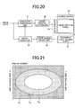
- Fig. 20 is a block diagram of key units showing a schematic structure of the liquid crystal display device of this embodiment.
- Fig. 21 is an illustrative drawing indicating display screen regions in the liquid crystal display device of this embodiment
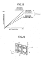
- Fig. 22 is an illustrative drawing showing gradation conversion characteristics (input/output characteristics) of a gradation conversion unit in the liquid crystal display device of this embodiment.
- the liquid crystal display device of this embodiment is provided with a gradation conversion unit 31 carrying out a predetermined gradation conversion process with the input image data, and a liquid crystal controller 32 outputting liquid crystal driving signals to a gate driver 34 and a source driver 35 of a liquid crystal panel 33.
- the liquid crystal display device is also provided with a microcomputer 36 controlling a light source driver unit 38 for switching and controlling gradation conversion characteristics at the gradation conversion unit 31 based on the synchronization signal of the input image data, and for driving a backlight light source (fluorescent lamps) 37.
- the microcomputer 36 determines the position on the screen where the image data is displayed based on the synchronization signal of the input image data, then outputs an instruction to the gradation conversion unit 31 to switch gradation conversion characteristics of the gradation conversion unit 31 in accordance with the position on the screen.
- the display screen is divided into region D 41 equivalent to the central portion of the display screen, region D 42 equivalent to the peripheral portion thereof, and region D 43 equivalent to the most peripheral portion, and gradation conversion characteristics for the data is switched based on the information regarding either of divided regions D 41 , D 42 or D 43 the data is to be displayed.
- the gradation conversion unit 31 has a gradation conversion characteristic a that outputs an input gradation level as it is (with no conversion being carried out), a gradation conversion characteristic b that outputs an input gradation level after being slightly suppressed, and a gradation conversion characteristic c that outputs an input gradation level after being further suppressed, wherein these characteristics are switchable.
- LUT look-up table
- the microcomputer 36 outputs a control signal to the gradation conversion unit 31 to select the gradation conversion characteristic a when the screen position of the image data to be displayed belongs to the region D 41 on the display screen. That is, the gradation conversion characteristic a is selected for the image data to be displayed in the region D 41 on the display screen, they are outputted on the liquid crystal controller 32 as they are (with no conversion being carried out).
- the microcomputer 36 outputs a control signal to the gradation conversion unit 31 to select the gradation conversion characteristic b when the screen position of the image data to be displayed belongs to the region D 42 on the display screen.
- the gradation conversion characteristic b is selected and the gradation conversion process is carried out for the image data to be displayed in the region D 42 on the display screen, thus the display brightness in the region D 42 on the display screen is slightly reduced.
- the microcomputer 36 outputs a control signal to the gradation conversion unit 31 to select the gradation conversion characteristic c when the screen position of the image data to be displayed belongs to the region D 43 on the display screen. That is, the gradation conversion characteristic c is selected and the gradation conversion process is carried out for the image data to be displayed in the region D 43 on the display screen, thus the display brightness in the region D 43 on the display screen is further reduced.
- the light transmittance of the liquid crystal panel 33 at the peripheral portion on the display screen is reduced (display brightness is reduced), compared with the light transmittance at the central portion, thereby achieving a similar brightness distribution provided by a display device using a cathode-ray tube.
- display brightness is reduced
- gradation level of the image data according to the screen position of the image data to be displayed, brightness gradient at least in the horizontal and vertical directions can be achieved so that the peripheral portion of the display screen is darker than the central portion.
- the display screen is divided into three regions of D 41 , D 42 , and D 43 , which are concentrically and elliptically formed, and gradation conversion characteristics a, b, or c for image data to be displayed in each of divided regions D 41 , D 42 , and D 43 is selected and switched; however, it will be understood without mentioning that the number of regions into which the display screen is divided and the positions of divided regions can be changed as necessary in accordance with a display screen size or aspect ratio.
- the brightness gradient may be achieved at least in the horizontal and vertical directions of a display screen by varying the reference gradation voltage for driving a liquid crystal panel according to a display screen position on a liquid crystal panel.
- the brightness gradient may be achieved in the horizontal and vertical directions of a display screen by changing aperture ratio according to a display screen position on a liquid crystal panel. That is, the amount of light that transmits a liquid crystal panel can be increased by setting the aperture ratio at the central portion of the screen of the liquid crystal panel to a greater value, while the amount of light that transmits the liquid crystal panel can be decreased by setting the aperture ratio at the peripheral portion of the screen of the liquid crystal panel to a smaller value.
- the brightness distribution can be formed in which the central portion of the display screen becomes brighter than the peripheral portion thereof, just like a display device using a cathode-ray tube.
- Fig. 23 is a drawing showing an exemplified structure for controlling the aperture ratio of a liquid crystal panel, wherein reference numeral 21 denotes the liquid crystal panel, reference numeral 41 denotes a light shielding film, reference numeral 42 denotes a transparent electrode, reference numeral 43 denotes a TFT driver element, i denotes incident light for the liquid crystal panel, and o denotes the light exiting from the liquid crystal panel.
- a shielding film 41 generally usingmeshedmetal film is provided on a liquid crystal panel 21.
- brightness gradient is formed based on the light transmittance of each pixel by controlling the aperture ratio of each pixel provided by the light shielding film 41 in forming the light shielding film 41, so that brightness gradient is formed at least in the horizontal and vertical directions of the display screen, thereby obtaining a brighter display screen at the central portion than the peripheral portion of the display screen, just like a display device using a cathode-ray tube.
- Fig. 24A is a drawing for explaining another embodiment of the liquid crystal display device (or backlight unit) of the present invention, showing a schematic cross-sectional structure of the liquid crystal display device having a backlight unit with LEDs as the light source.
- reference numeral 50 denotes a liquid crystal display device, and the liquid crystal display device 50 has a circuit substrate 51 with a control circuit mounted thereon, a rim 52 supporting the liquid crystal panel, a liquid crystal panel 53, a frame 54 of the backlight unit, a polarizing reflective film 55, point light sources (LED) 56, and also has a diffusion unit 57, which diffuses the light directly entering from a LED 56 or the light going forward after being reflected by the reflection unit 58, provided on the rear side of the LEDs 56.
- the LEDs 56 illuminate the liquid crystal panel 53 disposed at the front side through the diffusion unit 57.
- Fig. 24B is a drawing for explaining another embodiment of the liquid crystal display device (or backlight unit) of the present invention, showing a schematic cross-sectional structure of a liquid crystal display device having a backlight unit.
- fluorescent lamps 59 are provided as the light source to the frame 54 of the backlight unit in addition to the configuration of the liquid crystal display device 50 shown in Fig. 24A.
- the brightness gradient forming means for forming brightness gradient at least in the horizontal and vertical directions of the display screen is achieved by using either radiation brightness, radiation wavelength or surface density of the LEDs which are the point light sources, or any combination thereof.
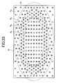
- Fig. 25 is a drawing for explaining an example where LEDs are arranged in the backlight unit of the present invention, so that they have different surface densities in different regions.
- the brightness of the backlight unit can be controlled by the ratio of the area in which an LED is included against the area in which no LED is included, that is, the difference in surface densities of LEDs.
- the brightness gradient forming means of this embodiment forms brightness gradient at least in the horizontal and vertical directions of the display screen by utilizing the differences in the surface densities.
- Figs. 24A and 25 many LEDs 56 with substantially same brightness are provided on the reflection unit 58.
- the four regions D 51 , D 52 , D 53 and D 54 are the regions which are created by dividing the display screen to form concentric ellipses that are substantially symmetric in left-to-right and top-to-bottom directions, and are set sequentially from the central side to the peripheral portion of the display screen.
- the brightness on the display screen is set to be relatively highest by disposing LEDs 56 at high density.
- LEDs 56 are arranged with a density lower than that in region D 51 , then in the region D 53 , which is further outer region, LEDs 56 are arranged with a further lower density. In the most outer region D 54 , LEDs 56 are arranged with the lowest density, thereby decreasing the brightness on the display screen to relatively the lowest. In this way, brightness gradient can be formed in the horizontal and vertical directions of the display screen by changing the density of LEDs 56 with the substantially same brightness for each region.
- a liquid crystal display device with a backlight unit having point light sources such as LEDs 56 can obtain a display characteristics similar to the relative brightness distribution provided by a general display device having a cathode-ray tube.
- the backlight unit of this embodiment as the backlight for a liquid crystal display device, the brightness by the LEDs becomes lower and lower toward the peripheral portion, thereby making the central portion relatively brighter and the peripheral portion darker as a whole backlight unit, and a display device having brightness distribution similar to the brightness distribution characteristics of a cathode-ray tube can be obtained.
- Fig. 26 is a drawing for explaining an example where LEDs are arranged so that LEDs in each of the regions in the backlight unit of the present invention have different radiation brightness.
- the brightness of the backlight unit can be controlled by the difference in the radiation brightness or radiation wavelength, when the surface density of LEDs is the same.
- the brightness gradient forming means in this embodiment forms brightness gradient at least in the horizontal and vertical directions of the display screen by utilizing the differences in the radiation brightness or radiation wavelength.
- Figs. 24A and 26 many LEDs 56 with different radiation brightness are provided in each of the regions on a reflection unit 58.
- the four regions D 61 , D 62 , D 63 and D 64 are the regions which are created by dividing the display screen to form concentric ellipses that are substantially symmetric in left-to-right and top-to-bottom directions, and are set up sequentially from the central side to the peripheral portion of the display screen.
- LEDs 56 with the high radiation brightness are disposed to set the brightness on the display screen relatively the highest.
- LEDs 56 with a lower radiation brightness are disposed, then in the region D 63 , and D 64 which is further outer regions, LEDs 56 having a more lower radiation brightness and a further lower radiation brightness respectively are disposed.
- LEDs 56 with the lowest radiation brightness are disposed, to set the brightness on the display screen relatively the lowest. This way, brightness gradient in the horizontal and vertical directions of the display screen can be formed by changing the radiation brightness of LEDs with substantially the same density.
- the density of LEDs 56 which are the light source is substantially the same and the brightness of LEDs 56 becomes lower from the central portion (region D 61 ) toward the peripheral portion (D 62 , D 63 , D 64 ) of the backlight unit.
- the brightness of LEDs 56 can be adjusted, for example, by the difference in dominant radiation wavelength within the visible light wavelength region (difference in brightness of R, G or B), and by the difference in voltages to be applied to the LEDs in the visible light wavelength region.
- the brightness of LEDs 56 may also be controlled by varying the duty ratio of dimmer signals for a LED turn-on circuit. The brightness may be adjusted by disposing a filter in front of LEDs.
- fluorescent lamps 59 may be added as the light source together with LEDs 56.
- LEDs 56 and fluorescent lamps 59 are arranged so that the brightness for the darkest peripheral portion is secured by fluorescent lamps 59, while the brightness for the brightest central portion is secured by LEDs 56.
- LEDs 56 By using LEDs 56, the brightness of the whole screen is also improved.
- fluorescent lamps 59 may have, for example, partial uneven brightness which reflects the shape of a fluorescent lamp, and also intrinsic uneven brightness in the longitudinal direction of a linear fluorescent lamp, however, such uneven brightness can be solved by using LEDs 56.
- a desirable brightness distribution can be obtained by adjusting brightness distribution of fluorescent lamps 59 which are the linear light sources by using radiation brightness or surface density of LEDs 56 which are the point light source.
- the backlight unit with the brightness gradient forming means for forming brightness gradient at least in the horizontal and vertical directions so that relatively higher brightness can be obtained at the central portion of a display screen and in the vicinity thereof than the brightness at the peripheral portion of the screen of the liquid crystal panel to be illuminated by the light source constituting the backlight unit
- a backlight unit with brightness distribution characteristics providing relatively higher brightness at the central portion of the screen and in the vicinity thereof than at peripheral portion of the screen just like a display device using a cathode-ray tube, can be obtained.
- a liquid crystal display device with brightness distribution characteristics providing relatively higher brightness at the central portion of the screen and in the vicinity thereof than at peripheral portion of the screen can be obtained.
- a liquid crystal display device with brightness distribution characteristics providing relatively higher brightness at the central portion of the screen and in the vicinity thereof than at peripheral portion of the screen, just like a display device using a cathode-ray tube, can be obtained.
Landscapes
- Physics & Mathematics (AREA)
- Nonlinear Science (AREA)
- General Physics & Mathematics (AREA)
- Crystallography & Structural Chemistry (AREA)
- Chemical & Material Sciences (AREA)
- Optics & Photonics (AREA)
- Mathematical Physics (AREA)
- Engineering & Computer Science (AREA)
- Theoretical Computer Science (AREA)
- Computer Hardware Design (AREA)
- Liquid Crystal (AREA)
- Planar Illumination Modules (AREA)
- Devices For Indicating Variable Information By Combining Individual Elements (AREA)
Abstract
Description
Claims (28)
- A backlight unit for illuminating an object to be illuminated using a light source, wherein the backlight unit comprises brightness gradient forming means for forming brightness gradient in the horizontal and vertical directions on a surface to be illuminated of the.object to be illuminated.
- The backlight unit of claim 1, wherein the backlight unit has a reflection portion for causing the light from the light source to exit toward a certain direction, wherein the brightness gradient forming means is provided on the reflection portion, and wherein brightness gradient in the horizontal and vertical directions on the surface to be illuminated of the object to be illuminated is formed by controlling the reflectance at the reflection portion.
- The backlight unit of claim 2, wherein the brightness gradient forming means has a region providing relatively higher reflectance and another region providing relatively lower reflectance at the reflection portion, and wherein brightness gradient in the horizontal and vertical directions on the surface to be illuminated of the object to be illuminated is formed by the difference in the reflectance.
- The backlight unit of claim 3, wherein the brightness gradient forming means has reflectance gradient whose reflectance changes little by little or step by step at the reflection portion, and wherein relatively higher brightness is obtained at the central portion on the surface to be illuminated of the object to be illuminated and in the vicinity thereof than at peripheral portion by the reflectance gradient.
- The backlight unit of claim 4, wherein the brightness gradient forming means is a dot pattern provided on the reflection portion, and wherein the reflectance of the reflection portion is controlled by the dot pattern.
- The backlight unit of claim 5, wherein the reflectance of the reflection portion provided with the dot pattern is controlled by any of the reflectance of a group of fine dots constituting the dot pattern, dot density, dot shape and dot color, or any combination thereof.
- The backlight unit of claim 5 or 6, wherein the distribution of the fine dots constituting the dot pattern has a substantially elliptical shape.
- The backlight unit of claim 1, wherein the backlight unit has a reflection portion for causing the light from the light source to exit toward a certain direction, wherein the reflection portion comprises at least a first and a second reflection layers having a predetermined level of light reflectance and transmittance, wherein the brightness gradient forming means has the reflection portion consisting of a first region with the first and second reflection layers being overlapped in the incident direction of light and a second region consisting of the first reflection layer only, and wherein brightness gradient is formed in the horizontal and vertical directions on the surface to be illuminated of the object to be illuminated by controlling reflectance of the reflection portion using the first region with relatively higher reflectance and the second region with lower reflectance than the first region.
- The backlight unit of claim 1, wherein the backlight unit has a reflection portion for causing the light from the light source to exit toward a certain direction, wherein the reflection portion comprises at least a first and a second reflection layers having a predetermined level of light reflectance and transmittance, wherein the brightness gradient forming means has the reflection portion consisting of a first region with the first and second reflection layers being overlapped in the incident direction of light located at a position equivalent to the central portion in the horizontal direction on the surface to be illuminated, and a second region consisting of the first reflection layer only located at the both ends, and wherein brightness gradient is formed in the horizontal and vertical directions on the surface to be illuminated of the obj ect to be illuminated by controlling reflectance of the reflection portion in the horizontal direction on the surface to be illuminated and also by making the brightness of the light source located at the position equivalent to the central portion in the vertical direction on the surface to be illuminated relatively higher than the brightness of the light sources located at the both ends, using the first region with relatively higher reflectance and the second region with lower reflectance than the first region.
- The backlight unit of claim 1, wherein the backlight unit has a reflection portion for causing the light from the light source to exit toward a certain direction, wherein the reflection portion comprises at least a first and a second reflection layers having a predetermined level of light reflectance and transmittance, wherein the brightness gradient forming means has the reflection portion consisting of a first region with the first and second reflection layers overlapped in the incident direction of light located at a position equivalent to the central portion in the vertical direction on the surface to be illuminated and a second region consisting of the first reflection layer only located at the both ends, and wherein brightness gradient is formed in the horizontal and vertical directions on the surface to be illuminated of the object to be illuminated by controlling reflectance of the reflection portion in the vertical direction on the surface to be illuminated and also by making the brightness of the light source located at the position equivalent to the central portion in the horizontal direction on the surface to be illuminated relatively higher than the brightness of the light sources located at the both ends, using the first region with relatively higher reflectance and the second region with lower reflectance than the first region.
- The backlight unit of claim 1, wherein the light source comprises a fluorescent lamp, wherein the brightness gradient forming means is provided on the glass tube of the fluorescent lamp, and wherein brightness gradient is formed in the horizontal and vertical directions on the surface to be illuminated of the object to be illuminated by controlling the transmittance of the glass tube.
- The backlight unit of claim 1, wherein the backlight unit has a diffusion portion for diffusing the light from the light source, wherein the brightness gradient forming means is provided on the diffusion portion, and wherein brightness gradient is formed in the horizontal and vertical directions on the surface to be illuminated of the obj ect to be illuminated by controlling the transmittance at the diffusion portion.
- The backlight unit of claim 11 or 12, wherein the brightness gradient forming means has a region providing relatively higher transmittance and another region providing relatively lower transmittance at the glass tube or the diffusion portion, and wherein brightness gradient is formed in the horizontal and vertical directions on the surface to be illuminated of the obj ect to be illuminated by the difference in the transmittance.
- The backlight unit of claim 13, wherein the brightness gradient forming means has transmittance gradient in which the transmittance at the glass tube or the diffusion portion changes little by little or step by step, and wherein brightness at the central portion on the surface to be illuminated of the object to be illuminated is made relatively higher than the brightness at the peripheral portion according to the transmittance gradient.
- The backlight unit of any of claims 11 to 14, wherein the brightness gradient forming means is a dot pattern provided on the glass tube or the diffusion portion, and wherein the transmittance is controlled by the dot pattern.
- The backlight unit of claim 15, wherein the transmittance of the glass tube or the diffusion portion provided with the dot pattern is controlled by any of the transmittance of a group of fine dots constituting the dot pattern, dot density, dot shape and dot color, or any combination thereof.
- The backlight unit of claim 16, wherein the distribution of the fine dots constituting the dot pattern has a substantially elliptical shape.
- The backlight unit of claim 1, wherein the light source comprises fluorescent lamps, wherein the brightness gradient forming means is provided on the glass tube of the fluorescent lamps, and wherein the brightness gradient is formed in the horizontal and vertical directions on the surface to be illuminated of the object to be illuminated by controlling the tubular surface brightness on the glass tube.
- The backlight unit of claim 18, wherein the brightness gradient forming means controls tubular surface brightness on the glass tube by optimizing the thickness of the fluorescent substance to be formed on the inner side of the glass tube of the fluorescent lamps at the position equivalent to the central portion on the surface to be illuminated of the object to be illuminated, and also by increasing or decreasing the optimized thickness at positions equivalent to peripheral portion on the surface to be illuminated of the object to be illuminated.
- The backlight unit of claim 1, wherein the light source comprises LEDs, wherein the LEDs are arranged with substantially equal surface density in each of the regions formed on the substrate of the backlight unit, wherein the brightness gradient forming means forms brightness gradient in the horizontal and vertical directions on the surface to be illuminated of the object to be illuminated by controlling radiation brightness or radiation wavelength of the LEDs.
- The backlight unit of claim 20, wherein the brightness of the LEDs differs from each other in regions which are concentrically formed around the center of the substrate of the backlight unit.
- The backlight unit of claim 1, wherein the light source comprises LEDs, wherein each of the LEDs has substantially equal brightness, wherein the brightness gradient forming means forms brightness gradient in the horizontal and vertical directions on the surface to be illuminated of the object to be illuminated by controlling the surface density of the LEDs in each of the regions formed on the substrate of the backlight unit.
- The backlight unit of claim 22, wherein the surface density of the LEDs differs from each other in regions which are concentrically formed around the center of the substrate of the backlight unit.
- A liquid crystal display device comprising the backlight unit of any of claims 1 to 23 and a liquid crystal panel to be illuminated by the backlight unit.
- A liquid crystal display device for displaying images by irradiating illumination light from a backlight unit on a liquid crystal panel, wherein the liquid crystal display device has brightness gradient forming means to form brightness gradient in the horizontal and vertical directions on the display screen of the liquid crystal panel.
- The liquid crystal display device of claim 25, wherein the brightness gradient forming means has a gradation conversion portion for carrying out a predetermined gradation conversion process for input image data, and a control portion for controlling switching of gradation conversion characteristics at the gradation conversion portion according to the input image data, and wherein the control portion forms brightness gradient in the horizontal and vertical directions on the display screen of the liquid crystal panel by switching gradation conversion characteristics at the gradation conversion portion based on the display screen position of the image data.
- The liquid crystal display device of claim 25, wherein, as the brightness gradient forming means, the liquid crystal panel is configured to have aperture ratios varied in accordance with the position on the display screen, and wherein brightness gradient is formed in the horizontal and vertical directions on the display screen of the liquid crystal panel by the variation of the aperture ratio.
- The liquid crystal display device of any of claims 25 to 27, wherein the display screen of the liquid crystal panel has an aspect ratio of 16:9.
Priority Applications (1)
| Application Number | Priority Date | Filing Date | Title |
|---|---|---|---|
| EP09004608A EP2071552B1 (en) | 2002-10-22 | 2003-10-17 | Backlight unit and liquid crystal display unit using backlight unit |
Applications Claiming Priority (7)
| Application Number | Priority Date | Filing Date | Title |
|---|---|---|---|
| JP2002307011 | 2002-10-22 | ||
| JP2002307012 | 2002-10-22 | ||
| JP2002307012 | 2002-10-22 | ||
| JP2002307011 | 2002-10-22 | ||
| JP2002368359 | 2002-12-19 | ||
| JP2002368359 | 2002-12-19 | ||
| PCT/JP2003/013357 WO2004038283A1 (en) | 2002-10-22 | 2003-10-17 | Backlight unit and liquid crystal display unit using backlight unit |
Related Child Applications (2)
| Application Number | Title | Priority Date | Filing Date |
|---|---|---|---|
| EP09004608A Division EP2071552B1 (en) | 2002-10-22 | 2003-10-17 | Backlight unit and liquid crystal display unit using backlight unit |
| EP09004608.7 Division-Into | 2009-03-30 |
Publications (3)
| Publication Number | Publication Date |
|---|---|
| EP1564478A1 true EP1564478A1 (en) | 2005-08-17 |
| EP1564478A4 EP1564478A4 (en) | 2008-12-10 |
| EP1564478B1 EP1564478B1 (en) | 2012-01-25 |
Family
ID=32180291
Family Applications (2)
| Application Number | Title | Priority Date | Filing Date |
|---|---|---|---|
| EP09004608A Expired - Lifetime EP2071552B1 (en) | 2002-10-22 | 2003-10-17 | Backlight unit and liquid crystal display unit using backlight unit |
| EP03754180A Expired - Lifetime EP1564478B1 (en) | 2002-10-22 | 2003-10-17 | Backlight unit and liquid crystal display unit using backlight unit |
Family Applications Before (1)
| Application Number | Title | Priority Date | Filing Date |
|---|---|---|---|
| EP09004608A Expired - Lifetime EP2071552B1 (en) | 2002-10-22 | 2003-10-17 | Backlight unit and liquid crystal display unit using backlight unit |
Country Status (7)
| Country | Link |
|---|---|
| US (2) | US7455425B2 (en) |
| EP (2) | EP2071552B1 (en) |
| JP (1) | JP4073435B2 (en) |
| AU (1) | AU2003273046A1 (en) |
| ES (1) | ES2378124T3 (en) |
| TW (1) | TWI231349B (en) |
| WO (1) | WO2004038283A1 (en) |
Cited By (14)
| Publication number | Priority date | Publication date | Assignee | Title |
|---|---|---|---|---|
| EP1835485A1 (en) * | 2006-03-17 | 2007-09-19 | LG Electronics Inc. | Light emitting device and method of driving the same |
| WO2008044170A3 (en) * | 2006-10-10 | 2008-06-12 | Koninkl Philips Electronics Nv | Thin illumination device, display device and luminary device |
| WO2008099319A1 (en) * | 2007-02-16 | 2008-08-21 | Koninklijke Philips Electronics N.V. | 2d-dimming of illuminating member for display device |
| EP1815292A4 (en) * | 2004-11-17 | 2009-10-21 | Samsung Electronics Co Ltd | BACKLIGHT UNIT AND LCD DISPLAY DEVICE USING THE SAME |
| US7651241B2 (en) | 2006-06-29 | 2010-01-26 | Lg Display Co., Ltd. | Direct type backlight unit and method for forming diffuser in the direct type backlight unit |
| CN101387787B (en) * | 2007-09-10 | 2010-06-02 | 北京京东方光电科技有限公司 | Backlight lamp reflecting plate and back light module of liquid crystal display |
| EP2287830A1 (en) * | 2006-04-06 | 2011-02-23 | Samsung Electronics Co., Ltd. | Liquid crystal display apparatus |
| WO2011025106A1 (en) | 2009-08-27 | 2011-03-03 | Lg Electronics Inc. | Backlight unit and display apparatus including the same |
| EP2296137A1 (en) * | 2009-09-07 | 2011-03-16 | Nxp B.V. | Image display device and method of its operation |
| CN102494264A (en) * | 2011-08-31 | 2012-06-13 | 友达光电股份有限公司 | Backlight module and display device |
| TWI427367B (en) * | 2005-09-15 | 2014-02-21 | Backlight unit | |
| EP2706527A3 (en) * | 2012-09-10 | 2014-03-19 | Samsung Electronics Co., Ltd | Display apparatus and control method thereof |
| CN104412032A (en) * | 2012-07-04 | 2015-03-11 | 夏普株式会社 | Edge-light type planar light source device |
| US9583052B2 (en) | 2011-11-10 | 2017-02-28 | Sony Corporation | Display device and display method |
Families Citing this family (69)
| Publication number | Priority date | Publication date | Assignee | Title |
|---|---|---|---|---|
| KR20050107034A (en) * | 2004-05-07 | 2005-11-11 | 삼성전자주식회사 | A liquid crystal display provided with a backlight assembly having an improved structure |
| JP4701642B2 (en) * | 2004-07-05 | 2011-06-15 | 日本電気株式会社 | Display device |
| JP2006302876A (en) * | 2005-03-24 | 2006-11-02 | Nippon Zeon Co Ltd | Direct backlight unit |
| JP2006352539A (en) * | 2005-06-16 | 2006-12-28 | Sharp Corp | Wide-field video system |
| JP2007025150A (en) * | 2005-07-14 | 2007-02-01 | Seiko Epson Corp | Optical sheet, backlight unit, electro-optical device, electronic apparatus, and optical sheet manufacturing method |
| US20070076412A1 (en) * | 2005-09-30 | 2007-04-05 | Lumileds Lighting U.S., Llc | Light source with light emitting array and collection optic |
| JP2007225781A (en) * | 2006-02-22 | 2007-09-06 | Hitachi Displays Ltd | Liquid crystal display |
| TWI287677B (en) * | 2006-05-12 | 2007-10-01 | Chi Mei Optoelectronics Corp | Structure and method of quasi-U lamp for improving current uniformity of the backlight module |
| WO2008015827A1 (en) * | 2006-08-04 | 2008-02-07 | Sharp Kabushiki Kaisha | Display device and its designing method |
| US8018424B2 (en) * | 2006-10-19 | 2011-09-13 | Au Optronics Corporation | Backlight device with zone control |
| CN100576393C (en) * | 2006-10-25 | 2009-12-30 | 毅嘉科技股份有限公司 | Light guide structure and keyboard with same |
| CN101529326A (en) * | 2006-10-31 | 2009-09-09 | 夏普株式会社 | Optical member, light source device, and display |
| US7455416B2 (en) * | 2006-11-17 | 2008-11-25 | Ichia Technologies, Inc. | Light guide structure and keypad having the same |
| JP2008158449A (en) * | 2006-12-26 | 2008-07-10 | Toshiba Corp | Backlight control device |
| WO2008084570A1 (en) * | 2007-01-10 | 2008-07-17 | Sharp Kabushiki Kaisha | Illumination system for display device, display device, and television system |
| JP2008286955A (en) * | 2007-05-17 | 2008-11-27 | Mitsubishi Electric Corp | Display panel backlight device and liquid crystal display device |
| JP2008304502A (en) * | 2007-06-05 | 2008-12-18 | Sanyo Electric Co Ltd | Backlight unit for liquid crystal panel and image display apparatus using the backlight unit |
| JP4877552B2 (en) * | 2007-07-13 | 2012-02-15 | Necディスプレイソリューションズ株式会社 | Lighting device |
| CN101828067B (en) * | 2007-10-19 | 2013-03-27 | 夏普株式会社 | Lighting installation, display and television receiver |
| BRPI0907579A2 (en) * | 2008-02-18 | 2015-07-21 | Sharp Kk | Chassis mount, lighting device, display device and television receiver |
| RU2463517C2 (en) * | 2008-03-05 | 2012-10-10 | Шарп Кабусики Кайся | Lighting device, display device and television receiver |
| US20110007506A1 (en) * | 2008-04-11 | 2011-01-13 | Harison Toshiba Lighting Corp. | Lighting apparatus |
| US8330896B2 (en) * | 2008-07-04 | 2012-12-11 | Sharp Kabushiki Kaisha | Liquid crystal display device |
| US8462292B2 (en) | 2008-07-31 | 2013-06-11 | Rambus Delaware Llc | Optically transmissive substrates and light emitting assemblies and methods of making same, and methods of displaying images using the optically transmissive substrates and light emitting assemblies |
| TWI382243B (en) * | 2008-08-07 | 2013-01-11 | Chimei Innolux Corp | Back light module and liquid crystal display device |
| US8057056B2 (en) * | 2008-08-09 | 2011-11-15 | Tsinghua University | Light guide plates and backlight module |
| JP5380451B2 (en) | 2008-08-11 | 2014-01-08 | ローム株式会社 | Lighting device |
| KR101023716B1 (en) * | 2008-08-27 | 2011-03-25 | 엘지디스플레이 주식회사 | Backlight Unit and Liquid Crystal Display Using Same |
| US20110242433A1 (en) * | 2008-10-27 | 2011-10-06 | Sharp Kabushiki Kaisha | Lighting device, display device and television receiver |
| JP5530620B2 (en) | 2008-10-30 | 2014-06-25 | 日立コンシューマエレクトロニクス株式会社 | Liquid crystal display |
| TWI365325B (en) * | 2008-10-31 | 2012-06-01 | Au Optronics Corp | Display apparatus |
| WO2010103706A1 (en) * | 2009-03-11 | 2010-09-16 | シャープ株式会社 | Illumination device, display device, and television device |
| US20120057095A1 (en) * | 2009-05-15 | 2012-03-08 | Sharp Kabushiki Kaisha | Lighting device, display device and television receiver |
| US8421955B2 (en) * | 2009-05-22 | 2013-04-16 | Hitachi Consumer Electronics Co., Ltd. | Liquid crystal display device |
| JP5386258B2 (en) * | 2009-07-27 | 2014-01-15 | 日立コンシューマエレクトロニクス株式会社 | Liquid crystal display |
| JP5363874B2 (en) * | 2009-05-22 | 2013-12-11 | 日立コンシューマエレクトロニクス株式会社 | Liquid crystal display |
| CN102803827A (en) * | 2009-06-30 | 2012-11-28 | 夏普株式会社 | Lighting device, display device and television receiving device |
| US20120169941A1 (en) * | 2009-09-28 | 2012-07-05 | Sharp Kabushiki Kaisha | Lighting device, display device and television receiver |
| WO2011097694A1 (en) * | 2010-02-10 | 2011-08-18 | Lumen Dynamics Group Inc. | Modular high density led array light sources |
| JP5460435B2 (en) | 2010-04-09 | 2014-04-02 | 日立コンシューマエレクトロニクス株式会社 | Image display device and control method of image display device |
| JP2011243410A (en) * | 2010-05-18 | 2011-12-01 | Hitachi Consumer Electronics Co Ltd | Lighting device |
| DE102010023956A1 (en) * | 2010-06-16 | 2011-12-22 | Osram Opto Semiconductors Gmbh | light source |
| JP5762181B2 (en) * | 2011-07-07 | 2015-08-12 | 三菱電機株式会社 | LED lighting unit |
| WO2013021933A1 (en) * | 2011-08-09 | 2013-02-14 | シャープ株式会社 | Lighting device, display device, and television receiver |
| KR101880114B1 (en) * | 2012-02-08 | 2018-08-20 | 삼성디스플레이 주식회사 | Display apparatus |
| US9618807B2 (en) * | 2012-09-04 | 2017-04-11 | Apple Inc. | Devices and methods to compensate for image color variance due to display temperatures |
| KR102070609B1 (en) * | 2012-12-17 | 2020-01-29 | 엘지이노텍 주식회사 | Illumination apparatus |
| AU2014200754A1 (en) * | 2013-03-08 | 2014-09-25 | Samsung Electronics Co., Ltd. | Display apparatus and control method thereof |
| JP6384005B2 (en) * | 2013-03-19 | 2018-09-05 | 三菱ケミカル株式会社 | Light emitting device |
| CN104143297A (en) * | 2013-05-07 | 2014-11-12 | 冠捷投资有限公司 | Multimedia monitor that can display LOMO-style graphics |
| CN105570830A (en) * | 2014-10-16 | 2016-05-11 | 苏州璨宇光学有限公司 | Backlight module |
| US12000582B2 (en) | 2014-10-31 | 2024-06-04 | Lg Electronics Inc. | Display device having reflecting sheet with plurality of dot areas reducing reflectivity of the reflecting sheet |
| WO2016068590A1 (en) | 2014-10-31 | 2016-05-06 | Lg Electronics Inc. | Backlight unit and display device including backlight unit |
| KR102309878B1 (en) * | 2014-10-31 | 2021-10-08 | 엘지전자 주식회사 | Back light unit and display device comprising it |
| KR102370682B1 (en) * | 2015-08-06 | 2022-03-07 | 삼성디스플레이 주식회사 | Display device |
| TWI562127B (en) * | 2015-11-30 | 2016-12-11 | Au Optronics Corp | Displaying method and displaying device |
| CN110036436A (en) * | 2016-12-14 | 2019-07-19 | 夏普株式会社 | Light source control device, display device, image processing device, control method of light source control device, and control program |
| GB2557942A (en) * | 2016-12-19 | 2018-07-04 | Sharp Kk | Apparatus to achieve compact head mounted display with reflectors and eyepiece element |
| US10545372B2 (en) | 2016-12-28 | 2020-01-28 | Rohinni, LLC | Backlighting display apparatus |
| US11106086B2 (en) | 2018-04-20 | 2021-08-31 | Chimei Corporation | Optical plate with protrusions, optical structure, backlight module and display device |
| CN110389475B (en) * | 2018-04-20 | 2022-04-05 | 奇美实业股份有限公司 | Optical plate with protrusion, optical structure, backlight module and display device |
| US10578283B2 (en) * | 2018-04-25 | 2020-03-03 | Eaton Intelligent Power Limited | Light leak solutions for linear light fixtures |
| CN110906189A (en) * | 2018-09-17 | 2020-03-24 | 光宝电子(广州)有限公司 | Lighting device |
| KR102487248B1 (en) * | 2018-09-17 | 2023-01-11 | 엘지디스플레이 주식회사 | Stereoscopic reflection pattern, backlight unit, display device |
| DE102021200857A1 (en) * | 2020-05-15 | 2021-11-18 | Continental Automotive Gmbh | Display element with reduced background lighting in the edge area |
| DE102020114325A1 (en) | 2020-05-28 | 2021-12-02 | Minebea Mitsumi Inc. | Backlight unit for liquid crystal displays |
| DK4274985T3 (en) * | 2021-01-05 | 2025-12-01 | Signify Holding Bv | LIGHT-EMITTING MODULE CONSISTING OF LED ARRAYS FOR SYMMETRICAL AND ASYMMETRICAL LIGHTING |
| CN115855741B (en) * | 2023-02-28 | 2023-11-03 | 浙江大学杭州国际科创中心 | Method and apparatus for evaluating areal density of doping |
| JP2026023892A (en) * | 2024-08-01 | 2026-02-13 | 株式会社ジャパンディスプレイ | display device |
Family Cites Families (33)
| Publication number | Priority date | Publication date | Assignee | Title |
|---|---|---|---|---|
| US4335421A (en) * | 1980-03-17 | 1982-06-15 | Modia Joseph W | Light fixture, light aperture and method of uniformly illuminating an optically diffusive viewing area |
| JPS61133502A (en) * | 1984-12-03 | 1986-06-20 | 三菱電機株式会社 | Surface light source unit |
| JPS6240151A (en) | 1985-08-14 | 1987-02-21 | Hitachi Ltd | Fluorescent lamp |
| JPH04275526A (en) * | 1991-03-04 | 1992-10-01 | Fujitsu Ltd | lighting equipment |
| JP3073269B2 (en) | 1991-06-28 | 2000-08-07 | 松下電器産業株式会社 | Component mounter and mounting position control method in component mounter |
| JP2575707Y2 (en) * | 1991-07-04 | 1998-07-02 | ハリソン電機株式会社 | Backlight unit for liquid crystal display |
| JPH0675216A (en) | 1992-08-27 | 1994-03-18 | Hitachi Ltd | Liquid crystal display |
| JP3585509B2 (en) | 1993-03-15 | 2004-11-04 | 大日本印刷株式会社 | Transmissive liquid crystal display |
| JPH07140528A (en) | 1993-11-18 | 1995-06-02 | Fuji Photo Film Co Ltd | Illuminator |
| JPH07191311A (en) | 1993-12-27 | 1995-07-28 | Kokusai Electric Co Ltd | Backlight device for liquid crystal unit |
| JPH07261175A (en) * | 1994-03-18 | 1995-10-13 | Hitachi Ltd | Liquid crystal display |
| JPH07272507A (en) * | 1994-03-31 | 1995-10-20 | Nec Home Electron Ltd | Backlight unit |
| JPH0832120A (en) | 1994-07-19 | 1996-02-02 | Rohm Co Ltd | Surface emitting indicator |
| JP3368110B2 (en) | 1995-08-01 | 2003-01-20 | キヤノン株式会社 | Light source device and optical equipment |
| JPH11119217A (en) | 1997-10-16 | 1999-04-30 | Matsushita Electric Ind Co Ltd | Liquid crystal display |
| JPH11295731A (en) | 1998-04-09 | 1999-10-29 | Hitachi Ltd | Liquid crystal display |
| US6791588B1 (en) * | 1998-09-11 | 2004-09-14 | L.V. Partners, L.P. | Method for conducting a contest using a network |
| JP2000137223A (en) | 1998-11-02 | 2000-05-16 | Kyocera Corp | Liquid crystal display |
| WO2000060486A1 (en) | 1999-04-01 | 2000-10-12 | Loeper David B | Internet communications and presentation software and method |
| US6439731B1 (en) * | 1999-04-05 | 2002-08-27 | Honeywell International, Inc. | Flat panel liquid crystal display |
| JP2002055675A (en) | 1999-09-17 | 2002-02-20 | Matsushita Electric Ind Co Ltd | Image display device |
| TW501079B (en) * | 1999-09-17 | 2002-09-01 | Matsushita Electric Industrial Co Ltd | Image display device |
| JP2001194664A (en) * | 2000-01-07 | 2001-07-19 | Hitachi Ltd | Liquid crystal display |
| JP4289750B2 (en) | 2000-01-13 | 2009-07-01 | キヤノン株式会社 | Toner supply container |
| US6364505B1 (en) * | 2000-07-17 | 2002-04-02 | S & S X-Ray Products, Inc. | Illuminator having brightness compensation |
| JP2002040453A (en) * | 2000-07-24 | 2002-02-06 | Seiko Epson Corp | Liquid crystal display and electronic equipment |
| US7525531B2 (en) * | 2000-07-31 | 2009-04-28 | Toshiba Matsushita Display Technology Co., Ltd. | Method for manufacturing lighting device, image display, liquid crystal monitor, liquid crystal television, liquid crystal information terminal, and light guide plate |
| US6494587B1 (en) * | 2000-08-24 | 2002-12-17 | Rockwell Collins, Inc. | Cold cathode backlight for avionics applications with strobe expanded dimming range |
| JP2002075038A (en) | 2000-09-05 | 2002-03-15 | Sony Corp | Backlight unit and liquid crystal display device using the same |
| JP3642723B2 (en) | 2000-09-08 | 2005-04-27 | シャープ株式会社 | Backlight device for display panel |
| JP2002202507A (en) | 2000-12-28 | 2002-07-19 | Optrex Corp | Backlight for liquid crystal display element |
| US20020159002A1 (en) | 2001-03-30 | 2002-10-31 | Koninklijke Philips Electronics N.V. | Direct backlighting for liquid crystal displays |
| JP2004526290A (en) * | 2001-04-10 | 2004-08-26 | コーニンクレッカ フィリップス エレクトロニクス エヌ ヴィ | Lighting systems and display devices |
-
2003
- 2003-10-17 AU AU2003273046A patent/AU2003273046A1/en not_active Abandoned
- 2003-10-17 EP EP09004608A patent/EP2071552B1/en not_active Expired - Lifetime
- 2003-10-17 JP JP2004546424A patent/JP4073435B2/en not_active Expired - Fee Related
- 2003-10-17 ES ES09004608T patent/ES2378124T3/en not_active Expired - Lifetime
- 2003-10-17 EP EP03754180A patent/EP1564478B1/en not_active Expired - Lifetime
- 2003-10-17 WO PCT/JP2003/013357 patent/WO2004038283A1/en not_active Ceased
- 2003-10-17 US US10/531,919 patent/US7455425B2/en not_active Expired - Lifetime
- 2003-10-22 TW TW092129268A patent/TWI231349B/en not_active IP Right Cessation
-
2008
- 2008-03-03 US US12/073,240 patent/US7901103B2/en not_active Expired - Fee Related
Cited By (26)
| Publication number | Priority date | Publication date | Assignee | Title |
|---|---|---|---|---|
| EP1815292A4 (en) * | 2004-11-17 | 2009-10-21 | Samsung Electronics Co Ltd | BACKLIGHT UNIT AND LCD DISPLAY DEVICE USING THE SAME |
| TWI427367B (en) * | 2005-09-15 | 2014-02-21 | Backlight unit | |
| EP1835485A1 (en) * | 2006-03-17 | 2007-09-19 | LG Electronics Inc. | Light emitting device and method of driving the same |
| EP2287830A1 (en) * | 2006-04-06 | 2011-02-23 | Samsung Electronics Co., Ltd. | Liquid crystal display apparatus |
| US8059083B2 (en) | 2006-04-06 | 2011-11-15 | Samsung Electronics Co., Ltd. | Liquid crystal display apparatus |
| US7651241B2 (en) | 2006-06-29 | 2010-01-26 | Lg Display Co., Ltd. | Direct type backlight unit and method for forming diffuser in the direct type backlight unit |
| DE102006060733B4 (en) | 2006-06-29 | 2018-05-30 | Lg Display Co., Ltd. | Direct-type backlight unit and method of forming a diffuser in the direct-type backlight unit |
| US8251529B2 (en) | 2006-10-10 | 2012-08-28 | Koninklijke Philips Electronics N.V. | Thin illumination device, display device and luminary device |
| WO2008044170A3 (en) * | 2006-10-10 | 2008-06-12 | Koninkl Philips Electronics Nv | Thin illumination device, display device and luminary device |
| CN101523109B (en) * | 2006-10-10 | 2013-08-21 | 皇家飞利浦电子股份有限公司 | Thin lighting, display and light emitter devices |
| CN101523109A (en) * | 2006-10-10 | 2009-09-02 | 皇家飞利浦电子股份有限公司 | Thin illumination device, display device and luminary device |
| WO2008099319A1 (en) * | 2007-02-16 | 2008-08-21 | Koninklijke Philips Electronics N.V. | 2d-dimming of illuminating member for display device |
| CN101387787B (en) * | 2007-09-10 | 2010-06-02 | 北京京东方光电科技有限公司 | Backlight lamp reflecting plate and back light module of liquid crystal display |
| EP2470946A4 (en) * | 2009-08-27 | 2017-10-25 | LG Electronics Inc. | Backlight unit and display apparatus including the same |
| WO2011025106A1 (en) | 2009-08-27 | 2011-03-03 | Lg Electronics Inc. | Backlight unit and display apparatus including the same |
| US20110063338A1 (en) * | 2009-09-07 | 2011-03-17 | Nxp B.V. | Image display device and method of its operation |
| EP2296137A1 (en) * | 2009-09-07 | 2011-03-16 | Nxp B.V. | Image display device and method of its operation |
| CN102494264A (en) * | 2011-08-31 | 2012-06-13 | 友达光电股份有限公司 | Backlight module and display device |
| CN102494264B (en) * | 2011-08-31 | 2015-01-21 | 友达光电股份有限公司 | Backlight module and display device |
| US9583052B2 (en) | 2011-11-10 | 2017-02-28 | Sony Corporation | Display device and display method |
| US9922602B2 (en) | 2011-11-10 | 2018-03-20 | Sony Corporation | Display device and display method |
| EP3506249A1 (en) * | 2011-11-10 | 2019-07-03 | Sony Corporation | Display device and display method |
| EP2592618B1 (en) * | 2011-11-10 | 2019-08-14 | Sony Corporation | Display device and display method |
| CN104412032A (en) * | 2012-07-04 | 2015-03-11 | 夏普株式会社 | Edge-light type planar light source device |
| CN104412032B (en) * | 2012-07-04 | 2016-06-08 | 夏普株式会社 | Edge light type planar light source device |
| EP2706527A3 (en) * | 2012-09-10 | 2014-03-19 | Samsung Electronics Co., Ltd | Display apparatus and control method thereof |
Also Published As
| Publication number | Publication date |
|---|---|
| ES2378124T3 (en) | 2012-04-09 |
| EP2071552B1 (en) | 2012-01-25 |
| EP1564478B1 (en) | 2012-01-25 |
| AU2003273046A8 (en) | 2004-05-13 |
| TWI231349B (en) | 2005-04-21 |
| WO2004038283A1 (en) | 2004-05-06 |
| US20080158872A1 (en) | 2008-07-03 |
| AU2003273046A1 (en) | 2004-05-13 |
| EP2071552A2 (en) | 2009-06-17 |
| JP4073435B2 (en) | 2008-04-09 |
| JPWO2004038283A1 (en) | 2006-02-23 |
| US7455425B2 (en) | 2008-11-25 |
| US7901103B2 (en) | 2011-03-08 |
| TW200424472A (en) | 2004-11-16 |
| EP2071552A3 (en) | 2009-10-21 |
| US20060139952A1 (en) | 2006-06-29 |
| WO2004038283B1 (en) | 2004-08-12 |
| EP1564478A4 (en) | 2008-12-10 |
Similar Documents
| Publication | Publication Date | Title |
|---|---|---|
| US7455425B2 (en) | Backlight unit and liquid crystal display device using the backlight unit | |
| JP4176106B2 (en) | Backlight unit and liquid crystal display device using the backlight unit | |
| CN107402476B (en) | Display device | |
| US8462292B2 (en) | Optically transmissive substrates and light emitting assemblies and methods of making same, and methods of displaying images using the optically transmissive substrates and light emitting assemblies | |
| JP2013101858A (en) | Surface light source device | |
| JP2008147174A (en) | System for improving backlight illumination uniformity | |
| JP4121399B2 (en) | LIGHTING DEVICE AND LIQUID CRYSTAL DISPLAY DEVICE USING THE SAME | |
| US10928671B2 (en) | Display device comprising a light diffusion layer exhibiting a first diffusion degree in a first direction which is higher than a second diffusion degree in a second direction and illumination device | |
| JP2013243126A (en) | Illumination device, and liquid crystal display apparatus using the same | |
| JP2007003805A (en) | LIGHTING DEVICE AND DISPLAY DEVICE HAVING THE SAME | |
| JP2009004198A (en) | LCD panel backlight device | |
| US7990491B2 (en) | Liquid crystal display device | |
| US12004280B2 (en) | Display device | |
| JP6995922B2 (en) | Display device | |
| JP2023013929A (en) | Display device | |
| JP5386258B2 (en) | Liquid crystal display | |
| EP4379458B1 (en) | Digital display screen and vehicle component comprising such a digital display screen | |
| JP3437969B2 (en) | Diffuse reflection pattern of edge light surface light source panel | |
| CN113934059A (en) | Display device | |
| JP2012083558A (en) | Display |
Legal Events
| Date | Code | Title | Description |
|---|---|---|---|
| PUAI | Public reference made under article 153(3) epc to a published international application that has entered the european phase |
Free format text: ORIGINAL CODE: 0009012 |
|
| 17P | Request for examination filed |
Effective date: 20050520 |
|
| AK | Designated contracting states |
Kind code of ref document: A1 Designated state(s): AT BE BG CH CY CZ DE DK EE ES FI FR GB GR HU IE IT LI LU MC NL PT RO SE SI SK TR |
|
| AX | Request for extension of the european patent |
Extension state: AL LT LV MK |
|
| DAX | Request for extension of the european patent (deleted) | ||
| RBV | Designated contracting states (corrected) |
Designated state(s): DE ES FR GB |
|
| RIN1 | Information on inventor provided before grant (corrected) |
Inventor name: INOUE, YUTAKA Inventor name: IZUMI, KAZUYOSHI Inventor name: OHTSUKA, KOHJI Inventor name: YOSHII, TAKASHI |
|
| A4 | Supplementary search report drawn up and despatched |
Effective date: 20081106 |
|
| RIC1 | Information provided on ipc code assigned before grant |
Ipc: F21V 7/00 20060101ALI20081031BHEP Ipc: G09G 3/36 20060101ALI20081031BHEP Ipc: G02F 1/13357 20060101ALI20081031BHEP Ipc: F21S 2/00 20060101AFI20040511BHEP |
|
| 17Q | First examination report despatched |
Effective date: 20110125 |
|
| GRAP | Despatch of communication of intention to grant a patent |
Free format text: ORIGINAL CODE: EPIDOSNIGR1 |
|
| GRAS | Grant fee paid |
Free format text: ORIGINAL CODE: EPIDOSNIGR3 |
|
| GRAA | (expected) grant |
Free format text: ORIGINAL CODE: 0009210 |
|
| AK | Designated contracting states |
Kind code of ref document: B1 Designated state(s): DE ES FR GB |
|
| REG | Reference to a national code |
Ref country code: GB Ref legal event code: FG4D |
|
| REG | Reference to a national code |
Ref country code: DE Ref legal event code: R096 Ref document number: 60339836 Country of ref document: DE Effective date: 20120315 |
|
| PLBE | No opposition filed within time limit |
Free format text: ORIGINAL CODE: 0009261 |
|
| STAA | Information on the status of an ep patent application or granted ep patent |
Free format text: STATUS: NO OPPOSITION FILED WITHIN TIME LIMIT |
|
| 26N | No opposition filed |
Effective date: 20121026 |
|
| REG | Reference to a national code |
Ref country code: DE Ref legal event code: R097 Ref document number: 60339836 Country of ref document: DE Effective date: 20121026 |
|
| PG25 | Lapsed in a contracting state [announced via postgrant information from national office to epo] |
Ref country code: ES Free format text: LAPSE BECAUSE OF FAILURE TO SUBMIT A TRANSLATION OF THE DESCRIPTION OR TO PAY THE FEE WITHIN THE PRESCRIBED TIME-LIMIT Effective date: 20120506 |
|
| REG | Reference to a national code |
Ref country code: FR Ref legal event code: PLFP Year of fee payment: 13 |
|
| REG | Reference to a national code |
Ref country code: FR Ref legal event code: PLFP Year of fee payment: 14 |
|
| REG | Reference to a national code |
Ref country code: FR Ref legal event code: PLFP Year of fee payment: 15 |
|
| REG | Reference to a national code |
Ref country code: FR Ref legal event code: PLFP Year of fee payment: 16 |
|
| PGFP | Annual fee paid to national office [announced via postgrant information from national office to epo] |
Ref country code: DE Payment date: 20191021 Year of fee payment: 17 |
|
| PGFP | Annual fee paid to national office [announced via postgrant information from national office to epo] |
Ref country code: FR Payment date: 20191028 Year of fee payment: 17 |
|
| PGFP | Annual fee paid to national office [announced via postgrant information from national office to epo] |
Ref country code: GB Payment date: 20191021 Year of fee payment: 17 |
|
| REG | Reference to a national code |
Ref country code: DE Ref legal event code: R119 Ref document number: 60339836 Country of ref document: DE |
|
| GBPC | Gb: european patent ceased through non-payment of renewal fee |
Effective date: 20201017 |
|
| PG25 | Lapsed in a contracting state [announced via postgrant information from national office to epo] |
Ref country code: DE Free format text: LAPSE BECAUSE OF NON-PAYMENT OF DUE FEES Effective date: 20210501 Ref country code: FR Free format text: LAPSE BECAUSE OF NON-PAYMENT OF DUE FEES Effective date: 20201031 |
|
| PG25 | Lapsed in a contracting state [announced via postgrant information from national office to epo] |
Ref country code: GB Free format text: LAPSE BECAUSE OF NON-PAYMENT OF DUE FEES Effective date: 20201017 |